EP0603104A1 - Procédé de personalisation d'un CI à grande échelle utilisant une structure diélectrique à l'air pour des conducteurs étendus - Google Patents
Procédé de personalisation d'un CI à grande échelle utilisant une structure diélectrique à l'air pour des conducteurs étendus Download PDFInfo
- Publication number
- EP0603104A1 EP0603104A1 EP93480194A EP93480194A EP0603104A1 EP 0603104 A1 EP0603104 A1 EP 0603104A1 EP 93480194 A EP93480194 A EP 93480194A EP 93480194 A EP93480194 A EP 93480194A EP 0603104 A1 EP0603104 A1 EP 0603104A1
- Authority
- EP
- European Patent Office
- Prior art keywords
- layer
- air dielectric
- wall
- conductor
- dielectric structure
- Prior art date
- Legal status (The legal status is an assumption and is not a legal conclusion. Google has not performed a legal analysis and makes no representation as to the accuracy of the status listed.)
- Withdrawn
Links
Images



Classifications
-
- H—ELECTRICITY
- H10—SEMICONDUCTOR DEVICES; ELECTRIC SOLID-STATE DEVICES NOT OTHERWISE PROVIDED FOR
- H10W—GENERIC PACKAGES, INTERCONNECTIONS, CONNECTORS OR OTHER CONSTRUCTIONAL DETAILS OF DEVICES COVERED BY CLASS H10
- H10W20/00—Interconnections in chips, wafers or substrates
- H10W20/01—Manufacture or treatment
- H10W20/071—Manufacture or treatment of dielectric parts thereof
- H10W20/072—Manufacture or treatment of dielectric parts thereof of dielectric parts comprising air gaps
-
- H—ELECTRICITY
- H10—SEMICONDUCTOR DEVICES; ELECTRIC SOLID-STATE DEVICES NOT OTHERWISE PROVIDED FOR
- H10W—GENERIC PACKAGES, INTERCONNECTIONS, CONNECTORS OR OTHER CONSTRUCTIONAL DETAILS OF DEVICES COVERED BY CLASS H10
- H10W20/00—Interconnections in chips, wafers or substrates
- H10W20/40—Interconnections external to wafers or substrates, e.g. back-end-of-line [BEOL] metallisations or vias connecting to gate electrodes
- H10W20/45—Interconnections external to wafers or substrates, e.g. back-end-of-line [BEOL] metallisations or vias connecting to gate electrodes characterised by their insulating parts
- H10W20/46—Interconnections external to wafers or substrates, e.g. back-end-of-line [BEOL] metallisations or vias connecting to gate electrodes characterised by their insulating parts comprising air gaps
-
- H—ELECTRICITY
- H10—SEMICONDUCTOR DEVICES; ELECTRIC SOLID-STATE DEVICES NOT OTHERWISE PROVIDED FOR
- H10W—GENERIC PACKAGES, INTERCONNECTIONS, CONNECTORS OR OTHER CONSTRUCTIONAL DETAILS OF DEVICES COVERED BY CLASS H10
- H10W20/00—Interconnections in chips, wafers or substrates
- H10W20/40—Interconnections external to wafers or substrates, e.g. back-end-of-line [BEOL] metallisations or vias connecting to gate electrodes
- H10W20/495—Capacitive arrangements or effects of, or between wiring layers
Definitions
- the present invention generally relates to the formation of integrated circuits having air dielectrics and, more particularly, to the formation of air dielectric structures having reduced capacitance and of improved structural stability or ease and economy of manufacture.
- capacitive coupling between conductive structures is a substantial and significant source of noise and signal distortion.
- the capacitance developed between any two conductors is a function of the proximity of the conductors, the areas of the conductors and the dielectric constant of the material between the conductors. Therefore, in large scale integrated circuits, the connections between functional blocks of the integrated circuit can present very substantial capacitances due to the length of conductors involved. Increases in the scale of integration and reduction of design rule feature sizes in the integrated circuits also increases the proximity of conductors and increases capacitive coupling.
- the number of devices and conductors formed on a single chip increases the number of potential sources of noise in the large scale integrated circuit device. Therefore, in critical locations in an integrated circuit device capacitive coupling is commonly reduced by increasing the spacing between conductors and minimizing the length of the portions of conductors which are run in parallel.
- the dielectric constant of air is, by definition, 1.0, the replacement of high dielectric constant with air can reduce the average dielectric constant of the volume of material within the electric field between the conductors.
- Air dielectric structures are basically formed by the deposition of a removable material as a temporary support for the formation of a conductor. After the conductor is formed, the removable material is etched away or dissolved leaving the conductor suspended above other structures or conductors. Examples of such structures are disclosed in U.S-A 3,890,636 to Harada et al., 5,034,799 to Tomita et al., 3,925,880 to Rosvold, and 4,933,743 to Thomas et al. However, as can be readily understood, such suspended conductors are not structurally robust and may sag into contact with other conductive areas or be damaged by shock or vibration if not limited in length. Therefore, known air dielectric structures have been limited to very short lengths and have not been applied to reduction of capacitive coupling between longer conductors used to connect functional blocks in large scale integrated circuits.
- Air dielectric structures can also be easily damaged during further processing steps such as in the production of additional circuit layers, often encountered in large scale integrated circuits. Since air dielectric structures are essentially voids in the device structure, a degree of structural weakness is unavoidable. Production of multiple layers of conductive patterns in combination with air dielectric structures is particularly difficult since conductors must be formed on highly planar surfaces in order to achieve conductor lines of consistently regular cross-sectional area. Planarization of surfaces for conductor formation requires some degree of mechanical polishing with unavoidable application of shear and compressional forces to the structure. Underlying air dielectric structures are inherently weak in compression perpendicular to the substrate.
- air dielectric structures necessarily involve conductors extending in a direction generally perpendicular to the substrate, referred to as studs which define the spacing of the conductors of the air dielectric structures in that direction.
- studs which define the spacing of the conductors of the air dielectric structures in that direction.
- the height of these studs need not be large for reduction of capacitance and the height to transverse dimension aspect ratio is low. Such a low aspect ratio results in generally adequate strength in shear to avoid damage during planarization.
- an air dielectric structure including a conductor in a first conductor layer which is spaced from a second conductor layer, at predetermined intervals, by at least a conductive stud and at least one wall segment, the wall segment and the stud being separated by the predetermined interval.
- a method of forming an air dielectric structure including the steps of forming a layer of removable material on a surface, patterning the removable material to form relatively narrow wall openings and relatively wide stud openings, conformally depositing an insulating material on the removable material to cover the interior of the relatively wide stud openings and to fill the relatively narrow wall openings, directionally etching the insulating material deposited by the conformally depositing step, filling remaining volume in the relatively wide stud openings with conductive material, forming a patterned layer over the layer of removable material including the wall openings which have been filled by the conformally depositing step and said filling step, and removing said removable material.
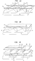
- FIG. 1A an isometric view of one preferred form of the invention is shown.
- the structure shown is formed on substrate 10 which could also comprise an upper layer of an integrated circuit device at an intermediate stage of formation.
- Contact studs 12 are shown for making contact with other conductors on or in substrate or layer 10.
- Extending between these contact studs 12 is a network of walls 14 formed of an insulating material which may form cells having an open or closed geometry in the plane of substrate or layer 10.
- the cell structure of Figure 1 a includes a pattern of closed polygons extending in a direction parallel to the substrate surface. These cells may be open in a direction perpendicular to the substrate surface.
- a fully closed cell structure is shown in the embodiment shown in Figure 1B.
- Conductor 16 is shown as extending across the tops of the contact studs and supported at intervals thereby, preferably on the order of 50 microns or less.
- Conductor 18 is shown as extending across the upper edges of insulating walls 14 and also supported thereby at intervals on the order of 50 microns or less.
- a combination of such supporting structures would normally be used in a particular device since a particular conductor would connect only a selected plurality of contact studs 12 while being supported at other locations by the upper edges of walls 14.
- the locations of conductors is relatively arbitrary as long as desired connections are made in accordance with the electrical design of the device.
- the formation of these conductors is referred to as "personalization” and the structure of a "device layer” (which could include a number of physical layers) for providing an interconnection pattern is often referred to as a "personalization layer”.
- the spacing of supports for a conductor in order to avoid conductor sagging which would cause shorting to another conductor in the same or an adjacent layer or sufficient elongation of a portion of the conductor to cause breakage or significant reduction in cross- sectional area of a conductor, is affected by both the layer thickness (e.g. the wall height) and the minimum feature size permitted under the design rules for a layer and neighboring layers.
- Increases in wall height tends to reduce capacitance between conductors but, for a given wall thickness, tends to reduce strength of the wall in regard to tolerance of shear forces.
- Increases in wall thickness tends to increase capacitance between conductors by increasing the average dielectric constant of the material interposed between the conductors.
- wall height is generally a small multiple (e.g. 2 to 5) of the wall width which cannot be less than the minimum feature size specified by the design rules.
- Walls 14 are preferably integrated with studs 12 in order to reinforce the latter.
- connections such as 16 and 18 must be formed on a planarized surface such as 20 of Figure 1B.
- Planarization of the surface requires some degree of mechanical polishing which, in turn, requires application of shear forces to the structure.
- Contact studs 12, alone are not capable of supporting such a surface during polishing and also will not generally be available to support conductors at the necessary intervals for all desired conductor locations.
- Walls 14 are therefore preferably located so that wall segments intersect at stud locations, as shown. Such location is not critical to the practice of the invention but results in maximum strength for with-standing polishing and other processing steps which can cause stress on the studs.
- cells formed by the pattern of wall segments 14 in accordance with the invention can be either closed polygons or open patterns which omit some wall segments or portions thereof.
- the cells of air dielectric structures in accordance with the invention can also be either open or closed from layer to layer depending on the presence or absence of layer 20 or openings therein. Even a relatively open pattern of wall segments 14 can form a closed polygon of relatively large size covering one or more regions of the wall pattern. when such a closed region is formed in a layer and the region is also to be closed by a surface 20, removal of removable material to form the air dielectric structure must be done before proceeding with the formation of subsequent device layers.
- the invention also provides for the formation of structures which may be open in directions either parallel or perpendicular to the plane of the substrate, or a combination of both.
- either open or closed cell structures may be employed which allow differing manufacturing sequences that may each be advantageous in particular manufacturing processes.
- Closed cell structures provide maximum lateral reinforcement of the studs 12 but require additional processing steps to remove material from the air dielectric cavities as each layer is formed.
- Open cell wall patterns such as that of Figure 15, have the advantage of allowing material removal from air dielectric volumes of a plurality of layers at the same time if openings are provided in layer 20. Further, since less material is provided in the walls 14 and layers 20 of open cell structures, a lower dielectric constant per unit length of conductor can be achieved.
- the practice of the invention is not limited to only one of open and closed cell structures in any device or even in any single layer within a device.
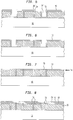
- a relatively thick layer (to define wall height) of removable material 30 has been deposited on a substrate 10 (which is assumed to include a conductive pattern (not shown)), which is, in turn, capped by a passivation layer 32 such as silicon dioxide deposited by a low temperature chemical vapor deposition (CVD) process or a composite passivation layer structure consisting of a layer of silicon dioxide, a reactive ion etch (RIE) stop layer of a material such as aluminum oxide, and a further top layer of silicon dioxide.
- the removable material 30 is preferably a water soluble glass or an organic polymer such as polyimide.
- the passivation layer is then masked for patterning with mask 34 which can be formed by any of many known processes such as photolithography or electron beam or x-ray lithography. It should be noted that mask 34 provides for the conductor pattern of the layer, depicted as narrow mask openings 38, and also for the desired pattern of conductive studs, depicted by wide mask openings 36.
- the passivation layer is then patterned using one or more etching steps appropriate to the composition thereof and the mask 34 removed, leaving the patterned passivation layer as a mask for removal of portions of the removable material layer 30. The removable material is then removed by dissolution or etching, leaving the structure shown in Figure 3.
- the wall segments form a two- dimensional network or pattern and that the intersection of walls occur at stud locations at as many locations as possible for structural robustness.
- the network of walls can be in any pattern such as triangles, squares, hexagons, etc. or portions thereof or serpentine patterns or portions thereof or combinations of any or all of these geometries.
- serpentine or hexagonal "honeycomb" patterns are preferred since they provide high strength with small wall thickness and also will usually provide a pattern which does not regularly extend directly between adjacent stud locations (e.g. from stud to stud).
- the rationale for this choice is that walls extending directly between stud locations, such as is shown at 42 and 44, increase the average dielectric constant and capacitive coupling between the studs.
- only the air dielectric is present at 46 and the capacitive coupling between studs 48 will be far less than between studs 48' even though the respective separations are similar and the studs connected structurally by two wall segments.
- wall network need not support all studs such as 48", since the structural robustness of the remainder of the wall network or pattern will effectively protect such areas from damage by shear forces during planarization polishing.
- a conformal layer of insulating material such as silicon dioxide is deposited, preferably by chemical vapor deposition.
- This conformal deposition does not have a preferred direction and forms sidewalls 52 in the stud openings 36' and fills wall openings 38' to form wall segments 54.
- etching in a preferentially vertical direction is done, preferably as a directional timed RIE etch back with a fluorinated hydrocarbon such and tetrafluoromethane, to remove the deposited insulator material from the upper surface of layer 32 and from the bottoms of the stud trenches 36'.
- Passivation layer 32 is of the same material (e.g. silicon dioxide) as the deposited material being etched and removal of some of the passivation layer 32 is largely irrelevant to the resulting structure if the passivation layer is initially formed with sufficient thickness.
- the stud trenches 36' are then filled, as shown at 70, with metal or other conductive material by any desired method and the surface planarized, removing deposited material from the surface by mechanical or chemical/mechanical polishing.
- the chemical composition of a polishing slurry can be adjusted to provide preferential material removal.
- it is desirable to provide for less removal of the deposited stud material so that the conductive material (e.g. metal) of studs 70 will slightly protrude from the surface or at least not be recessed below the surface of the layer. Since the removable material remains in place, the studs are not mechanically damaged by shear forces during planarization polishing.
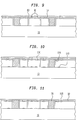
- insulator may be done to assure suitable remaining thickness 80, as shown in Figure 8, of passivation layer 32 to form a surface 20 of Figure 1B, if desired.
- Such an insulating and support layer would provide additional support for the conductors 16 since the residual passivation layer 32 may vary in thickness due to prior planarization processing such as chemical- mechanical polishing.
- one or more layers 80 are then deposited on planarized surface 72 of Figure 7. These layers may include further insulating material similar to the deposition during the planarization process described above and/or metal or other conductive material to form the next conductive pattern. This deposited material is then covered with mask layer 82 including apertures 84, preferably in the form of long, narrow slits in order to promote the rapid progress of removal of the removable material 30. Then, by RIE etching of the dielectric layers 80, 32, preferably in tetrafluoromethane, the slits 100 are formed through layers 80 and 32 to reach the removable material 30 which is then removed to form the air dielectric cavities, as shown in Figure 9.
- the slits are then closed by applying an insulative material such as silicon dioxide, preferably by a non-conformal CVD process.
- an insulative material such as silicon dioxide
- a non-conformal CVD process is highly directional, some deposition of material within the cavities is unavoidable as is shown at 110 and 114. However, this material does not significantly increase the average dielectric constant between conductors as long as the process is conducted in a manner to substantially maximize the directionality of the deposition.
- this closure of the slits may be omitted if planarization has been continued to level 74 ( Figure 6) and layer 80 is comprised only of conductor material. If this is the case, slits 84 can be wider and form the separation between conductors 16 and 18 of Figure 1A. However, no further layers could be applied above this layer.
- layer 80 does not contain conductors, it is necessary to again planarize the surface to expose studs 40 and deposit a conductive patternable layer 116 to complete the structure as shown in Figures 1B and 11. Filled layer 32 thus forms surface layer 20 of Figure 1B and conductor 16 of Figure 1B is formed by the patterning of layer 116.
- Figures 1B and 11 includes air dielectric cells which are potentially closed both by the closed polygons of the wall pattern and at the top and bottom by layers 20 or the substrate. Therefore it is necessary to remove the removable material 30 from closed cells as each layer is formed.
- only some portions of the wall pattern may include such closed cells and removal of the removable material from areas which contain only open wall patterns may be deferred for a plurality of layers. Since the removable material is preferably removable by plasma etching rather than wet etching, the material removal process can take place over a considerable thickness (e.g. number of layers) and tortuous paths without damage to the remainder of the structure. Nevertheless, the topology of the entire device design should be considered in the fabrication process to ensure that access to volumes of removable material will always be available in those areas where long conductor lines are present for connecting different functional blocks within the same chip.
- air dielectric structures can be limited to those areas which would benefit most from the electronic performance gain of an air dielectric scheme, such as long wiring lines between functional blocks on the same chip.
- metal stud and wiring areas of high density the formation of an air dielectric by the removal of a temporary dielectric can be difficult because of tight lithographic design rules.
- chip areas with a dielectric material are mechanically more stable than areas with an air dielectric. Therefore, it is desirable for the enhancement of structural reliability to limit the areas with an air dielectric.
- a compromise must be reached between areas with an air dielectric and areas with remaining removable dielectric material, as is preferred for ease of manufacturing.
- the choice of the removable dielectric material for a confined air dielectric concept should be a material with a low dielectric constant and with thermal stability in the temperature range commonly applied for wire interconnection schemes. Glasses like borosilicates of polymeric compounds such as polyimide are suitable for this purpose.
- the dielectric constant of air is, by definition, 1.0 and the dielectric constant of any applicable insulator is several times larger, the presence of insulator material in any location tends to increase capacitive coupling between conductors. Accordingly, the invention is intended to provide for a minimum of wall material to remain, consonant with maintaining sufficient structural robustness of the wall network or pattern. It should also be understood that the reduction of capacitive coupling between conductors addressed by this invention is a three-dimensional problem. All conductive structures, including studs 12, 70, which run in the same direction over any significant distance should be considered and the wall pattern adjusted to reduce capacitive coupling therebetween.
- the conductors associated with the substrate 10, assumed above, should be formed on the surface of the substrate rather than embedded in it, as shown in Figure 15. Likewise, conductors formed on subsequent layers 20 should not be embedded in the surface since the dielectric of the layer will serve to increase the capacitive coupling between conductors.
- the wall pattern or network should generally run at a large angle to the conductors either above or below. This is usually inherent in designs of multi-layer devices since conductors in alternate layers will generally run perpendicular to each other to maximize possibilities for interconnection by studs. However, this implies that conductors in a single layer will be run predominantly in parallel. In such a case, capacitive coupling can be minimized by placing walls on the conductors rather than between them whenever possible. In determining the possibility of so doing, walls should clearly not be positioned on conductors where conductors run in parallel in adjacent layers for the same reason that walls should not be run between adjacent studs as discussed above in connection with Figure 4.
- Figure 12 basically corresponds to the point of the above-described process illustrated in Figure 3.
- the illustrated structure is the same except that the thickness of substrate 10 is not depicted and surface 120 is intended to be generic to the surface of substrate 10 and the surface of any layer 20.
- the conductors 124 assumed and not illustrated in the foregoing discussion are now illustrated and covered by a further passivation layer 122. Trenches for walls and studs have been formed in the manner described above. It should also be noted that, if desired for larger stud cross-section, the stud trenches may be made significantly larger than the transverse dimension of the conductors 124, as shown by dashed lines 126.
- the sidewalls 132 which also serve to reinforce the studs against damage from shear forces can then reach to surface 120 and the stud, itself, can thus be formed with the same or larger transverse dimension than the conductor 124, as shown in Figure 13.
- FIG 13 which corresponds to the state of the above-described process depicted at Figure 6, the wall trenches have been filled and the stud sidewalls formed by conformal CVD.
- the etching to remove the passivation layer 122 over conductor 124 also opens layer 122 over conductor 124' in the wall trench 128.
- this latter opening is unimportant since the opening is then filled with insulating material which is unaffected, as before, by a subsequent etch back process to open the bottom of the stud trench to the conductor 124.
- the wall segment formed on conductor 124' is of a height which is reduced by the height of the conductor.
- a wall of such reduced height will be inherently more stable against shear forces than a full height wall.
- This stability may be enhanced greatly with little additional wall material by slightly increasing the thickness of such wall portions.
- This increase in stability can be exploited by reducing the wall thicknesses at other locations such as at 134 where, presumably, a wall was required at a position which was not matched by a conductor.
- the average dielectric constant between conductors 124' and 124'' can be held to a minimum even when the provision of a wall at such a location cannot be otherwise avoided in the wall network or pattern design.
- the device is completed by cell closure after removal of removable material as shown in Figure 14, which correspond to Figure 10 or 11 in the above described process.
- FIG. 15 in addition to forming walls on conductors, also differs from the embodiments of Figures 1A and 1B since the wall pattern is open in plan rather than being predominantly of closed polygons. Nevertheless, the embodiment of Figure 15 is potentially closed from layer to layer by layers 20. Openings could be left, however, to allow removal of removable material over several layers, as desired or dictated by the device design topology. Such a fully open design topology will now be described with reference to Figures 16 - 19.
- Figure 16 is a plan view of an open wall pattern such as might be employed in the embodiment of Figure 15.
- the walls 14 are preferably of a serpentine or other two- dimensional pattern to provide strength in shear in any direction. Additional short wall segments 160 can be included where desired or necessary.
- Figure 17 shows the structure after planarization, corresponding to the fabrication state shown in Figure 7 or 13 in the above described processes.
- passivation layer 32 is then removed, preferably by etching, and a conductive layer 180 directly applied to the resulting surface of studs 132, walls 134, 136 and removable material 30.
- Conductive layer may be a single layer of conductive material or a composite of a plurality of layers of differing materials, such as copper and gold to simultaneously achieve both high conductivity and strength.
- Conductive layer 180 may be applied in a desired pattern or patterned after application by known techniques as indicated at 182.
- a further layer of removable material 184 and passivation layer 184 may then be applied directly over the open conductor pattern and the process repeated as many times as desired, forming walls 160' and studs 132' as desired. It should be noted that any removable material which is attacked (e.g. at 190) during the patterning of conductive layer 180 will be replaced when the next layer of removable material is applied. It should be further noted that this process will allow formation of wall networks of closed polygon design, such as that of Figure 1A in multiple layers and without intervening insulative layer 20 of Figure 1B. Further, the number of steps of removing removable material is potentially reduced to one.
- the invention provides for the formation of a wide variety of air dielectric structures which are able to accommodate a wide variety of device designs as to both structural robustness and reduction of capacitive coupling between extended conductors. Further, it is to be understood that, within limits, structural robustness in one area of a device layer may be exploited in a neighboring area where reduction of capacitive coupling may be more critical. Air dielectric structures in accordance with the invention can be limited to those areas where the impact on electrical performance is most significant. By confining the air dielectric structures, the overall structural robustness of the chip is enhanced while signal coupling between long connection lines is minimized.
Landscapes
- Internal Circuitry In Semiconductor Integrated Circuit Devices (AREA)
- Semiconductor Integrated Circuits (AREA)
Applications Claiming Priority (2)
| Application Number | Priority Date | Filing Date | Title |
|---|---|---|---|
| US99067892A | 1992-12-15 | 1992-12-15 | |
| US990678 | 1997-12-15 |
Publications (1)
| Publication Number | Publication Date |
|---|---|
| EP0603104A1 true EP0603104A1 (fr) | 1994-06-22 |
Family
ID=25536415
Family Applications (1)
| Application Number | Title | Priority Date | Filing Date |
|---|---|---|---|
| EP93480194A Withdrawn EP0603104A1 (fr) | 1992-12-15 | 1993-11-19 | Procédé de personalisation d'un CI à grande échelle utilisant une structure diélectrique à l'air pour des conducteurs étendus |
Country Status (3)
| Country | Link |
|---|---|
| US (2) | US5530290A (fr) |
| EP (1) | EP0603104A1 (fr) |
| JP (1) | JPH0722583A (fr) |
Cited By (9)
| Publication number | Priority date | Publication date | Assignee | Title |
|---|---|---|---|---|
| DE4441898C1 (de) * | 1994-11-24 | 1996-04-04 | Siemens Ag | Verfahren zur Herstellung eines Halbleiterbauelementes |
| GB2306776A (en) * | 1995-10-17 | 1997-05-07 | Nec Corp | Multilevel interconnection structure |
| GB2327535A (en) * | 1997-07-18 | 1999-01-27 | Nec Corp | Interlevel dielectric |
| EP0924760A2 (fr) * | 1997-12-19 | 1999-06-23 | Texas Instruments Incorporated | Circuit de détection de transitions sur adresses |
| DE102005008476A1 (de) * | 2005-02-24 | 2006-09-14 | Infineon Technologies Ag | Leitbahnanordnung sowie zugehörige Herstellungsverfahren |
| EP1739737A1 (fr) * | 2005-06-13 | 2007-01-03 | Infineon Technologies AG | Méthode de formation d'une structure diélectrique à l'air |
| EP1668692A4 (fr) * | 2003-09-30 | 2007-05-09 | Ibm | Dielectrique reglable a entrefer auto-aligne pour cablage de faible capacite |
| WO2010022970A1 (fr) * | 2008-08-29 | 2010-03-04 | Advanced Micro Devices, Inc. | Dispositif à semi-conducteurs comprenant des espaces de relaxation de contrainte pour optimiser la stabilité d’interaction de boîtier de puce |
| CN102132406A (zh) * | 2008-08-29 | 2011-07-20 | 先进微装置公司 | 包含应力松弛间隙以提升芯片封装交互作用的稳定性的半导体设备 |
Families Citing this family (56)
| Publication number | Priority date | Publication date | Assignee | Title |
|---|---|---|---|---|
| US5516720A (en) * | 1994-02-14 | 1996-05-14 | United Microelectronics Corporation | Stress relaxation in dielectric before metallization |
| US5645684A (en) * | 1994-03-07 | 1997-07-08 | The Regents Of The University Of California | Multilayer high vertical aspect ratio thin film structures |
| US5750415A (en) * | 1994-05-27 | 1998-05-12 | Texas Instruments Incorporated | Low dielectric constant layers via immiscible sol-gel processing |
| KR0134108B1 (ko) * | 1994-06-30 | 1998-04-20 | 김주용 | 반도체 소자의 제조방법 |
| US5670828A (en) * | 1995-02-21 | 1997-09-23 | Advanced Micro Devices, Inc. | Tunneling technology for reducing intra-conductive layer capacitance |
| JP3359780B2 (ja) * | 1995-04-12 | 2002-12-24 | 三菱電機株式会社 | 配線装置 |
| US5981384A (en) * | 1995-08-14 | 1999-11-09 | Micron Technology, Inc. | Method of intermetal dielectric planarization by metal features layout modification |
| US5908318A (en) * | 1995-12-08 | 1999-06-01 | Advanced Micro Devices, Inc. | Method of forming low capacitance interconnect structures on semiconductor substrates |
| US5677241A (en) * | 1995-12-27 | 1997-10-14 | Micron Technology, Inc. | Integrated circuitry having a pair of adjacent conductive lines and method of forming |
| JP3887035B2 (ja) * | 1995-12-28 | 2007-02-28 | 株式会社東芝 | 半導体装置の製造方法 |
| US5869880A (en) * | 1995-12-29 | 1999-02-09 | International Business Machines Corporation | Structure and fabrication method for stackable, air-gap-containing low epsilon dielectric layers |
| JP2773729B2 (ja) * | 1996-02-29 | 1998-07-09 | 日本電気株式会社 | 半導体装置の製造方法 |
| US6057224A (en) * | 1996-03-29 | 2000-05-02 | Vlsi Technology, Inc. | Methods for making semiconductor devices having air dielectric interconnect structures |
| US5949144A (en) * | 1996-05-20 | 1999-09-07 | Harris Corporation | Pre-bond cavity air bridge |
| US5814555A (en) | 1996-06-05 | 1998-09-29 | Advanced Micro Devices, Inc. | Interlevel dielectric with air gaps to lessen capacitive coupling |
| US5953626A (en) * | 1996-06-05 | 1999-09-14 | Advanced Micro Devices, Inc. | Dissolvable dielectric method |
| US6376330B1 (en) | 1996-06-05 | 2002-04-23 | Advanced Micro Devices, Inc. | Dielectric having an air gap formed between closely spaced interconnect lines |
| US6429120B1 (en) | 2000-01-18 | 2002-08-06 | Micron Technology, Inc. | Methods and apparatus for making integrated-circuit wiring from copper, silver, gold, and other metals |
| US6746959B2 (en) * | 1996-07-26 | 2004-06-08 | Lg Philips Lcd Co., Ltd. | Liquid crystal display and method |
| US5731223A (en) * | 1996-09-24 | 1998-03-24 | Lsi Logic Corporation | Array of solder pads on an integrated circuit |
| US5744865A (en) * | 1996-10-22 | 1998-04-28 | Texas Instruments Incorporated | Highly thermally conductive interconnect structure for intergrated circuits |
| US6037253A (en) * | 1997-01-27 | 2000-03-14 | Chartered Semiconductor Manufacturing Company, Ltd. | Method for increasing interconnect packing density in integrated circuits |
| US6333255B1 (en) | 1997-08-21 | 2001-12-25 | Matsushita Electronics Corporation | Method for making semiconductor device containing low carbon film for interconnect structures |
| US5891797A (en) * | 1997-10-20 | 1999-04-06 | Micron Technology, Inc. | Method of forming a support structure for air bridge wiring of an integrated circuit |
| US5869379A (en) * | 1997-12-08 | 1999-02-09 | Advanced Micro Devices, Inc. | Method of forming air gap spacer for high performance MOSFETS' |
| US6160316A (en) * | 1998-03-04 | 2000-12-12 | Advanced Micro Devices, Inc. | Integrated circuit utilizing an air gap to reduce capacitance between adjacent metal linewidths |
| US7211496B1 (en) * | 1998-04-22 | 2007-05-01 | International Business Machines Corporation | Freestanding multiplayer IC wiring structure |
| US6097092A (en) | 1998-04-22 | 2000-08-01 | International Business Machines Corporation | Freestanding multilayer IC wiring structure |
| US6509590B1 (en) * | 1998-07-20 | 2003-01-21 | Micron Technology, Inc. | Aluminum-beryllium alloys for air bridges |
| US6268261B1 (en) * | 1998-11-03 | 2001-07-31 | International Business Machines Corporation | Microprocessor having air as a dielectric and encapsulated lines and process for manufacture |
| US6071805A (en) * | 1999-01-25 | 2000-06-06 | Chartered Semiconductor Manufacturing, Ltd. | Air gap formation for high speed IC processing |
| JP2000332010A (ja) * | 1999-03-17 | 2000-11-30 | Canon Sales Co Inc | 層間絶縁膜の形成方法及び半導体装置 |
| US6130151A (en) * | 1999-05-07 | 2000-10-10 | Taiwan Semiconductor Manufacturing Company | Method of manufacturing air gap in multilevel interconnection |
| US6204165B1 (en) | 1999-06-24 | 2001-03-20 | International Business Machines Corporation | Practical air dielectric interconnections by post-processing standard CMOS wafers |
| US6556962B1 (en) | 1999-07-02 | 2003-04-29 | Intel Corporation | Method for reducing network costs and its application to domino circuits |
| US6255712B1 (en) | 1999-08-14 | 2001-07-03 | International Business Machines Corporation | Semi-sacrificial diamond for air dielectric formation |
| US6211057B1 (en) * | 1999-09-03 | 2001-04-03 | Taiwan Semiconductor Manufacturing Company | Method for manufacturing arch air gap in multilevel interconnection |
| TW439147B (en) * | 1999-12-20 | 2001-06-07 | United Microelectronics Corp | Manufacturing method to form air gap using hardmask to improve isolation effect |
| FR2803092B1 (fr) * | 1999-12-24 | 2002-11-29 | St Microelectronics Sa | Procede de realisation d'interconnexions metalliques isolees dans des circuits integres |
| US6420262B1 (en) | 2000-01-18 | 2002-07-16 | Micron Technology, Inc. | Structures and methods to enhance copper metallization |
| US7262130B1 (en) | 2000-01-18 | 2007-08-28 | Micron Technology, Inc. | Methods for making integrated-circuit wiring from copper, silver, gold, and other metals |
| US7211512B1 (en) | 2000-01-18 | 2007-05-01 | Micron Technology, Inc. | Selective electroless-plated copper metallization |
| US6674167B1 (en) | 2000-05-31 | 2004-01-06 | Micron Technology, Inc. | Multilevel copper interconnect with double passivation |
| US6423629B1 (en) | 2000-05-31 | 2002-07-23 | Kie Y. Ahn | Multilevel copper interconnects with low-k dielectrics and air gaps |
| JP2002231721A (ja) * | 2001-02-06 | 2002-08-16 | Mitsubishi Electric Corp | 半導体装置 |
| DE10161312A1 (de) * | 2001-12-13 | 2003-07-10 | Infineon Technologies Ag | Verfahren zum Herstellen einer Schicht-Anordnung und Schicht-Anordnung |
| US20040077107A1 (en) * | 2002-10-17 | 2004-04-22 | Nantero, Inc. | Method of making nanoscopic tunnel |
| US20040087162A1 (en) * | 2002-10-17 | 2004-05-06 | Nantero, Inc. | Metal sacrificial layer |
| US6713835B1 (en) * | 2003-05-22 | 2004-03-30 | International Business Machines Corporation | Method for manufacturing a multi-level interconnect structure |
| US20080029841A1 (en) * | 2003-11-03 | 2008-02-07 | International Business Machines Corporation | Structure and method for forming a dielectric chamber and electronic device including dielectric chamber |
| US7018916B2 (en) * | 2003-11-03 | 2006-03-28 | International Business Machines Corporation | Structure and method for forming a dielectric chamber and electronic device including the dielectric chamber |
| US7094689B2 (en) * | 2004-07-20 | 2006-08-22 | Taiwan Semiconductor Manufacturing Co., Ltd. | Air gap interconnect structure and method thereof |
| US7439172B2 (en) * | 2007-01-16 | 2008-10-21 | International Business Machines Corporation | Circuit structure with low dielectric constant regions and method of forming same |
| US7485567B2 (en) * | 2007-02-02 | 2009-02-03 | International Business Machines Corporation | Microelectronic circuit structure with layered low dielectric constant regions and method of forming same |
| US7896692B2 (en) * | 2009-05-15 | 2011-03-01 | Leviton Manufacturing Co., Inc. | Method of improving isolation between circuits on a printed circuit board |
| DE102020202262A1 (de) * | 2020-02-21 | 2021-08-26 | Robert Bosch Gesellschaft mit beschränkter Haftung | Verfahren zur Herstellung einer nanoskaligen Kanalstruktur |
Citations (3)
| Publication number | Priority date | Publication date | Assignee | Title |
|---|---|---|---|---|
| US3890636A (en) * | 1971-09-09 | 1975-06-17 | Hitachi Ltd | Multilayer wiring structure of integrated circuit and method of producing the same |
| EP0476625A2 (fr) * | 1990-09-18 | 1992-03-25 | Nec Corporation | Dispositif semi-conducteur comprenant des interconnexions |
| EP0550910A1 (fr) * | 1991-12-31 | 1993-07-14 | Texas Instruments Incorporated | Technique d'interconnection multi-niveaux à basse valeur RC pour circuits intégrés à haute performance |
Family Cites Families (10)
| Publication number | Priority date | Publication date | Assignee | Title |
|---|---|---|---|---|
| US3925880A (en) * | 1971-04-29 | 1975-12-16 | Signetics Corp | Semiconductor assembly with beam lead construction and method |
| JPS63179548A (ja) * | 1987-01-21 | 1988-07-23 | Mitsubishi Electric Corp | 半導体集積回路装置の配線構造 |
| JPH0783053B2 (ja) * | 1987-06-19 | 1995-09-06 | 三菱電機株式会社 | 半導体装置 |
| JPS6489939A (en) * | 1987-09-28 | 1989-04-05 | Tokai Rubber Ind Ltd | Brush for small-sized motor |
| JPH01189939A (ja) * | 1988-01-26 | 1989-07-31 | Nec Corp | 半導体集積回路 |
| JPH01318248A (ja) * | 1988-06-20 | 1989-12-22 | Fujitsu Ltd | 半導体装置及びその製造方法 |
| JPH0727968B2 (ja) * | 1988-12-20 | 1995-03-29 | 株式会社東芝 | 半導体集積回路装置 |
| JPH02220464A (ja) * | 1989-02-22 | 1990-09-03 | Toshiba Corp | 半導体装置及びその製造方法 |
| US4933743A (en) * | 1989-03-11 | 1990-06-12 | Fairchild Semiconductor Corporation | High performance interconnect system for an integrated circuit |
| US5372969A (en) * | 1991-12-31 | 1994-12-13 | Texas Instruments Incorporated | Low-RC multi-level interconnect technology for high-performance integrated circuits |
-
1993
- 1993-09-06 JP JP5220798A patent/JPH0722583A/ja active Pending
- 1993-11-19 EP EP93480194A patent/EP0603104A1/fr not_active Withdrawn
-
1994
- 1994-04-11 US US08/226,103 patent/US5530290A/en not_active Expired - Fee Related
- 1994-04-11 US US08/225,685 patent/US5444015A/en not_active Expired - Fee Related
Patent Citations (3)
| Publication number | Priority date | Publication date | Assignee | Title |
|---|---|---|---|---|
| US3890636A (en) * | 1971-09-09 | 1975-06-17 | Hitachi Ltd | Multilayer wiring structure of integrated circuit and method of producing the same |
| EP0476625A2 (fr) * | 1990-09-18 | 1992-03-25 | Nec Corporation | Dispositif semi-conducteur comprenant des interconnexions |
| EP0550910A1 (fr) * | 1991-12-31 | 1993-07-14 | Texas Instruments Incorporated | Technique d'interconnection multi-niveaux à basse valeur RC pour circuits intégrés à haute performance |
Non-Patent Citations (2)
| Title |
|---|
| "Method to improve dielectric properties of insulators", IBM TECHNICAL DISCLOSURE BULLETIN., vol. 32, no. 5B, October 1989 (1989-10-01), NEW YORK US, pages 418 - 419 * |
| "Structure and Method for Making Multilevel Air Bridge Wiring", IBM TECHNICAL DISCLOSURE BULLETIN., vol. 32, no. 8A, January 1990 (1990-01-01), NEW YORK US, pages 88 - 89 * |
Cited By (21)
| Publication number | Priority date | Publication date | Assignee | Title |
|---|---|---|---|---|
| EP0714129A2 (fr) | 1994-11-24 | 1996-05-29 | Siemens Aktiengesellschaft | Dispositif semi-conducteur |
| US5882963A (en) * | 1994-11-24 | 1999-03-16 | Siemens Aktiengesellschaft | Method of manufacturing semiconductor components |
| DE4441898C1 (de) * | 1994-11-24 | 1996-04-04 | Siemens Ag | Verfahren zur Herstellung eines Halbleiterbauelementes |
| GB2306776A (en) * | 1995-10-17 | 1997-05-07 | Nec Corp | Multilevel interconnection structure |
| US6051491A (en) * | 1995-10-17 | 2000-04-18 | Nec Corporation | Multilevel interconnection structure for integrated circuits and method of producing same |
| GB2306776B (en) * | 1995-10-17 | 2000-08-23 | Nec Corp | Multilevel interconnection structure |
| CN1061785C (zh) * | 1995-10-17 | 2001-02-07 | 日本电气株式会社 | 用于集成电路的多层互连及其制造方法 |
| GB2327535A (en) * | 1997-07-18 | 1999-01-27 | Nec Corp | Interlevel dielectric |
| GB2327535B (en) * | 1997-07-18 | 1999-09-15 | Nec Corp | Semiconductor device and method of forming semiconductor device |
| EP0924760A2 (fr) * | 1997-12-19 | 1999-06-23 | Texas Instruments Incorporated | Circuit de détection de transitions sur adresses |
| EP1668692A4 (fr) * | 2003-09-30 | 2007-05-09 | Ibm | Dielectrique reglable a entrefer auto-aligne pour cablage de faible capacite |
| DE102005008476A1 (de) * | 2005-02-24 | 2006-09-14 | Infineon Technologies Ag | Leitbahnanordnung sowie zugehörige Herstellungsverfahren |
| DE102005008476B4 (de) * | 2005-02-24 | 2006-12-21 | Infineon Technologies Ag | Leitbahnanordnung sowie zugehöriges Herstellungsverfahren |
| US8877631B2 (en) | 2005-02-24 | 2014-11-04 | Infineon Technologies Ag | Interconnect arrangement and associated production methods |
| EP1739737A1 (fr) * | 2005-06-13 | 2007-01-03 | Infineon Technologies AG | Méthode de formation d'une structure diélectrique à l'air |
| US7629225B2 (en) | 2005-06-13 | 2009-12-08 | Infineon Technologies Ag | Methods of manufacturing semiconductor devices and structures thereof |
| US8013364B2 (en) | 2005-06-13 | 2011-09-06 | Infineon Technologies Ag | Semiconductor devices and structures thereof |
| US8148235B2 (en) | 2005-06-13 | 2012-04-03 | Infineon Technologies Ag | Methods of manufacturing semiconductor devices |
| US9401322B2 (en) | 2005-06-13 | 2016-07-26 | Infineon Technologies Ag | Semiconductor devices and structures thereof |
| WO2010022970A1 (fr) * | 2008-08-29 | 2010-03-04 | Advanced Micro Devices, Inc. | Dispositif à semi-conducteurs comprenant des espaces de relaxation de contrainte pour optimiser la stabilité d’interaction de boîtier de puce |
| CN102132406A (zh) * | 2008-08-29 | 2011-07-20 | 先进微装置公司 | 包含应力松弛间隙以提升芯片封装交互作用的稳定性的半导体设备 |
Also Published As
| Publication number | Publication date |
|---|---|
| JPH0722583A (ja) | 1995-01-24 |
| US5444015A (en) | 1995-08-22 |
| US5530290A (en) | 1996-06-25 |
Similar Documents
| Publication | Publication Date | Title |
|---|---|---|
| US5530290A (en) | Large scale IC personalization method employing air dielectric structure for extended conductor | |
| EP2264758B1 (fr) | Structure d'interconnexion dans un dispositif semiconducteur | |
| JP2587857B2 (ja) | 埋込み多重レベル間相互接続体装置 | |
| US6830970B2 (en) | Inductance and via forming in a monolithic circuit | |
| US4996133A (en) | Self-aligned tungsten-filled via process and via formed thereby | |
| JP2001515654A (ja) | 集積回路用配線方式 | |
| US6097092A (en) | Freestanding multilayer IC wiring structure | |
| US6576525B2 (en) | Damascene capacitor having a recessed plate | |
| US6110824A (en) | Wire shape conferring reduced crosstalk and formation methods | |
| US8679937B2 (en) | Method for fabricating a capacitor and capacitor structure thereof | |
| CN111066146A (zh) | 三维存储器件中的具有处于衬底内的导电部分的接触结构及其形成方法 | |
| US9837305B1 (en) | Forming deep airgaps without flop over | |
| EP1743366B1 (fr) | Structure de cablage pour circuit integre a capacite intercouche reduite | |
| US7211496B1 (en) | Freestanding multiplayer IC wiring structure | |
| US7109565B2 (en) | Finger metal-insulator-metal capacitor device with local interconnect | |
| EP0924762A2 (fr) | Interconnexions pour circuits intégrés | |
| KR100310470B1 (ko) | 양면반도체메모리소자및그제조방법 | |
| US6706589B2 (en) | Manufacturing of capacitors with metal armatures | |
| US6413855B2 (en) | Methods of making interconnections for semiconductor circuits | |
| US10186491B2 (en) | Integrated circuit chip reinforced against front side deprocessing attacks | |
| JPH0581180B2 (fr) | ||
| US5212352A (en) | Self-aligned tungsten-filled via | |
| TWI699874B (zh) | 半導體結構及其製造方法 | |
| KR100252884B1 (ko) | 반도체 소자의 배선 형성방법 | |
| CN121941339A (zh) | 半导体器件及其制造方法、电子设备 |
Legal Events
| Date | Code | Title | Description |
|---|---|---|---|
| PUAI | Public reference made under article 153(3) epc to a published international application that has entered the european phase |
Free format text: ORIGINAL CODE: 0009012 |
|
| AK | Designated contracting states |
Kind code of ref document: A1 Designated state(s): DE FR GB |
|
| 17P | Request for examination filed |
Effective date: 19941021 |
|
| 17Q | First examination report despatched |
Effective date: 19970618 |
|
| STAA | Information on the status of an ep patent application or granted ep patent |
Free format text: STATUS: THE APPLICATION IS DEEMED TO BE WITHDRAWN |
|
| 18D | Application deemed to be withdrawn |
Effective date: 19971230 |