EP0603585A1 - Elément optique, méthode de fabrication d'une couche, couche ou structure à couches et leur utilisation - Google Patents
Elément optique, méthode de fabrication d'une couche, couche ou structure à couches et leur utilisation Download PDFInfo
- Publication number
- EP0603585A1 EP0603585A1 EP93119085A EP93119085A EP0603585A1 EP 0603585 A1 EP0603585 A1 EP 0603585A1 EP 93119085 A EP93119085 A EP 93119085A EP 93119085 A EP93119085 A EP 93119085A EP 0603585 A1 EP0603585 A1 EP 0603585A1
- Authority
- EP
- European Patent Office
- Prior art keywords
- layer
- layers
- zro2
- wear protection
- component according
- Prior art date
- Legal status (The legal status is an assumption and is not a legal conclusion. Google has not performed a legal analysis and makes no representation as to the accuracy of the status listed.)
- Granted
Links
Images


Classifications
-
- G02B1/105—
-
- G—PHYSICS
- G02—OPTICS
- G02B—OPTICAL ELEMENTS, SYSTEMS OR APPARATUS
- G02B1/00—Optical elements characterised by the material of which they are made; Optical coatings for optical elements
- G02B1/10—Optical coatings produced by application to, or surface treatment of, optical elements
- G02B1/14—Protective coatings, e.g. hard coatings
Definitions
- the present invention relates to an optical component according to the preamble of claim 1, a method for producing a layer according to that of claim 11, a layer according to the wording of claim 15 and a use according to that of claim 20.
- Optical components for influencing the transmission of light in the visible spectrum have long been known, e.g. of coated glasses.
- the mode of operation of such an optical component is based on the principle of interference, and therefore at least one transition between a high-index and a low-index material is provided.
- Spectral range corresponding to a light wavelength from 380nm to 780nm.
- the individual layers are typically thinner than 100 nm.
- oxides of group IVa such as TiO2, ZrO2, HfO2, group IVb, here especially SiO2, group IIIa, such as Al2O3, Y2O3, Sc2O3, further group Va, such as Ta2O5, Nb2O3 , and oxides or fluorides of some rare earths, such as CeO2, LaF2, and fluorides of groups IIa and lead fluoride and silicon nitride are used.
- group IVa such as TiO2, ZrO2, HfO2, group IVb
- SiO2, group IIIa such as Al2O3, Y2O3, Sc2O3, further group Va, such as Ta2O5, Nb2O3
- oxides or fluorides of some rare earths such as CeO2, LaF2, and fluorides of groups IIa and lead fluoride and silicon nitride are used.
- the hardness of the layers of the materials mentioned, which are usually produced by vapor deposition, is relatively low, often less than the Knoop hardness HK 50g of machine glass , which is approx. 650.
- Wear-resistant hard coating systems must have a total thickness of ⁇ 100nm.
- wear protection layer systems of the specified minimum thickness consisting of the specified layer materials, with the exception of BN and diamond, have an average extinction constant, averaged in any spectral band, of at least 10 nm within the visible light spectrum, which is significantly greater than 5 ⁇ 10 ⁇ 2
- layer systems of the specified thickness have an average transmission, in the spectral band mentioned, which is significantly smaller than 10%
- BN and diamond layers are currently not usable for optical purposes in the visible spectral range and with commercially reasonable effort.
- the present invention has for its object to provide an optical component of the type mentioned, in which a high level of wear protection is guaranteed.
- the wear protection system is the totality of all layers consisting of the materials mentioned, the number of which is at least one layer, and in particular regardless of whether there are further layers between these layers to achieve a desired optical effect, but none of them or provide negligible wear protection.
- the substrate mentioned can be designed on both sides or on one side according to the invention, but the values given below with respect to average transmission also relate to a substrate coated on one side or to a single wear protection system.
- an average transmission is achieved on the optical component according to the invention even over a spectral band that is substantially wider than 10 nm, preferably is at least 100 nm or even extends over a substantial part of the visible light spectrum.
- a glass is preferably used as the substrate on the optical component, the hardness of at least one of the layers of the wear protection system being greater than that of the glass. This ensures that the glass is protected against wear by said at least one layer, specifically regardless of whether or not further layers are provided above this layer and / or between it and the glass surface. It is essential that the above-mentioned layer, like the wear protection system provided according to the invention at all, only insignificantly worsens or even improves a desired optical effect, for example an additionally provided layer system.
- ZrO2 and (Al, Cr) 2O3 are to be designated as preferred layer materials today in the wear protection system provided according to the invention.
- the wear protection effect of the system is significantly increased and nevertheless not impossible to achieve the desired optical properties realize.
- a preferred embodiment of the wear protection system according to the wording of claim 5 has at least one layer of ZrO2 with a hardness of at least 1000 Vickers, preferably even at least 1200 Vickers.
- the wear protection system provided according to the invention has at least one layer made of the material, which is produced by ion plating. All of the layers mentioned are preferably produced from the materials mentioned by ion plating.
- the compressive stress in the layer should preferably be within the range specified in claim 7.
- the advantage of producing the above-mentioned layers by means of ion plating is, in particular, that relatively low temperatures can be maintained with this method, for example from below 900 ° C. down to approximately 450 ° C. and less, and this is particularly true for the production of (Al, Cr) 2O3 layers, whereupon the alpha phase is stabilized by adding Cr.
- the optical component can be constructed in a preferred manner according to the wording of claim 8.
- a component according to the invention in addition to the abrasion protection system mentioned, can have further layers — temporarily stored in the abrasion protection system, above or below it, so that the abrasion protection system becomes part of an overall layer system on the substrate.
- a metal layer or a metallic layer can additionally be provided, such as a silver, gold, titanium nitride or hafnium nitride layer. These layers are used to achieve the desired transmission or reflection behavior, not for the purpose of protecting against wear.
- the inventive method particularly preferably for the production of a layer of ZrO2 or (Al, Cr) 2O3 is characterized by the wording of claim 11 and, as has been explained, consists in producing such a layer by ion plating.
- a layer according to the invention is particularly characterized by ZrO2 or (Al, Cr) 2O3 according to the wording of claim 15, in that it only enables the use mentioned that the layer-specific, average extinction constant is at most 5 ⁇ 10 ⁇ 2.
- Such a layer or such a layer system is preferably deposited on glass, plastic or a metal or semiconductor as a carrier substrate and in particular, deposited on glass, for watch glasses, bar code scanner or welding protection devices.
- curve shape 'a' denotes the behavior of an optical component according to Example 1, but without a first layer
- curve shape 'b' represents the optical behavior of the component according to the invention with the first layer ensuring wear protection
- the reflection behavior of this component according to the invention is shown in FIG. 2.
- the reflection at 633nm is 0.065%.
- the reflection at 633nm is 4.2%.
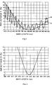
- the reflection behavior of the optical component according to example 3 is shown in FIG. 3, the course 'a' representing the course on the same component, but without a first layer, that is to say without a wear protection layer, while course 'b' representing the reflection course on the component provided with a wear protection layer according to the invention.
- the absorption A ( ⁇ ), defined by the percentage of light I o absorbed by the incident light I A is shown over the essential spectral range of the visible light, for a 1 micron and a 2 micron thick (Al, Cr) 203 layer .
- the 2 ⁇ m layer absorbs a maximum of approx. 30%, the 1 ⁇ m layer a maximum of approx. 16%.
- the k ( ⁇ ) values are significantly smaller than 5 ⁇ 10 ⁇ 2, indeed considerably smaller than 10 ⁇ 2 in the entire spectral range under consideration.
- both the (Al, Cr) 2O3 layer and the ZrO2 layer were deposited with the system subsequently described, as is shown schematically in FIG. 5.
- It is a BAP800 type ion plating system known per se, as manufactured by the applicant. It comprises a vacuum recipient 1 with a workpiece carrier cap 3, which is mounted on the wall 5 of the recipient 1 in an electrically insulated, rotationally driven manner. It carries workpieces 7.
- an ionization chamber 9 is flanged, which communicates with the interior of the recipient 1 via an aperture 11, both electrically insulated with respect to the wall 5 and also with respect to the wall of the ionization chamber 9.
- An electron emission cathode 13 in the form of a hot cathode is provided in the ionization chamber 9, connected to a heating current generator 15.
- a working gas preferably argon
- a working gas is admitted into the ionization chamber 9 via a connection 17 via a control valve 19.
- One or, as shown, two or more selectively connectable electron beam evaporation devices 21a and 21b form the respectively activated anodes of the low-voltage discharge path. As shown schematically with the switch S, they can be placed selectively with respect to the hot cathode 13 at anodic potential via source 23.
- a reactive gas outlet arrangement 27 is provided in the recipient 1, connected in the case mentioned here, via a control valve arrangement 29, to an oxygen tank 31.
- 3 radiant heaters 33 are provided in the area of the rotary cap.
- the wear protection layer (Al, CR) 2O3 according to Examples 1 to 3 was produced as follows:
- the sizes HK further denote the Knoop hardness and HV the Vickers hardness.
- the (Al, Cr) 2O3 layers produced as described in the examples given have a refractive index between 1.8 and 1.9 at a wavelength of 550 nm and an extinction constant k (550 nm) ⁇ 5 ⁇ 10 at this wavelength ⁇ 3.
- the optical components according to the invention can also be used in particular for applications in which glass, such as clear glass, green glass, quartz glass etc., metals or semiconductors are to be protected against wear, i.e. the optical component according to the invention and / or in particular the one according to the invention optically transparent wear protection layer typically used for watch glass coatings, bar code scanner covers, applications in the context of welding protection devices, etc., therefore in principle for applications in which such elements are exposed to severe wear and tear, for example, in industrial production and in correspondingly harsh environmental conditions, and which should still maintain their optical behavior.
- glass such as clear glass, green glass, quartz glass etc.
- metals or semiconductors are to be protected against wear
Landscapes
- Physics & Mathematics (AREA)
- General Physics & Mathematics (AREA)
- Optics & Photonics (AREA)
- Surface Treatment Of Glass (AREA)
- Physical Vapour Deposition (AREA)
- Laminated Bodies (AREA)
- Surface Treatment Of Optical Elements (AREA)
Applications Claiming Priority (3)
| Application Number | Priority Date | Filing Date | Title |
|---|---|---|---|
| CH3901/92 | 1992-12-21 | ||
| CH390192 | 1992-12-21 | ||
| CH390192 | 1992-12-21 |
Publications (2)
| Publication Number | Publication Date |
|---|---|
| EP0603585A1 true EP0603585A1 (fr) | 1994-06-29 |
| EP0603585B1 EP0603585B1 (fr) | 2000-02-09 |
Family
ID=4265940
Family Applications (1)
| Application Number | Title | Priority Date | Filing Date |
|---|---|---|---|
| EP93119085A Expired - Lifetime EP0603585B1 (fr) | 1992-12-21 | 1993-11-26 | Elément optique, méthode de fabrication d'une couche, couche ou structure à couches et utilisation de l'élément optique |
Country Status (4)
| Country | Link |
|---|---|
| US (1) | US5537257A (fr) |
| EP (1) | EP0603585B1 (fr) |
| JP (1) | JPH06265701A (fr) |
| DE (1) | DE59309954D1 (fr) |
Families Citing this family (2)
| Publication number | Priority date | Publication date | Assignee | Title |
|---|---|---|---|---|
| US6012830A (en) * | 1998-06-23 | 2000-01-11 | Valeo Sylvania L.L.C. | Light shield for a vehicle headlamp |
| WO2010001804A1 (fr) | 2008-07-01 | 2010-01-07 | 住友電気工業株式会社 | Procédé de production d'un monocristal d'alxga(1-x)n, monocristal d'alxga(1‑x)n et optiques |
Citations (4)
| Publication number | Priority date | Publication date | Assignee | Title |
|---|---|---|---|---|
| DD120190A1 (fr) * | 1975-04-02 | 1976-06-05 | ||
| JPS62270074A (ja) * | 1986-05-19 | 1987-11-24 | Fuji Photo Film Co Ltd | 消去可能な静止画像録画装置 |
| JPH02225033A (ja) * | 1989-02-28 | 1990-09-07 | Nippon Steel Corp | 耐食性に優れたセラミック被覆材 |
| GB2252333A (en) * | 1991-01-29 | 1992-08-05 | Spectra Physics Scanning Syst | Scanner window coated with hard material and then with lubricous coating |
Family Cites Families (16)
| Publication number | Priority date | Publication date | Assignee | Title |
|---|---|---|---|---|
| US3934961A (en) * | 1970-10-29 | 1976-01-27 | Canon Kabushiki Kaisha | Three layer anti-reflection film |
| US3958042A (en) * | 1971-04-05 | 1976-05-18 | Agency Of Industrial Science & Technology | Method for manufacture of reflection-proof film |
| US4129434A (en) * | 1971-07-08 | 1978-12-12 | Glaverbell | Process for forming a metal oxide coating |
| US3815978A (en) * | 1972-06-20 | 1974-06-11 | Ibm | Durable see-through photoresist mask |
| DE2658418A1 (de) * | 1976-12-23 | 1978-06-29 | Leybold Heraeus Gmbh & Co Kg | Verfahren zur herstellung von antireflexschichten auf acrylglaesern, nach dem verfahren hergestellter optischer koerper und verwendung des optischen koerpers |
| JPS5727263A (en) * | 1980-07-28 | 1982-02-13 | Hitachi Ltd | Electrophotographic photosensitive film |
| JPS62270774A (ja) * | 1986-05-16 | 1987-11-25 | Sumitomo Electric Ind Ltd | 硬質透光膜で被覆した装飾品 |
| US4822466A (en) * | 1987-06-25 | 1989-04-18 | University Of Houston - University Park | Chemically bonded diamond films and method for producing same |
| US5216551A (en) * | 1990-02-16 | 1993-06-01 | Asahi Kogaku Kogyo K.K. | Surface reflector |
| JPH0413251A (ja) * | 1990-04-28 | 1992-01-17 | Kyocera Corp | 光磁気記録素子及びその製造方法 |
| US5168023A (en) * | 1990-07-04 | 1992-12-01 | Matsushita Electric Industrial Co., Ltd. | Photosensitive element used in electrophotography |
| US5310607A (en) * | 1991-05-16 | 1994-05-10 | Balzers Aktiengesellschaft | Hard coating; a workpiece coated by such hard coating and a method of coating such workpiece by such hard coating |
| US5286217A (en) * | 1991-08-15 | 1994-02-15 | Foxconn International | Electrical connector with improved latch mechanism |
| GB2261079B (en) * | 1991-10-31 | 1995-06-14 | Asahi Optical Co Ltd | Surface reflecting mirror |
| JPH05286249A (ja) * | 1992-02-10 | 1993-11-02 | Hitachi Ltd | 情報記録用媒体 |
| US5346600A (en) * | 1992-08-14 | 1994-09-13 | Hughes Aircraft Company | Plasma-enhanced magnetron-sputtered deposition of materials |
-
1993
- 1993-11-26 DE DE59309954T patent/DE59309954D1/de not_active Expired - Fee Related
- 1993-11-26 EP EP93119085A patent/EP0603585B1/fr not_active Expired - Lifetime
- 1993-12-15 US US08/167,767 patent/US5537257A/en not_active Expired - Fee Related
- 1993-12-21 JP JP5321765A patent/JPH06265701A/ja active Pending
Patent Citations (4)
| Publication number | Priority date | Publication date | Assignee | Title |
|---|---|---|---|---|
| DD120190A1 (fr) * | 1975-04-02 | 1976-06-05 | ||
| JPS62270074A (ja) * | 1986-05-19 | 1987-11-24 | Fuji Photo Film Co Ltd | 消去可能な静止画像録画装置 |
| JPH02225033A (ja) * | 1989-02-28 | 1990-09-07 | Nippon Steel Corp | 耐食性に優れたセラミック被覆材 |
| GB2252333A (en) * | 1991-01-29 | 1992-08-05 | Spectra Physics Scanning Syst | Scanner window coated with hard material and then with lubricous coating |
Non-Patent Citations (2)
| Title |
|---|
| PATENT ABSTRACTS OF JAPAN vol. 12, no. 154 (C - 495) 14 May 1988 (1988-05-14) * |
| PATENT ABSTRACTS OF JAPAN vol. 14, no. 532 (M - 1051) 22 November 1990 (1990-11-22) * |
Also Published As
| Publication number | Publication date |
|---|---|
| JPH06265701A (ja) | 1994-09-22 |
| US5537257A (en) | 1996-07-16 |
| EP0603585B1 (fr) | 2000-02-09 |
| DE59309954D1 (de) | 2000-03-16 |
Similar Documents
| Publication | Publication Date | Title |
|---|---|---|
| DE102004062289B4 (de) | Thermisch stabiler Multilayer-Spiegel für den EUV-Spektralbereich | |
| EP0632850B1 (fr) | Corps composite et son utilisation | |
| EP0564709B1 (fr) | Substrat transparent revêtu, son emploi, procédé de fabrication des revêtements et dispositif pour la mise en oeuvre d'un tel procédé et oxynitrure d'hafnium | |
| EP3158370B1 (fr) | Élément optique muni d'un revêtement réfléchissant | |
| DE69115363T2 (de) | Infrarotdurchlässiges Schutzfenster | |
| EP0685297A1 (fr) | Outil pour des appareils de formage et de coupage et procédé de fabrication un outil revêtu | |
| EP0620456A1 (fr) | Miroir à argent à haute réflexion | |
| DE102015103494B4 (de) | Verfahren zur Herstellung eines Reflektorelements und Reflektorelement | |
| DE4112114C1 (fr) | ||
| CH658522A5 (de) | Optisches element. | |
| DE19537263C2 (de) | Transparente Wärmeschutzfolie und Verfahren zu deren Herstellung | |
| DE4324325B4 (de) | Verfahren zur Herstellung eines Bauelementes, optisches Bauelement, Verwendung desselben und Vakuumbehandlungsanlage zu seiner Herstellung | |
| DE10126364B9 (de) | Aluminium-Reflexionsspiegel und Verfahren zu dessen Herstellung | |
| DE3720451A1 (de) | Schlagfeste und gehaertete optische elemente | |
| EP0603585B1 (fr) | Elément optique, méthode de fabrication d'une couche, couche ou structure à couches et utilisation de l'élément optique | |
| DE102020000305A1 (de) | Beschichtetes Schneidwerkzeug | |
| EP3779526A1 (fr) | Procédé de fabrication d'une couche d'aluminium et élément optique | |
| DE102006006283A1 (de) | Thermisch stabiler Multilayer-Spiegel für den EUV-Spektralbereich | |
| DE69025860T2 (de) | Optische Elemente und Methode zu deren Erzeugung | |
| DE2720742A1 (de) | Mehrschicht-antireflexbelag fuer glassubstrate | |
| DE3786245T2 (de) | Verfahren zur Herstellung eines magnetischen dünnen Polstücks. | |
| DE102006011973B4 (de) | Spiegel mit einer Silberschicht | |
| DE102013108315A1 (de) | Beschichtungsvorrichtung und Verfahren zum Herstellen einer Beschichtungsvorrichtung | |
| DE19838826B4 (de) | Optisches Element mit transparenter, kratzfester Beschichtung, Verfahren und Vorrichtung zu seiner Herstellung sowie dessen Verwendung | |
| DE112008001939B4 (de) | Oxidfilm, Oxidfilm-beschichtetes Material und Verfahren zum Bilden eines Oxidfilms |
Legal Events
| Date | Code | Title | Description |
|---|---|---|---|
| PUAI | Public reference made under article 153(3) epc to a published international application that has entered the european phase |
Free format text: ORIGINAL CODE: 0009012 |
|
| AK | Designated contracting states |
Kind code of ref document: A1 Designated state(s): BE CH DE FR GB IT LI |
|
| K1C3 | Correction of patent application (complete document) published |
Effective date: 19940629 |
|
| RIN1 | Information on inventor provided before grant (corrected) |
Inventor name: RUDIGIER, HELMUT, DR. DIPL.-PHYS. ETH |
|
| 17P | Request for examination filed |
Effective date: 19941205 |
|
| 17Q | First examination report despatched |
Effective date: 19961010 |
|
| GRAG | Despatch of communication of intention to grant |
Free format text: ORIGINAL CODE: EPIDOS AGRA |
|
| GRAG | Despatch of communication of intention to grant |
Free format text: ORIGINAL CODE: EPIDOS AGRA |
|
| GRAH | Despatch of communication of intention to grant a patent |
Free format text: ORIGINAL CODE: EPIDOS IGRA |
|
| GRAH | Despatch of communication of intention to grant a patent |
Free format text: ORIGINAL CODE: EPIDOS IGRA |
|
| GRAA | (expected) grant |
Free format text: ORIGINAL CODE: 0009210 |
|
| AK | Designated contracting states |
Kind code of ref document: B1 Designated state(s): BE CH DE FR GB IT LI |
|
| PG25 | Lapsed in a contracting state [announced via postgrant information from national office to epo] |
Ref country code: IT Free format text: LAPSE BECAUSE OF FAILURE TO SUBMIT A TRANSLATION OF THE DESCRIPTION OR TO PAY THE FEE WITHIN THE PRE;WARNING: LAPSES OF ITALIAN PATENTS WITH EFFECTIVE DATE BEFORE 2007 MAY HAVE OCCURRED AT ANY TIME BEFORE 2007. THE CORRECT EFFECTIVE DATE MAY BE DIFFERENT FROM THE ONE RECORDED.SCRIBED TIME-LIMIT Effective date: 20000209 |
|
| REG | Reference to a national code |
Ref country code: CH Ref legal event code: EP |
|
| GBT | Gb: translation of ep patent filed (gb section 77(6)(a)/1977) |
Effective date: 20000209 |
|
| REF | Corresponds to: |
Ref document number: 59309954 Country of ref document: DE Date of ref document: 20000316 |
|
| ET | Fr: translation filed | ||
| GBT | Gb: translation of ep patent filed (gb section 77(6)(a)/1977) |
Free format text: ERRATUM: THE FOLLOWING EUROPEAN PATENTS WERE ADVERTISED IN ERROR IN JOURNAL 5781 DATED 1 MARCH 2000 AS HAVING BEEN FILED UNDER SECTION 77(6)(A) ON 8 FEBRUARY 2000. |
|
| PG25 | Lapsed in a contracting state [announced via postgrant information from national office to epo] |
Ref country code: BE Free format text: LAPSE BECAUSE OF NON-PAYMENT OF DUE FEES Effective date: 20001130 |
|
| PLBE | No opposition filed within time limit |
Free format text: ORIGINAL CODE: 0009261 |
|
| STAA | Information on the status of an ep patent application or granted ep patent |
Free format text: STATUS: NO OPPOSITION FILED WITHIN TIME LIMIT |
|
| 26N | No opposition filed | ||
| BERE | Be: lapsed |
Owner name: BALZERS A.G. Effective date: 20001130 |
|
| REG | Reference to a national code |
Ref country code: GB Ref legal event code: IF02 |
|
| PGFP | Annual fee paid to national office [announced via postgrant information from national office to epo] |
Ref country code: FR Payment date: 20021108 Year of fee payment: 10 |
|
| PGFP | Annual fee paid to national office [announced via postgrant information from national office to epo] |
Ref country code: GB Payment date: 20021120 Year of fee payment: 10 |
|
| PGFP | Annual fee paid to national office [announced via postgrant information from national office to epo] |
Ref country code: CH Payment date: 20030214 Year of fee payment: 10 |
|
| PG25 | Lapsed in a contracting state [announced via postgrant information from national office to epo] |
Ref country code: GB Free format text: LAPSE BECAUSE OF NON-PAYMENT OF DUE FEES Effective date: 20031126 |
|
| PG25 | Lapsed in a contracting state [announced via postgrant information from national office to epo] |
Ref country code: LI Free format text: LAPSE BECAUSE OF NON-PAYMENT OF DUE FEES Effective date: 20031130 Ref country code: CH Free format text: LAPSE BECAUSE OF NON-PAYMENT OF DUE FEES Effective date: 20031130 |
|
| GBPC | Gb: european patent ceased through non-payment of renewal fee |
Effective date: 20031126 |
|
| REG | Reference to a national code |
Ref country code: CH Ref legal event code: PL |
|
| PG25 | Lapsed in a contracting state [announced via postgrant information from national office to epo] |
Ref country code: FR Free format text: LAPSE BECAUSE OF NON-PAYMENT OF DUE FEES Effective date: 20040730 |
|
| REG | Reference to a national code |
Ref country code: FR Ref legal event code: ST |
|
| PGFP | Annual fee paid to national office [announced via postgrant information from national office to epo] |
Ref country code: DE Payment date: 20051124 Year of fee payment: 13 |
|
| PG25 | Lapsed in a contracting state [announced via postgrant information from national office to epo] |
Ref country code: DE Free format text: LAPSE BECAUSE OF NON-PAYMENT OF DUE FEES Effective date: 20070601 |