EP0604893B1 - Appareil à cristal liquide - Google Patents
Appareil à cristal liquide Download PDFInfo
- Publication number
- EP0604893B1 EP0604893B1 EP93120666A EP93120666A EP0604893B1 EP 0604893 B1 EP0604893 B1 EP 0604893B1 EP 93120666 A EP93120666 A EP 93120666A EP 93120666 A EP93120666 A EP 93120666A EP 0604893 B1 EP0604893 B1 EP 0604893B1
- Authority
- EP
- European Patent Office
- Prior art keywords
- display device
- substrate
- drive circuit
- film carrier
- unit
- Prior art date
- Legal status (The legal status is an assumption and is not a legal conclusion. Google has not performed a legal analysis and makes no representation as to the accuracy of the status listed.)
- Expired - Lifetime
Links
Images




Classifications
-
- H—ELECTRICITY
- H05—ELECTRIC TECHNIQUES NOT OTHERWISE PROVIDED FOR
- H05K—PRINTED CIRCUITS; CASINGS OR CONSTRUCTIONAL DETAILS OF ELECTRIC APPARATUS; MANUFACTURE OF ASSEMBLAGES OF ELECTRICAL COMPONENTS
- H05K3/00—Apparatus or processes for manufacturing printed circuits
- H05K3/0058—Laminating printed circuit boards onto other substrates, e.g. metallic substrates
-
- G—PHYSICS
- G02—OPTICS
- G02F—OPTICAL DEVICES OR ARRANGEMENTS FOR THE CONTROL OF LIGHT BY MODIFICATION OF THE OPTICAL PROPERTIES OF THE MEDIA OF THE ELEMENTS INVOLVED THEREIN; NON-LINEAR OPTICS; FREQUENCY-CHANGING OF LIGHT; OPTICAL LOGIC ELEMENTS; OPTICAL ANALOGUE/DIGITAL CONVERTERS
- G02F1/00—Devices or arrangements for the control of the intensity, colour, phase, polarisation or direction of light arriving from an independent light source, e.g. switching, gating or modulating; Non-linear optics
- G02F1/01—Devices or arrangements for the control of the intensity, colour, phase, polarisation or direction of light arriving from an independent light source, e.g. switching, gating or modulating; Non-linear optics for the control of the intensity, phase, polarisation or colour
- G02F1/13—Devices or arrangements for the control of the intensity, colour, phase, polarisation or direction of light arriving from an independent light source, e.g. switching, gating or modulating; Non-linear optics for the control of the intensity, phase, polarisation or colour based on liquid crystals, e.g. single liquid crystal display cells
- G02F1/133—Constructional arrangements; Operation of liquid crystal cells; Circuit arrangements
- G02F1/1333—Constructional arrangements; Manufacturing methods
- G02F1/1345—Conductors connecting electrodes to cell terminals
- G02F1/13452—Conductors connecting driver circuitry and terminals of panels
-
- H—ELECTRICITY
- H05—ELECTRIC TECHNIQUES NOT OTHERWISE PROVIDED FOR
- H05K—PRINTED CIRCUITS; CASINGS OR CONSTRUCTIONAL DETAILS OF ELECTRIC APPARATUS; MANUFACTURE OF ASSEMBLAGES OF ELECTRICAL COMPONENTS
- H05K1/00—Printed circuits
- H05K1/02—Details
- H05K1/0277—Bendability or stretchability details
- H05K1/028—Bending or folding regions of flexible printed circuits
-
- H—ELECTRICITY
- H05—ELECTRIC TECHNIQUES NOT OTHERWISE PROVIDED FOR
- H05K—PRINTED CIRCUITS; CASINGS OR CONSTRUCTIONAL DETAILS OF ELECTRIC APPARATUS; MANUFACTURE OF ASSEMBLAGES OF ELECTRICAL COMPONENTS
- H05K1/00—Printed circuits
- H05K1/02—Details
-
- H—ELECTRICITY
- H05—ELECTRIC TECHNIQUES NOT OTHERWISE PROVIDED FOR
- H05K—PRINTED CIRCUITS; CASINGS OR CONSTRUCTIONAL DETAILS OF ELECTRIC APPARATUS; MANUFACTURE OF ASSEMBLAGES OF ELECTRICAL COMPONENTS
- H05K2201/00—Indexing scheme relating to printed circuits covered by H05K1/00
- H05K2201/01—Dielectrics
- H05K2201/0104—Properties and characteristics in general
- H05K2201/0133—Elastomeric or compliant polymer
-
- H—ELECTRICITY
- H05—ELECTRIC TECHNIQUES NOT OTHERWISE PROVIDED FOR
- H05K—PRINTED CIRCUITS; CASINGS OR CONSTRUCTIONAL DETAILS OF ELECTRIC APPARATUS; MANUFACTURE OF ASSEMBLAGES OF ELECTRICAL COMPONENTS
- H05K2201/00—Indexing scheme relating to printed circuits covered by H05K1/00
- H05K2201/03—Conductive materials
- H05K2201/0332—Structure of the conductor
- H05K2201/0388—Other aspects of conductors
- H05K2201/0394—Conductor crossing over a hole in the substrate or a gap between two separate substrate parts
-
- H—ELECTRICITY
- H05—ELECTRIC TECHNIQUES NOT OTHERWISE PROVIDED FOR
- H05K—PRINTED CIRCUITS; CASINGS OR CONSTRUCTIONAL DETAILS OF ELECTRIC APPARATUS; MANUFACTURE OF ASSEMBLAGES OF ELECTRICAL COMPONENTS
- H05K2201/00—Indexing scheme relating to printed circuits covered by H05K1/00
- H05K2201/09—Shape and layout
- H05K2201/09009—Substrate related
- H05K2201/09063—Holes or slots in insulating substrate not used for electrical connections
-
- H—ELECTRICITY
- H05—ELECTRIC TECHNIQUES NOT OTHERWISE PROVIDED FOR
- H05K—PRINTED CIRCUITS; CASINGS OR CONSTRUCTIONAL DETAILS OF ELECTRIC APPARATUS; MANUFACTURE OF ASSEMBLAGES OF ELECTRICAL COMPONENTS
- H05K2201/00—Indexing scheme relating to printed circuits covered by H05K1/00
- H05K2201/09—Shape and layout
- H05K2201/09209—Shape and layout details of conductors
- H05K2201/09218—Conductive traces
- H05K2201/09281—Layout details of a single conductor
-
- H—ELECTRICITY
- H05—ELECTRIC TECHNIQUES NOT OTHERWISE PROVIDED FOR
- H05K—PRINTED CIRCUITS; CASINGS OR CONSTRUCTIONAL DETAILS OF ELECTRIC APPARATUS; MANUFACTURE OF ASSEMBLAGES OF ELECTRICAL COMPONENTS
- H05K2201/00—Indexing scheme relating to printed circuits covered by H05K1/00
- H05K2201/10—Details of components or other objects attached to or integrated in a printed circuit board
- H05K2201/10007—Types of components
- H05K2201/10128—Display
- H05K2201/10136—Liquid Crystal display [LCD]
-
- H—ELECTRICITY
- H05—ELECTRIC TECHNIQUES NOT OTHERWISE PROVIDED FOR
- H05K—PRINTED CIRCUITS; CASINGS OR CONSTRUCTIONAL DETAILS OF ELECTRIC APPARATUS; MANUFACTURE OF ASSEMBLAGES OF ELECTRICAL COMPONENTS
- H05K2201/00—Indexing scheme relating to printed circuits covered by H05K1/00
- H05K2201/10—Details of components or other objects attached to or integrated in a printed circuit board
- H05K2201/10227—Other objects, e.g. metallic pieces
- H05K2201/10409—Screws
-
- H—ELECTRICITY
- H05—ELECTRIC TECHNIQUES NOT OTHERWISE PROVIDED FOR
- H05K—PRINTED CIRCUITS; CASINGS OR CONSTRUCTIONAL DETAILS OF ELECTRIC APPARATUS; MANUFACTURE OF ASSEMBLAGES OF ELECTRICAL COMPONENTS
- H05K2201/00—Indexing scheme relating to printed circuits covered by H05K1/00
- H05K2201/10—Details of components or other objects attached to or integrated in a printed circuit board
- H05K2201/10431—Details of mounted components
- H05K2201/10598—Means for fastening a component, a casing or a heat sink whereby a pressure is exerted on the component towards the PCB
-
- H—ELECTRICITY
- H05—ELECTRIC TECHNIQUES NOT OTHERWISE PROVIDED FOR
- H05K—PRINTED CIRCUITS; CASINGS OR CONSTRUCTIONAL DETAILS OF ELECTRIC APPARATUS; MANUFACTURE OF ASSEMBLAGES OF ELECTRICAL COMPONENTS
- H05K2201/00—Indexing scheme relating to printed circuits covered by H05K1/00
- H05K2201/10—Details of components or other objects attached to or integrated in a printed circuit board
- H05K2201/10613—Details of electrical connections of non-printed components, e.g. special leads
- H05K2201/10621—Components characterised by their electrical contacts
- H05K2201/10681—Tape Carrier Package [TCP]; Flexible sheet connector
-
- H—ELECTRICITY
- H05—ELECTRIC TECHNIQUES NOT OTHERWISE PROVIDED FOR
- H05K—PRINTED CIRCUITS; CASINGS OR CONSTRUCTIONAL DETAILS OF ELECTRIC APPARATUS; MANUFACTURE OF ASSEMBLAGES OF ELECTRICAL COMPONENTS
- H05K3/00—Apparatus or processes for manufacturing printed circuits
- H05K3/36—Assembling printed circuits with other printed circuits
- H05K3/361—Assembling flexible printed circuits with other printed circuits
Definitions
- the present invention relates to a liquid crystal apparatus according the preamble of claim 1.
- a liquid crystal apparatus is known on which the preamble of claim 1 is based.
- a carrier consisting of an insulating substrate and of a conductor establishes an electric contact between a display device and a drive circuit unit.
- the insulating substrate is partially removed from the conductor to provide an opening where the carrier is folded or bent.
- the display device is folded perpendicular to the drive circuit unit. Due to this, a unit substrate carrying the drive circuit unit is perpendicular to the display device.
- a display device has been driven by, e.g., an external drive circuit unit as schematically illustrated in Figure 8. More specifically, a drive circuit 802 and a bus substrate (unit substrate) 803 supplying electricity and signals to the drive circuit 802 constitute a module which is fixed to a chassis 904 as shown in Figure 9.
- the bus substrate 803 is electrically and mechanically connected with a flexible film carrier (flexible bus tape) 805 at an input-side outer lead part 807 and a display device 801 is electrically and mechanically connected with the film carrier 805 at an output-side outer lead part 806.
- the film carrier 805 is loaded with the drive circuit 802.
- the bus substrate (unit substrate) has been fixed to a panel (display device)-fixing member has been effected, for example, as illustrated in Figure 18.
- a panel 1201 is fixed to a panel-fixing member 1203 with an adhesive of, e.g., silicone rubber, and a bus substrate (unit substrate) 1202 is fixed to the panel-fixing member 1203 with screws 1209, etc.
- the panel 1201 generally comprises a pair of glass substrates 1801a and 1801b each provided with transparent electrodes (not shown) and a liquid crystal (not shown) sealed between the glass substrates, so as to apply drive voltages to the transparent electrodes for driving the liquid crystal.
- a drive IC 1205 for controlling drive signals mounted on a film carrier 1206 (TAB film) is electrically connected to the bus substrate 1202 and the panel 1201 via the lead 1207 of the film carrier by the outer-lead-bonding method.
- Behind the panel 1201 is disposed a backlight 1208 for illuminating the panel 1201.
- the bus substrate 1202 and a CPU substrate (not shown) for controlling the entire liquid crystal apparatus are electrically connected via a flat cable 1210.
- the bus substrate 1202 and the panel fixing member 1203 are integrally fixed, so that a stress is directly applied to the joint of the lead 1207 of the film carrier 1206, thus resulting in a difficulty, such as breakage of the lead of the film carrier 1206.
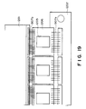
- Figure 19 is an enlarged view of the joints between the film carrier 1206 and the panel 1201 and the bus substrate 1202.
- the lead 1907 of the film carrier 1206 and the bus substrate are jointed at a pitch of ordinarily 0.3 - 1 mm
- the lead 1907b of the film carrier 1206 and the panel 1201 are jointed at a narrower pitch of about 0.1 - 0.3 mm.
- the leads 1907b of the film carrier 1208 become thin and are liable to be broken at a small force.
- the panel 1201 is ordinarily composed by glass and the panel-fixing member 1203 is frequently composed by a plastic material, so that there is a remarkable difference in thermal expansion coefficient therebetween.
- the panel fixing member 1203 may be elongated, whereas the panel 1201 having a remarkably smaller thermal expansion coefficient may not be substantially elongated.
- the panel fixing member 1203 moves in a direction of an arrow A , whereas the movement of the panel 1201 can be substantially negligible.
- the bus substrate 1202 is integrally fixed to the panel-fixing member 1203 with screws and is therefore moved along with the elongation of the panel-fixing member 1203.
- an object of the present invention is to provide a liquid crystal apparatus including a film carrier which is capable of facilitating the assembling of the apparatus and yet is tough against an external stress.
- a liquid crystal apparatus shall be provided including a film carrier capable of decreasing the stress applied to leads thereof even when a positional deviation is caused between the panel and the panel fixing member due to a difference in thermal expansion coefficient.
- a liquid crystal apparatus comprising: a display device for data display, a unit substrate for supplying electric signals, and a film carrier loaded with a drive IC for driving the display device and connecting the display device and the unit substrate, wherein said unit substrate has a fixing hole and is fastened to a supporting member with a screw having a head and a shank inserted through the fixing hole, and a space regulating means is disposed between the screw head and the unit substrate so as to leave a spacing between the screw shank and the unit substrate, thereby providing an allowance for movement of the unit substrate relative to the supporting member.
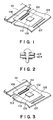
- Figure 1 is a perspective view showing a first embodiment of the joint structure used in the liquid crystal apparatus according to the invention.
- Figure 2 is a partial sectional view of a fixing structure of a bus substrate according to the first embodiment.
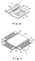
- Figures 3 - 6 are respectively a perspective view showing another embodiment of the joint structure according to the invention.
- Figure 7 is a perspective view showing a liquid crystal apparatus including a display device (panel), and drive circuits and bus substrates connected to the display device according to the first embodiment.
- Figure 8 is a perspective view showing a conventional joint structure among a display device, a drive circuit and a bus substrate.
- Figure 9 is a sectional view corresponding to Figure 8.
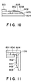
- Figure 10 is a perspective view showing another conventional joint structure among a display device, a drive circuit and a bus substrate.
- Figure 11 is a sectional view corresponding to Figure 10.
- Figure 12 is a perspective view showing a embodiment according to a second aspect of the liquid crystal apparatus according to the invention.
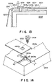
- Figure 13 is a partial sectional view corresponding to Figure 12.
- Figure 14 is a partial exploded view corresponding to Figure 12.
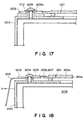
- Figures 15 - 17 are respectively a partial sectional view showing a joint structure according to another embodiment of the present invention.
- Figure 18 is a partial sectional view showing a conventional joint structure for a liquid crystal drive substrate.
- Figure 19 is a partial plan view corresponding to Figure 18.
- FIG. 1 is a partial sectional view of a first embodiment of the present invention showing a manner of assembling an external drive circuit with a display device.
- a tape-form film carrier 105 mounted with a drive circuit 102 is provided with a blank (film-removed part, referred to as a first blank) 111 at two parts between an inner lead 110 and an output-side outer lead 106 thereof.
- the blanks 111 are formed by punching at an early stage of preparation of the film carrier 105 similarly as a device hole for mounting the drive circuit 102 and input-side outer leads 107.
- it is also possible to form such blanks by etching of a film carrier formed from, e.g., a photosensitive polyimide.
- the output-side outer leads 106 of the film carrier 105 are electrically and mechanically connected to electrodes of a display device 101 via, e.g., an anisotropic conductor film.
- the input-side outer leads 107 are electrically and mechanically connected to a substrate, e.g., by soldering.
- the display device 101 is fixed to a chassis 204, e.g., by bonding, and the bus substrate 103 is half-fixed to the chassis in a manner as shown in Figure 2.
- the bus substrate 103 When such a module is supplied with an external impact or vibration, the bus substrate 103 is moved so that the film carrier 105 is supplied with a stress.
- the stress can be relaxed by the blanks 111 provided to the film of the film carrier 105 without forming a stepwise forming part 1008 as shown in Figure 10, which, if formed, is liable to cause an unnecessary deformation of the bus substrate 103 (corresponding to "803" in Figure 10). Accordingly, it is possible to obviate the damage of the drive circuit 2 and electric wires.
- a polyimide layer 312 in a thickness of ca. 30 - 40 ⁇ m at film blanks 311 so as to facilitate the handling without impairing the stress relaxation effect.
- a polyimide layer 312 in a thickness of ca. 30 - 40 ⁇ m at film blanks 311 so as to facilitate the handling without impairing the stress relaxation effect.
- the copper foils (conductors) 413 at the blanks 111 in the shape of lightning or snakes as shown in Figure 4, it is also possible to enhance the stress relaxation effect.
- FIG. 5 is a perspective view showing a joint structure used in a liquid crystal apparatus according to the present invention for assembling an external drive circuit with a display device.
- a film carrier 105 mounted with a drive circuit 102 is provided with blanks 512 (second blanks) of film substrate at two parts between an inner lead 110 and an input-side outer lead 107.
- This embodiment may show an effect of relaxing an external stress similarly as the first embodiment, so as to prevent the damage of the drive circuit 102 and electric wires.
- Figure 6 is a perspective view showing a third embodiment of assembling an external drive circuit with a display device.
- input-side inner leads 607 of a film carrier 105 mounted with a drive circuit 102 are disposed to extend in a direction perpendicular to a direction toward output-side outer leads 106 and the display device 101.
- the film carrier 105 and the bus substrate 103 are firmly connected to each other to suppress the movement of the bus substrate 103. This is particularly effective for a large-sized display device, such as one having a diagonal size in excess of 20 inches, requiring a large and heavy bus substrate.
- FIG. 7 is a perspective view showing a fourth embodiment of assembling an external drive circuit with a display device.
- fixing members 713 are disposed to bridge between a display device 101 and bus substrates 103, e.g., by bonding.
- the bus substrates 103 are fixed in a planar direction with respect to the display device 101.
- the bus substrates are not readily dislocated in X and Y directions in Figure 7 but are liable to be dislocated in a Q-direction (rotational direction).
- the film carriers 105 are allowed to retain a flexibility with respect to the dislocation in the Q direction, thereby preventing damages of the drive circuits 102 and electric wires.
- FIG 12 is a perspective view showing an embodiment of the liquid crystal apparatus according to the present invention
- Figure 13 is a sectional view showing a fixing structure where a display device is screwed to a panel fixing member.
- the fixing structure includes a display device 1201, a unit substrate 1202 for supplying electricity and signals, a panel-fixing member 1203, a silicone adhesive 1204 for bonding the panel 1202, a drive IC 1205 carried on a film carrier 1206 having a lead 1207, a backlight 1208, a screw 1209 and a flat cable 1210.
- a boss 1303a (boss part) having a diameter smaller than that of a hole provided to the unit substrate 1202 for fixing the unit substrate 1202 and a rib 1303b for receiving the unit substrate 1202. Further, the screw 1209 is tightened into the boss 1303a in the form of covering the hole for fixing the unit substrate with its head.
- Figure 14 is an exploded view of the fixing structure including the drive unit substrate 1202, the panel fixing substrate 1203 and the screw 1209 shown in Figure 13.
- the unit substrate 1202 is mounted on the ribs 1303b of the panel-fixing member 1203 with its lower surface and fixed by the screw 1209.
- a height h measured from the upper surface of the ribs 1303b to the upper surface of the boss 1303a is set to be slightly larger, e.g., by ca. 0.1 - 0.2 mm than the thickness t of the unit substrate 1202.
- the screw 1209 is stopped upon the upper surface of the boss 1303a and can regulate the vertical position of the unit substrate 1202 with a slight play without tightening the unit substrate 1202 per se because of the relationship of t ⁇ h.
- the diameter of the fixing hole 1402a bored in the unit substrate is denoted by D and the diameter of the boss 1303a is denoted by d , there is formed a gap of (D-d)/2 between the boss 1303a and the unit substrate 1202 surrounding the hole 1402a if the fixing hole 1402a and the boss 1303a are coaxially aligned.
- the gap is denoted by x
- the unit substrate 1202 is set movably by a distance x relative to the panel-fixing member 1203 in a planer direction parallel to the panel 1201.
- the unit substrate 1202 is not affected by the movement of the fixing member 1203 if the relative deviation y is within the range of x-y > 0, so that the breakage of the leads of the film carrier 1206 can be obviated.
- a liquid crystal apparatus including a display panel 1201 having a size of 300 mm and a fixing member 1203 having a size of 370 mm respectively along one side of the apparatus caused a lead breakage when subjected to an environmental temperature change of from 25 °C to 60 °C.
- the difference in elongation between the panel 1201 and the panel-fixing member 1203 at that time was about 0.6 mm. Accordingly, if the elongation occurs in equal degrees at both ends, the positional deviation y between the panel 1201 and the fixing member 1203 amounts to a half thereof, so that an adequate tolerance can be attained if x is set to satisfy x > 0.3 for the above-mentioned sizes and the temperature ranges.
- the ribs 1303b are selected as a contacting member between the unit substrate 1202 and the fixing member 1202 so as to facilitate the relative movement therebetween, but a roughly similar good result can be obtained even if the lower surface of the unit substrate 1202 and the upper surface 1303c of the panel-fixing member 1203 contact each other.
Landscapes
- Physics & Mathematics (AREA)
- Engineering & Computer Science (AREA)
- Microelectronics & Electronic Packaging (AREA)
- Nonlinear Science (AREA)
- Manufacturing & Machinery (AREA)
- Mathematical Physics (AREA)
- Chemical & Material Sciences (AREA)
- Crystallography & Structural Chemistry (AREA)
- General Physics & Mathematics (AREA)
- Optics & Photonics (AREA)
- Devices For Indicating Variable Information By Combining Individual Elements (AREA)
- Liquid Crystal (AREA)
Claims (6)
- Appareil à cristal liquide, comportant : un dispositif d'affichage (101) destiné à afficher des données, une unité à circuit d'attaque (102) destinée à attaquer le dispositif d'affichage, un substrat d'unité (103) destiné à fournir des signaux électriques à l'unité à circuit d'attaque, et un support (105) de film en forme de bande comportant un substrat isolant et un conducteur recouvert du substrat isolant pour connecter l'unité à circuit d'attaque au dispositif d'affichage et au substrat d'unité, dans lequel
une partie (106) du support de film (105) connectant le dispositif d'affichage (101) à l'unité à circuit d'attaque (102) et/ou l'unité à circuit d'attaque (102) au substrat d'unité (103) est pourvue d'au moins une partie vierge (111, 512) où le substrat isolant est enlevé localement pour mettre à nu le conducteur, caractérisé en ce que ledit substrat d'unité (103) et ledit dispositif d'affichage (101) sont juxtaposés dans une disposition sensiblement plane afin que ladite, au moins une, partie vierge absorbe efficacement une contrainte appliquée extérieurement au support (105) de film. - Appareil de cristal liquide selon la revendication 1, dans lequel ledit support (105) de film est connecté au substrat d'unité (103) par l'intermédiaire de conducteur de sortie (607) s'étendant dans une direction perpendiculaire à une direction orientée vers la partie (106) du support de film (105) connectant le dispositif d'affichage (101) et l'unité à circuit d'attaque (102).
- Appareil selon la revendication 1 ou 2, dans lequel ladite unité à circuit d'attaque (102) et ledit substrat d'unité (103) sont connectés avec ledit support de film (105) à une partie latérale du support de film (105) en forme de bande par rapport à une direction longitudinale dans laquelle le dispositif d'affichage et l'unité à circuit d'attaque sont connectés.
- Appareil selon la revendication 1 ou 2, dans lequel ladite partie vierge (111 ; 512) est revêtue d'un polyimide d'une épaisseur d'environ 30 à 40 µm.
- Appareil selon la revendication 1 ou 2, dans lequel ledit conducteur à nu à ladite partie vierge (111 ; 512) est formé dans la configuration d'un éclair ou en zig-zag afin d'accroítre l'absorption d'une contrainte extérieure.
- Appareil selon la revendication 1 ou 2, dans lequel il y a plusieurs parties vierges (111, 512).
Applications Claiming Priority (6)
| Application Number | Priority Date | Filing Date | Title |
|---|---|---|---|
| JP35931692A JPH06202137A (ja) | 1992-12-26 | 1992-12-26 | 液晶装置 |
| JP35931392A JPH06202136A (ja) | 1992-12-26 | 1992-12-26 | 液晶装置 |
| JP359316/92 | 1992-12-26 | ||
| JP35931392 | 1992-12-26 | ||
| JP359313/92 | 1992-12-26 | ||
| JP35931692 | 1992-12-26 |
Publications (3)
| Publication Number | Publication Date |
|---|---|
| EP0604893A2 EP0604893A2 (fr) | 1994-07-06 |
| EP0604893A3 EP0604893A3 (fr) | 1995-01-18 |
| EP0604893B1 true EP0604893B1 (fr) | 2002-05-02 |
Family
ID=26580948
Family Applications (1)
| Application Number | Title | Priority Date | Filing Date |
|---|---|---|---|
| EP93120666A Expired - Lifetime EP0604893B1 (fr) | 1992-12-26 | 1993-12-22 | Appareil à cristal liquide |
Country Status (3)
| Country | Link |
|---|---|
| US (2) | US5517208A (fr) |
| EP (1) | EP0604893B1 (fr) |
| DE (1) | DE69331873T2 (fr) |
Cited By (1)
| Publication number | Priority date | Publication date | Assignee | Title |
|---|---|---|---|---|
| CN111836460A (zh) * | 2020-07-21 | 2020-10-27 | 方炜 | 一种线路板及其制备方法 |
Families Citing this family (34)
| Publication number | Priority date | Publication date | Assignee | Title |
|---|---|---|---|---|
| US5808707A (en) * | 1995-03-01 | 1998-09-15 | Canon Kabushiki Kaisha | Display apparatus |
| US5936850A (en) * | 1995-03-03 | 1999-08-10 | Canon Kabushiki Kaisha | Circuit board connection structure and method, and liquid crystal device including the connection structure |
| JP3098392B2 (ja) * | 1995-03-03 | 2000-10-16 | シャープ株式会社 | 実装基板及びそれを用いた液晶モジュール |
| JP3139601B2 (ja) * | 1995-03-08 | 2001-03-05 | キヤノン株式会社 | 液晶表示装置 |
| US6683594B1 (en) * | 1995-04-20 | 2004-01-27 | Canon Kabushiki Kaisha | Display apparatus and assembly of its driving circuit |
| JPH08314390A (ja) * | 1995-05-16 | 1996-11-29 | Nec Shizuoka Ltd | 個別呼出用受信機のリフレクタ保持構造 |
| US6281891B1 (en) | 1995-06-02 | 2001-08-28 | Xerox Corporation | Display with array and multiplexer on substrate and with attached digital-to-analog converter integrated circuit having many outputs |
| US6738123B1 (en) | 1996-03-15 | 2004-05-18 | Canon Kabushiki Kaisha | Drive circuit connection structure including a substrate, circuit board, and semiconductor device, and display apparatus including the connection structure |
| JPH113041A (ja) * | 1997-06-13 | 1999-01-06 | Pioneer Electron Corp | 表示パネルの取付装置 |
| US5888076A (en) * | 1997-06-13 | 1999-03-30 | Japan Aviation Elecronics Industry, Limited | LCD panel connector for use in connection between an LCD panel and a circuit board |
| JP3043710B2 (ja) | 1997-08-04 | 2000-05-22 | キヤノン株式会社 | パネルを支持する支持構造、およびパネルと該パネルを支持する支持構造を有するパネル装置、および該パネル装置を用いた画像形成装置 |
| US6731260B2 (en) * | 1997-10-13 | 2004-05-04 | Sanyo Electric Co., Ltd. | Display device |
| JP3943682B2 (ja) * | 1997-11-17 | 2007-07-11 | 株式会社東芝 | 平面表示装置 |
| JP3659810B2 (ja) * | 1998-08-05 | 2005-06-15 | パイオニア株式会社 | 二次元表示装置の駆動モジュール取付構造 |
| JP3535799B2 (ja) | 2000-03-30 | 2004-06-07 | キヤノン株式会社 | 液晶表示装置およびその駆動方法 |
| JP3486599B2 (ja) | 2000-03-31 | 2004-01-13 | キヤノン株式会社 | 液晶素子の駆動方法 |
| US6677664B2 (en) * | 2000-04-25 | 2004-01-13 | Fujitsu Hitachi Plasma Display Limited | Display driver integrated circuit and flexible wiring board using a flat panel display metal chassis |
| JP4310039B2 (ja) * | 2000-09-29 | 2009-08-05 | エーユー オプトロニクス コーポレイション | Icの放熱構造および表示装置 |
| JP2003216057A (ja) * | 2001-11-14 | 2003-07-30 | Canon Inc | 画像表示装置 |
| JP2003298232A (ja) * | 2002-04-02 | 2003-10-17 | Sony Corp | 多層配線基板の製造方法および多層配線基板 |
| US6991349B2 (en) * | 2002-12-30 | 2006-01-31 | Chunghwa Picture Tubes, Ltd. | Fixing apparatus for light source conductive wire of backlight module |
| KR100637149B1 (ko) * | 2004-02-20 | 2006-10-20 | 삼성에스디아이 주식회사 | 플라즈마 디스플레이 장치 |
| KR100615214B1 (ko) * | 2004-03-29 | 2006-08-25 | 삼성에스디아이 주식회사 | 평판 디스플레이 장치 |
| JP4490767B2 (ja) * | 2004-08-27 | 2010-06-30 | 富士通株式会社 | 電子装置、および表示パネルの固定構造 |
| KR100759550B1 (ko) * | 2005-01-20 | 2007-09-18 | 삼성에스디아이 주식회사 | 디스플레이 모듈 |
| JP4726895B2 (ja) | 2005-04-19 | 2011-07-20 | 富士通株式会社 | 液晶表示装置及び配向処理方法 |
| US7742142B2 (en) * | 2005-08-09 | 2010-06-22 | Chunghwa Picture Tubes, Ltd. | Display and tape carrier package structure |
| KR20080005732A (ko) * | 2006-07-10 | 2008-01-15 | 삼성에스디아이 주식회사 | 디스플레이 장치 및 섀시 베이스와 보스의 결합 방법 |
| KR100983574B1 (ko) | 2007-02-15 | 2010-09-27 | 엘지디스플레이 주식회사 | 액정표시장치 |
| TWI377399B (en) * | 2008-12-30 | 2012-11-21 | Au Optronics Corp | Display panel apparatus |
| CN102859263A (zh) * | 2010-04-21 | 2013-01-02 | 夏普株式会社 | 照明装置、显示装置以及电视接收装置 |
| KR20140038164A (ko) * | 2012-09-20 | 2014-03-28 | 삼성디스플레이 주식회사 | 액정 표시 장치 |
| TWI495074B (zh) * | 2012-11-30 | 2015-08-01 | 財團法人工業技術研究院 | 減能結構 |
| KR20150021368A (ko) * | 2013-08-20 | 2015-03-02 | 삼성디스플레이 주식회사 | 표시 장치 및 그 제조 방법 |
Citations (1)
| Publication number | Priority date | Publication date | Assignee | Title |
|---|---|---|---|---|
| US5161009A (en) * | 1990-06-07 | 1992-11-03 | Casio Computer Co., Ltd. | Ic module having a folding junction structure |
Family Cites Families (19)
| Publication number | Priority date | Publication date | Assignee | Title |
|---|---|---|---|---|
| US4418239A (en) * | 1981-08-24 | 1983-11-29 | Oak Industries Inc. | Flexible connector with interconnection between conductive traces |
| JPS58116272U (ja) * | 1982-01-30 | 1983-08-08 | 日本メクトロン株式会社 | 可撓性回路基板 |
| JPS6059429U (ja) * | 1983-09-30 | 1985-04-25 | アルプス電気株式会社 | スイツチ装置 |
| JPS60159731A (ja) * | 1984-01-30 | 1985-08-21 | Sharp Corp | 液晶表示体 |
| JPH0817268B2 (ja) * | 1984-04-25 | 1996-02-21 | ソニー株式会社 | プリント配線端子装置 |
| US4621962A (en) * | 1984-11-09 | 1986-11-11 | Rozniecki Edward J | Adjustment structure |
| JPS63313128A (ja) * | 1987-06-17 | 1988-12-21 | Hitachi Ltd | 液晶表示装置 |
| US5025348A (en) * | 1987-11-20 | 1991-06-18 | Casio Computer Co., Ltd. | Bonding structure of an electronic device and a method for manufacturing the same |
| JPH01279105A (ja) * | 1988-05-02 | 1989-11-09 | Komatsu Ltd | 部品の締結装置 |
| JPH02264223A (ja) * | 1989-04-05 | 1990-10-29 | Matsushita Electric Ind Co Ltd | 強誘電性液晶表示装置 |
| JP2862900B2 (ja) * | 1989-05-22 | 1999-03-03 | シチズン時計株式会社 | Lcd表示器 |
| EP0408773B1 (fr) * | 1989-07-15 | 1993-07-07 | Firma Carl Freudenberg | Procédé pour la fabrication de plaques à circuits ou de couches internes de plaques à circuit contenant des parties rigides et flexibles |
| JPH03177884A (ja) * | 1989-12-06 | 1991-08-01 | Hitachi Ltd | 液晶表示装置 |
| JPH0427929A (ja) * | 1990-05-23 | 1992-01-30 | Matsushita Electric Ind Co Ltd | 投射型画像表示装置 |
| JPH0446376A (ja) * | 1990-06-14 | 1992-02-17 | Canon Inc | 定着装置 |
| JPH04298717A (ja) * | 1991-02-04 | 1992-10-22 | Mitsubishi Electric Corp | 電子部品の端子結合構造 |
| JPH04282618A (ja) * | 1991-03-11 | 1992-10-07 | Rohm Co Ltd | 液晶表示装置 |
| US5099393A (en) * | 1991-03-25 | 1992-03-24 | International Business Machines Corporation | Electronic package for high density applications |
| US5631756A (en) * | 1994-02-18 | 1997-05-20 | Canon Kabushiki Kaisha | Display apparatus with corner holding plates |
-
1993
- 1993-12-22 EP EP93120666A patent/EP0604893B1/fr not_active Expired - Lifetime
- 1993-12-22 DE DE69331873T patent/DE69331873T2/de not_active Expired - Fee Related
-
1995
- 1995-09-05 US US08/523,167 patent/US5517208A/en not_active Expired - Fee Related
-
1996
- 1996-02-05 US US08/596,624 patent/US5719752A/en not_active Expired - Fee Related
Patent Citations (1)
| Publication number | Priority date | Publication date | Assignee | Title |
|---|---|---|---|---|
| US5161009A (en) * | 1990-06-07 | 1992-11-03 | Casio Computer Co., Ltd. | Ic module having a folding junction structure |
Cited By (1)
| Publication number | Priority date | Publication date | Assignee | Title |
|---|---|---|---|---|
| CN111836460A (zh) * | 2020-07-21 | 2020-10-27 | 方炜 | 一种线路板及其制备方法 |
Also Published As
| Publication number | Publication date |
|---|---|
| DE69331873T2 (de) | 2002-11-14 |
| US5719752A (en) | 1998-02-17 |
| US5517208A (en) | 1996-05-14 |
| DE69331873D1 (de) | 2002-06-06 |
| EP0604893A3 (fr) | 1995-01-18 |
| EP0604893A2 (fr) | 1994-07-06 |
Similar Documents
| Publication | Publication Date | Title |
|---|---|---|
| EP0604893B1 (fr) | Appareil à cristal liquide | |
| KR100368701B1 (ko) | 평면 패널 표시 장치 및 그 제조 방법 | |
| KR100936099B1 (ko) | 플렉시블 기판을 갖는 액정 디스플레이 장치 | |
| EP0981183B1 (fr) | Structure de connexion pour plaque à circuits imprimés, dispositif électro-optique, appareil électronique avec, et méthode de manufacture pour appareil électro-optique | |
| US20030094305A1 (en) | Pressure-welded structure of flexible circuit boards | |
| US7046316B2 (en) | Liquid crystal display device and backlight module thereof | |
| KR100418932B1 (ko) | 액정 디스플레이 시스템 | |
| EP1681910B1 (fr) | Dispositif de connexion d'un circuit imprimé flexible | |
| US6172731B1 (en) | Display device including reinforcing plate between circuit substrate and display panel | |
| EP0491336B1 (fr) | Circuit électrique | |
| JP2009044126A (ja) | テープキャリア基板および半導体装置 | |
| KR20040046838A (ko) | 연성 인쇄회로기판을 갖는 액정표시모듈 | |
| JPH08248433A (ja) | 液晶表示装置 | |
| US7810966B2 (en) | Cables fixing apparatus for backlight module | |
| KR200171894Y1 (ko) | 액정표시장치의 테이프 캐리어 패키지 | |
| JPH06202137A (ja) | 液晶装置 | |
| KR20050064861A (ko) | 액정표시 모듈 | |
| KR101012803B1 (ko) | Fpc 조립체 | |
| JPH0643472A (ja) | 回路接続ユニット | |
| JPH10288771A (ja) | 液晶表示装置 | |
| KR100322104B1 (ko) | 액정표시소자 모듈 | |
| JP3574127B2 (ja) | 液晶表示装置 | |
| JP3138859B2 (ja) | プリント基板とテープキャリアパッケージとの接続部のコーティング材硬化方法およびその硬化方法を用いた液晶表示装置 | |
| JP2005017890A (ja) | 液晶表示装置 | |
| JPH0239127A (ja) | 液晶表示装置 |
Legal Events
| Date | Code | Title | Description |
|---|---|---|---|
| PUAI | Public reference made under article 153(3) epc to a published international application that has entered the european phase |
Free format text: ORIGINAL CODE: 0009012 |
|
| 17P | Request for examination filed |
Effective date: 19931222 |
|
| AK | Designated contracting states |
Kind code of ref document: A2 Designated state(s): DE ES FR GB IT NL SE |
|
| PUAL | Search report despatched |
Free format text: ORIGINAL CODE: 0009013 |
|
| AK | Designated contracting states |
Kind code of ref document: A3 Designated state(s): DE ES FR GB IT NL SE |
|
| 17Q | First examination report despatched |
Effective date: 19970317 |
|
| GRAG | Despatch of communication of intention to grant |
Free format text: ORIGINAL CODE: EPIDOS AGRA |
|
| GRAG | Despatch of communication of intention to grant |
Free format text: ORIGINAL CODE: EPIDOS AGRA |
|
| GRAG | Despatch of communication of intention to grant |
Free format text: ORIGINAL CODE: EPIDOS AGRA |
|
| GRAG | Despatch of communication of intention to grant |
Free format text: ORIGINAL CODE: EPIDOS AGRA |
|
| GRAH | Despatch of communication of intention to grant a patent |
Free format text: ORIGINAL CODE: EPIDOS IGRA |
|
| GRAH | Despatch of communication of intention to grant a patent |
Free format text: ORIGINAL CODE: EPIDOS IGRA |
|
| REG | Reference to a national code |
Ref country code: GB Ref legal event code: IF02 |
|
| GRAA | (expected) grant |
Free format text: ORIGINAL CODE: 0009210 |
|
| AK | Designated contracting states |
Kind code of ref document: B1 Designated state(s): DE ES FR GB IT NL SE |
|
| PG25 | Lapsed in a contracting state [announced via postgrant information from national office to epo] |
Ref country code: IT Free format text: LAPSE BECAUSE OF FAILURE TO SUBMIT A TRANSLATION OF THE DESCRIPTION OR TO PAY THE FEE WITHIN THE PRESCRIBED TIME-LIMIT;WARNING: LAPSES OF ITALIAN PATENTS WITH EFFECTIVE DATE BEFORE 2007 MAY HAVE OCCURRED AT ANY TIME BEFORE 2007. THE CORRECT EFFECTIVE DATE MAY BE DIFFERENT FROM THE ONE RECORDED. Effective date: 20020502 |
|
| RIC1 | Information provided on ipc code assigned before grant |
Free format text: 7G 02F 1/13 A, 7H 05K 1/00 B, 7H 01R 12/16 B |
|
| REG | Reference to a national code |
Ref country code: GB Ref legal event code: FG4D |
|
| REF | Corresponds to: |
Ref document number: 69331873 Country of ref document: DE Date of ref document: 20020606 |
|
| PG25 | Lapsed in a contracting state [announced via postgrant information from national office to epo] |
Ref country code: SE Free format text: LAPSE BECAUSE OF FAILURE TO SUBMIT A TRANSLATION OF THE DESCRIPTION OR TO PAY THE FEE WITHIN THE PRESCRIBED TIME-LIMIT Effective date: 20020802 |
|
| ET | Fr: translation filed | ||
| PG25 | Lapsed in a contracting state [announced via postgrant information from national office to epo] |
Ref country code: ES Free format text: LAPSE BECAUSE OF FAILURE TO SUBMIT A TRANSLATION OF THE DESCRIPTION OR TO PAY THE FEE WITHIN THE PRESCRIBED TIME-LIMIT Effective date: 20021128 |
|
| PGFP | Annual fee paid to national office [announced via postgrant information from national office to epo] |
Ref country code: GB Payment date: 20021209 Year of fee payment: 10 |
|
| PGFP | Annual fee paid to national office [announced via postgrant information from national office to epo] |
Ref country code: NL Payment date: 20021231 Year of fee payment: 10 |
|
| PGFP | Annual fee paid to national office [announced via postgrant information from national office to epo] |
Ref country code: DE Payment date: 20030130 Year of fee payment: 10 |
|
| PLBE | No opposition filed within time limit |
Free format text: ORIGINAL CODE: 0009261 |
|
| STAA | Information on the status of an ep patent application or granted ep patent |
Free format text: STATUS: NO OPPOSITION FILED WITHIN TIME LIMIT |
|
| 26N | No opposition filed |
Effective date: 20030204 |
|
| PG25 | Lapsed in a contracting state [announced via postgrant information from national office to epo] |
Ref country code: FR Free format text: LAPSE BECAUSE OF NON-PAYMENT OF DUE FEES Effective date: 20030901 |
|
| REG | Reference to a national code |
Ref country code: FR Ref legal event code: ST |
|
| PG25 | Lapsed in a contracting state [announced via postgrant information from national office to epo] |
Ref country code: GB Free format text: LAPSE BECAUSE OF NON-PAYMENT OF DUE FEES Effective date: 20031222 |
|
| PG25 | Lapsed in a contracting state [announced via postgrant information from national office to epo] |
Ref country code: NL Free format text: LAPSE BECAUSE OF NON-PAYMENT OF DUE FEES Effective date: 20040701 Ref country code: DE Free format text: LAPSE BECAUSE OF NON-PAYMENT OF DUE FEES Effective date: 20040701 |
|
| GBPC | Gb: european patent ceased through non-payment of renewal fee |
Effective date: 20031222 |
|
| NLV4 | Nl: lapsed or anulled due to non-payment of the annual fee |
Effective date: 20040701 |