EP0606061A2 - Circuit analogique produisant une caractéristique luminance/tension de commande non-linéaire, pour dispositifs d'affichage à cristaux liquides - Google Patents
Circuit analogique produisant une caractéristique luminance/tension de commande non-linéaire, pour dispositifs d'affichage à cristaux liquides Download PDFInfo
- Publication number
- EP0606061A2 EP0606061A2 EP94100025A EP94100025A EP0606061A2 EP 0606061 A2 EP0606061 A2 EP 0606061A2 EP 94100025 A EP94100025 A EP 94100025A EP 94100025 A EP94100025 A EP 94100025A EP 0606061 A2 EP0606061 A2 EP 0606061A2
- Authority
- EP
- European Patent Office
- Prior art keywords
- supplied
- emitter
- red
- green
- video signal
- Prior art date
- Legal status (The legal status is an assumption and is not a legal conclusion. Google has not performed a legal analysis and makes no representation as to the accuracy of the status listed.)
- Granted
Links
Images


Classifications
-
- G—PHYSICS
- G02—OPTICS
- G02F—OPTICAL DEVICES OR ARRANGEMENTS FOR THE CONTROL OF LIGHT BY MODIFICATION OF THE OPTICAL PROPERTIES OF THE MEDIA OF THE ELEMENTS INVOLVED THEREIN; NON-LINEAR OPTICS; FREQUENCY-CHANGING OF LIGHT; OPTICAL LOGIC ELEMENTS; OPTICAL ANALOGUE/DIGITAL CONVERTERS
- G02F1/00—Devices or arrangements for the control of the intensity, colour, phase, polarisation or direction of light arriving from an independent light source, e.g. switching, gating or modulating; Non-linear optics
- G02F1/01—Devices or arrangements for the control of the intensity, colour, phase, polarisation or direction of light arriving from an independent light source, e.g. switching, gating or modulating; Non-linear optics for the control of the intensity, phase, polarisation or colour
- G02F1/13—Devices or arrangements for the control of the intensity, colour, phase, polarisation or direction of light arriving from an independent light source, e.g. switching, gating or modulating; Non-linear optics for the control of the intensity, phase, polarisation or colour based on liquid crystals, e.g. single liquid crystal display cells
- G02F1/133—Constructional arrangements; Operation of liquid crystal cells; Circuit arrangements
-
- H—ELECTRICITY
- H04—ELECTRIC COMMUNICATION TECHNIQUE
- H04N—PICTORIAL COMMUNICATION, e.g. TELEVISION
- H04N3/00—Scanning details of television systems; Combination thereof with generation of supply voltages
- H04N3/10—Scanning details of television systems; Combination thereof with generation of supply voltages by means not exclusively optical-mechanical
- H04N3/12—Scanning details of television systems; Combination thereof with generation of supply voltages by means not exclusively optical-mechanical by switched stationary formation of lamps, photocells or light relays
- H04N3/127—Scanning details of television systems; Combination thereof with generation of supply voltages by means not exclusively optical-mechanical by switched stationary formation of lamps, photocells or light relays using liquid crystals
-
- H—ELECTRICITY
- H04—ELECTRIC COMMUNICATION TECHNIQUE
- H04N—PICTORIAL COMMUNICATION, e.g. TELEVISION
- H04N9/00—Details of colour television systems
- H04N9/64—Circuits for processing colour signals
- H04N9/68—Circuits for processing colour signals for controlling the amplitude of colour signals, e.g. automatic chroma control circuits
- H04N9/69—Circuits for processing colour signals for controlling the amplitude of colour signals, e.g. automatic chroma control circuits for modifying the colour signals by gamma correction
Definitions
- This invention relates to a driving circuit for producing a driving signal for a liquid crystal display device (LCD).
- LCD liquid crystal display device
- a liquid crystal display device is compact, low voltage drivable, and low power consuming and is more and more widely used in place of a cathode ray tube (CRT) in a television receiver of a monochrome or a color television signal, as a monochrome or color monitor for an electronic computer, and in and as a like apparatus.
- the liquid crystal display device may be either an active matrix one or a more general one.
- a liquid crystal display pixel of an active matrix liquid crystal display device or a liquid crystal display element of a more general liquid crystal display device shows a nonlinear luminance versus drive voltage characteristic curve.
- the cathode ray tube has a luminance versus drive voltage characteristic curve which is specified by a CRT gamma factor or coefficient of 2.2.
- the gamma factor is defined by a slope of a log-log curve of plots of the drive voltage and a luminance of light emitted by the cathode ray tube.
- the present inventor has confirmed it possible to approximate the luminance versus drive voltage characteristic curve of the liquid crystal display device by a nonlinear curve which will later be depicted and is generated by a concatenation of first through N-th linear function curves, where N represents an integer which is equal at least to three. Being represented by such a characteristic curve, it is possible to understand that the liquid crystal display device has an LCD gamma factor or coefficient.
- a television video signal is produced by a video transmitter as a transmitter output signal into which a transmitter input signal is subjected to a gamma correction of generating the output signal proportional to about a 0.45-th (1/2.2-th) power of the input signal. It is therefore necessary to drive the liquid crystal display device of a television receiver by a gamma compensated video signal into which a television video signal is processed in accordance with gamma compensation of compensating for a difference between the CRT and the LCD gamma factors.
- a liquid crystal display device driving circuit For production of the gamma compensated video signal, a liquid crystal display device driving circuit is described in a book which is, when transliterated in accordance with the standard ISO 3602, edited by Terebizyon Gakkai (the Institute of Television Engineers of Japan) under Ookosi-Takanori and published 1985 by Syokodo under the title of "Ekisyô Disupurei (Liquid Crystal Displays)", Chapter 7, Section 5 (pages 221 to 226).
- Such a driving circuit includes a gamma conversion circuit for converting an input video signal into a gamma compensated video signal in consideration of the LCD gamma factor.
- the driving circuit of the Television Institute book may comprise a digital gamma conversion circuit which comprises an analog-to-digital converter for converting a input video signal into a digital video signal and a read only memory for converting the digital video signal into a digital gamma compensated video signal.
- the analog-to-digital converter is put in operation by a clock sequence of pixel clocks of a clock frequency or rate corresponding to the digital video signal and has a converter bit length capable of producing the digital video signal.
- the read only memory has a memory capacity and memory bit length capable of dealing with the digital video signal and with the digital gamma compensated video signal.
- the clock frequency of the converter and the memory bit lengths are very high and long when the input video signal is either a high definition video signal or a color video signal.
- the digital type driving circuit has had a defect such that the analog-to-digital converter and consequently the driving circuit is power consuming. Irrespective of the input video signal of such types, the converter and the memory bit lengths must be long if the driving circuit should have a high precision. As a consequence, the driving circuit has had another defect such that the converter and the memory are expensive.
- the driving circuit has been incapable of adjusting gamma compensation continuously for the LCD gamma factor. It may be mentioned here that a liquid crystal display device emits its output light with different luminances depending on a visual angle of watching the display. Consequently, the driving circuit has had a further defect such that it is impossible to achieve continuous adjustment of compensation for the LCD gamma factor and for an LCD gamma factor of an optimum visual angle at which the liquid crystal display device is watched.
- the analog type driving circuit comprises an analog gamma conversion circuit for approximating the luminance versus drive voltage characteristic curve for the liquid crystal display device by a polygonal line which is composed of a plurality of line segments generated by line unit generating circuits, each comprising a diode or a like nonlinear circuit element. Limitation has therefore been unavoidable on approximating the LCD gamma factor of a complicated curve. As a result, the analog type driving circuit has had a different defect such that it is impossible to attain a high precision.
- each line unit generating circuit is implemented by a differential amplifier. This is in order to attain a high speed of operation and is different from use of differential amplifiers in this invention in the manner which will later be described.
- a driving circuit which is for a liquid crystal display device having a luminance versus drive voltage characteristic curve approximated by a nonlinear curve generated by a concatenation of first through N-th linear function curves, where N represents an integer of at least three, and which comprises (A) an analog nonlinear operation circuit comprising first through N-th operation amplifier circuits for generating first through N-th function voltages in one-to-one correspondence to the first through the N-th linear function curves and (B) composing means for composing the first through the N-th function voltages into a composite driving signal of the drive voltage.
- a convention liquid crystal display device driving circuit will first be described in order to facilitate an understanding of the present invention.
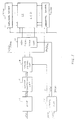
- the driving circuit is what is described in the above-cited Television Institute book and is for driving an active matrix type liquid crystal display device (LCD) depicted at 11.
- LCD liquid crystal display device
- the liquid crystal display device 11 comprises horizontal and vertical pixels which are arranged parallel to two orthogonal coordinate axes, namely, horizontal and vertical axes, as pixel lines or rows and pixel columns in a matrix array.
- Fig. 1 is additionally used in describing a liquid crystal display device driving circuit according to an embodiment of this invention. Fig. 1 is used furthermore in describing a driving circuit according to another embodiment of this invention.
- Such a liquid crystal display device is for displaying a pattern represented by an input video signal V(i) of an input television signal supplied to the driving circuit.
- the input video signal has an analog level variable between 0.0 and 0.7 volt peak to peak.
- horizontal and vertical synchronization signals H(s) and U(s) are supplied to the driving circuit.
- the horizontal synchronization signal defines a horizontal scanning period.
- the vertical synchronization signal defines a vertical scanning period.
- the input video signal V(i) is amplified and level shifted by an amplifier (AMP) 13 into an amplified video signal V(a).
- AMP amplifier
- a gamma conversion circuit 15 converts the amplified video signal into a converted video signal V(c) in accordance with an LCD gamma factor or coefficient ⁇ described hereinabove.
- the amplifier 13 and the gamma conversion circuit 15 are collectively called a video processor.
- a timing circuit 17 From the horizontal and the vertical synchronization signals H(s) and U(s), a timing circuit 17 produces horizontal and vertical scanning pulse sequences H(p) and U(p) and a drive signal control signal F of a horizontal scanning frequency.
- the control signal is for suppressing degradation of the liquid crystal display pixels or elements.
- a drive signal circuit 19 Supplied with the converted video signal V(c) and controlled by the drive signal control signal F, a drive signal circuit 19 produces positive and negative drive signals V(p) and V(n). More particularly, the drive signal circuit 19 is additionally supplied with a predetermined voltage Vcom through a connection (not shown). In case of being supplied with the positive signal from a gamma conversion circuit, inverting the positive drive signal relative to the voltage Vcom in response to the drive signal control signal, the drive signal circuit 19 produces the negative drive signal.
- Horizontal drivers 21 (suffixes omitted) is a shift register having stages operable as pixel line drivers.
- a different shift register is supplied with the vertical scanning pulse sequence U(p) and produces a vertical scan signal for the scanning electrodes to cyclically drive the pixel columns from a column to another.
- the liquid crystal display device 11 is connected to the horizontal drivers 21 and to the vertical scan driver 23.
- the gamma conversion circuit 15 is a conventional digital gamma conversion circuit revdaled in the above-cited Japanese Patent Prepublication No. 220,579 of 1989.
- the digital gamma conversion circuit 15 is for digitally converting the amplified video signal V(a) into the gamma converted video signal V(c) in accordance with the LCD gamma factor.
- an analog-to-digital converter (A/D) 25 converts the amplified video signal into a digital video signal D(v) having digital levels representative of an amplified analog level of the amplified video signal.
- a read only memory (ROM) 27 is preliminarily loaded with a gamma compensation datum between the digital levels and gamma compensated levels into which the digital levels should be converted in accordance with the LCD gamma factor.
- the read only memory 27 Responsive to the digital video signal D(v), the read only memory 27 produces a digital converted signal D(c).
- a digital-to-analog converter (D/A) 29 converts the digital converted signal into an analog converted signal for use as the above-described converted video signal.
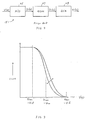
- the luminance versus drive voltage characteristic curves are exemplified with the drive voltage of the positive drive signal V(p).
- the ordinate shows a luminance LUM of light emitted by the liquid crystal display device 11 in response to the drive voltage.
- the luminance is variable between zero and a mximum luminance.
- the drive voltage is varied between zero and about 25 percent of the maximum voltage, the luminance is kept substantially at zero. While the drive voltage is varied between about 90 percent to the maximum voltage, the luminance is kept substantially at the maximum luminance. While the drive voltage is varied between about 25 and about 90 percent, the luminance nonlinearly varies. In the meantime, the luminance linearly varies between about 15 and about 85 percent of the maximum luminance with a slope definining the LCD gamma factor or coefficient while the drive voltage is varied between about 40 and about 70 percent.
- each luminance versus drive voltage characteristic curve is approximated by a nonlinear curve which is generated by a concatenation of first through N-th linear function curves, where N represents an integer which is equal at least to three.
- the gamma factor may slightly differ from a liquid crystal display device to another in the manner indicated by a bidirectionally arrowheaded line.
- an analog gamma conversion or compensation circuit is an analog nonlinear operation circuit for use as the gamma conversion circuit 15 in a liquid crystal display device driving circuit which is according to a first embodiment of this invention and is of the type illustrated with reference to Fig. 1.
- the driving circuit is for driving the liquid crystal display device 11.
- the nonlinear operation circuit comprises first through N-th differential amplifier circuits as first through N-th operation amplifier circuits for generating first through N-th amplifier output signals or first through N-th function voltages in one-to-one correspondence to the first through the N-th linear function curves described in the foregoing and a composing arrangement or unit for composing the first through the N-th amplifier output signals or function voltages into a composite signal. It has been confirmed sufficient that the integer N is equal to three. Such a composite signal is later used as a driving signal in driving the liquid crystal display device 11.
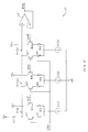
- the analog nonlinear operation circuit comprises first through third differential amplifier circuits 31(1), 31(2) , and 31(3) which will become clear as the description proceeds and have first through third primary input terminals supplied in common with the amplified video signal V(a) described in conjunction with Fig. 1 and first through third secondary input terminals supplied with low, middle, and high reference voltages Vrl (the suffix being a combination of minuscule ar and el), Vrm, and Vrh as first through third reference voltages.
- the amplified video signal may alteratively be referred to simply as an input video signal. It should be noted here that the input video signal has black and white levels.
- the low, the middle, and the high reference voltages are defined by the white level, an intermediate level between the black and the white levels, and the black level.
- the composite signal is a gamma compensated video signal which may be designated by the reference symbol V(c) used before for the converted signal.
- the first differential amplifier circuit 31(1) comprises a first constant current source I(1) for producing a first constant current i(1) .
- a first transistor Q1 has a first base or a first transistor base connected to the first primary input terminal, a first emitter, and a first collector.
- a second transistor Q2 has a second base connected to the first secondary input terminal, a second emitter, and a second collector supplied with a collector or bias voltage Vcc.
- a first resistor R1 has an end connected to the first emitter and another end connected to the first constant current source I(1).
- a second resistor R2 has an end connected to the second emitter and another end connected to the first constant current source I(1).
- the second differential amplifier circuit 31(2) comprises a second constant current source I(2) of a second constant current i(2).
- a third transistor Q3 has a third base connected to the second primary input terminal, a third emitter, and a third collector.
- a fourth transistor Q4 has a fourth base connected to the second secondary input terminal, a fourth emitter, and a fourth collector supplied with the collector voltage.
- a third resistor R3 has an end connected to the third emitter and another end connected to the second constant current source I(2) .
- a fourth resistor R4 has an end connected to the fourth emitter and another end connected to the second constant current source I(2).
- the third differential amplifier circuit 31(3) comprises a third constant current source I(3) for producing a third constant current i(3).
- a fifth transistor Q5 has a fifth base connected to the third primary input terminal, a fifth emitter, and a fifth collector.
- a sixth transistor Q6 has a sixth base connected to the third secondary input terminal, a sixth emitter, and a sixth collector supplied with the collector voltage.
- a fifth resistor R5 has an end connected to the fifth emitter and another end connected to the third constant current source I(3).
- a sixth resistor R6 has an end connected to the sixth emitter and another end connected to the third constant current source I(3).
- the composing arrangement comprises a seventh resistor R7 which has an end connected to the first, the third, and the fifth collectors and another end supplied with electric power of a power voltage Vgc.
- the first through the sixth resistors R1 to R6 are emitter resistors.
- the seventh resistor R7 serves as a load resistor.
- the first through the third differential amplifier circuit 31 (suffixes omitted) produce first through third function voltages collectively as a composite voltage at a common point of connection of the load or seventh resistor R7 to the first, the third, and the fifth collectors.
- An operational amplifier 33 has noninverted or plus and inverted or minus input terminals and an fmplifier output terminal.
- the noninverted input terminal is connected to the common point of connection.
- the inverted input terminal is connected to the amplifier output terminal. Consequently, the operational amplifier 33 serves as a voltage follower for producing the composite signal at the amplifier output terminal as the gamma compensated video signal V(c).
- first and the second resistors R1 and R2 have first and second resistance values R1 and R2 (the same reference symbols being used) which are substantially equal to each other.
- the third and the fourth resistors R3 and R4 have third and fourth resistance values R3 and R4 substantially equal to each other.
- the fifth and the sixth resistors R5 and R6 have fifth and sixth resistance values R5 and R6 substantially equal to each other.
- the seventh resistor R7 has a seventh resistance value R7 which will become shortly clear.
- the input signal V(a) has a first analog level which is equal to the low reference voltage Vrl.
- the first, the second, the fourth, and the sixth transistors Q1, Q2, Q4, and Q6 are in an on state.
- the third and the fifth transistors Q3 and Q5 are in an off state.
- Each of the first and the second transistors Q1 and Q2 is supplied with a half of the constant current i(1)/2.
- the amplified video signal has a slightly raised level.
- a greater current flows through the first transistor Q1 than through the second transistor Q2.
- the first transistor Q1 is supplied with the first constant current i(1).
- the amplified video signal has a second analog level which is equal to the middle reference voltage Vrm.
- the third transistor Q3 is turned into the on state.
- Each of the third and the fourth transistors Q3 and Q4 is supplied with a half of the second constant current i(2)/2.
- Vcm(2) Vgc - R7(i(1) + i(2)).
- the amplifier video signal has a third analog level which is equal to the high reference voltage Vrh.
- the fifth transistor Q5 is switched into the on state.
- Each of the fifth and the sixth transistors Q5 and Q6 is supplied with a half of the third constant current i(3)/2.
- Fig. 5 with Figs. 1 and 4 additionally referred to, the first through the third analog levels of the amplified video signal V(a) are illustrated along the abscissa as equal to the low, the middle, and the high reference voltages Vrl, Vrm, and Vrh.
- the low, the middle, and the high output levels of the gamma compensated video signal V(c) are depicted along the ordinate.
- the gamma compensation circuit 15 of Fig. 4 has an input versus output characteristic curve having a slope defining the LCD gamma factor near the middle reference voltage Vrm or near the middle output level Vcm.
- the drive signal circuit 19 produces the positive drive signal V(p) by inverting the gamma compensated video signal V(c) relative to the predetermined voltage Vcom in the manner indicated in Fig. 5.
- the power source voltage Vgc, the reference voltages Vrl, Vrm, and Vrh, the constant currents i(1) through i(3), and the first through the seventh resistance values R1 to R7 should be set so as to comply with various luminance versus drive voltage characteristic curves having those slopes near the middle reference voltage Vrm which define different LCD gamma factors as exemplified in Fig. 3.
- the second differential amplifier circuit 31(2) comprises first and second MOS transistors M1 and M2 in place of the third and the fourth resistors R3 and R4 (Fig. 4).
- Each of the MOS transistors M (suffixes omitted) has a variable channel resistance controlled by an adjustable gate voltage Vadj.
- the driving circuit is excellently operable. It becomes, however, difficult by the driving circuit being illustrated to drive a liquid crystal display device 11 either by a high definition television signal or by a color television signal. This is because the liquid crystal display device 11 has an enormous number of pixels and because the clock sequence CK must have an accordingly high clock frequency.
- a color video signal comprising red, green, and blue component signals R, G, and B.
- the liquid crystal display device 11 comprises 1280 by 1024 pixels and that the vertical scanning frequency of the drive signal control signal F is 60 Hz. Under the circumstances, the clock frequency is about 108 MHz. Each pixel line or row must be driven within 10 nanoseconds.
- the video processor is supplied with red, green, and blue input video signals V(r), V(g), and V(b) and with the clock sequence CK. It should be known that the red, the green, and the blue video signals are not colored red, green, and blue but that the modifiers "red”, “green”, and “blue” refer to the red, the green, and the blue component signals. This applies to circuit elements and to other signals which will be described in the following.
- a luminance signal is composed of the red, the green, and the blue input video signals in the known manner.
- Black and white levels V(k) and V(w) are derived from the luminance signal.
- the integer N is equal to three. This number of three has no connection with the three primary colors of red, green, and blue.
- the low, the middle, and the high reference voltages Vrl, Vrm, and Vrh are defined by the white level, an intermediate level between the black and the white levels, and the black level.
- the liquid crystal display device is driven by the positive and the negative drive signals and by the horizontal and the vertical scanning pulse sequences.
- the positive and the negative drive signals are derived by combining the predetermined voltage Vcom with the gamma compensated video signal V(c).
- a predetermined number will be represented by M.
- the predetermined number M is typically equal to eight.
- red, green, and blue amplifier circuits (AMP) 35(r), 35(g), and 35(b) amplify and level shift the red, the green, and the blue input video signals or component signals into red, green and blue amplified (video) signals.
- AMP red, green, and blue amplifier circuits
- each of the red, the green, and the blue amplifier circuits 35 is similar in operation to the amplifier 13 described in conjunction with Fig. 1.
- Dividing each of these amplified signals by the predetermined number M, the red, the green, and the blue amplifier circuits 35 produce first through M-th red, green, and blue divided (video) signals.
- the first through the M-th red, green, and blue divided signals are exemplified at V(ar1) to V(ar8), V(ag1) to V(ag8), and V(ab1) to V(ab8).
- Each of red, green, and blue sample and hold (S/H) circuit groups 37(r), 37(g), and 37(b) consists of first through M-th sample and hold circuits.
- each of the first through the M-th sample and hold circuits will be called an m-th sample and hold circuit, where m is variable between 1 and M, both inclusive.
- m-th sample and hold (S/H) circuit of the red sample and hold circuit group 37(r) is illustrated at 37(rm).
- Each of the first through the M-th red divided signals will be referred to as an m-th red divided signal and be denoted by V(arm).
- Figs. 7 and 8 will more particularly be referred to.
- the m-th sample and hold circuits of the red, the green, and the blue sample and hold circuit groups 37 are controlled in common by the clock sequence CK and are supplied with the m-th red, green, and blue divided signals.
- the m-th sample and hold circuits are cyclically operable from the first sample and hold circuit up to the M-th sample and hold circuit.
- the m-th sample and hold circuits of the red, the green, and the blue sample and hold circuit groups 37 hold m-th samples of the red, the green, and the blue divided signals during M pixel clocks to produce red, green, and blue held video signals in the manner exemplified in Fig. 8 by an m-th red held video signal V(srm).
- the red, the green, and the blue sample and hold circuit groups 37 produce first through M-th red, green, and blue held video signals, such as V(sr1) to V(sr8), V(sg1) to V(sg8), and V(sb1) to V(sb8).
- the clock sequence CK has the clock frequency of about 108 MHz.
- the predetermined number M is equal to eight
- the first through the M-th samples of each of the red, the green, and the blue divided signals have a signal width of about 80 nanoseconds.
- the m-th sample is latched about 10 nanoseconds later than an (m-1)-th sample, where the (m-1)-th sample is the M-th sample when the m-th sample is the first sample.
- First and second amplifier circuits (AMP) 39(k) and 39(w) amplify and level shift the black and the white levels V(k) and V(w) of the luminance signal and produce first and second amplified signals A(k) and A(w) .
- Each of the first and the second amplifier circuits 39 (suffixes omitted) is operable similar to the amplifier 13 described in connection with Fig. 1
- First and second sample and hold (S/H) circuits 41(k) and 41(w) are controlled in common by the clock sequence CK and are supplied with the first and the second amplified signals A(k) and A(w).
- the first and the second sample and hold circuits 41 are, although so called, different from the first and the second sample and hold circuits included in the red, the green, and the blue sample and hold circuit groups 37.
- Each of the first and the second sample and hold circuits 41 holds, during the non-displaying period, a sample of one of the first and the second amplified signals that is supplied thereto. In this manner, the first and the second sample and hold circuits 41 produce first and second held signal S(k) and S(w).
- a reference voltage (REF VG) producer 43 produces the low, the middle, and the high reference voltages Vrl, Vrm, and Vrh described before, It is now understood that a combination of the first and the second amplifier circuits 39, the first and the second sample and hold circuits 41, and the reference voltage producer 43 serves as a voltage producing unit for producing the low, the middle, and the high reference voltages in response to the black and the white levels V(k) and V(w) and to the clock sequence CK.
- red, green, and blue analog operation (OP) circuits 45(r), 45(g), and 45(b) are similar to the analog nonlinear operation circuit which is used as the gamma conversion circuit 15 of Fig. 1 in the manner illustrated with reference to Fig. 4.
- the red, the green, and the blue analog operation circuits 45 are therefore three M-channel gamma conversion or compensation circuits and have first through M-th primary red, green, and blue input terminals supplied with the first through the M-th red, green, and blue held video signals V(sr1) to V(sr8), V(sg1) to V(sg8), and V(sb1) to V(sb8) and first through third secondary red, green, and blue input terminals supplied, as the first through the third reference voltages, with the low, the middle, and the high reference voltages from the voltage producing unit (39, 41, 43).
- the red, the green, and the blue analog operation circuits 45 nonlinearly process the first through the M-th red, green, and blue held video signals into first through M-th red, green, and blue gamma compensated signals, such as V(cr1) to V(cr8), V(cg1) to V(cg8), and V(cb1) to V(cb8).
- V(cr1) to V(cr8), V(cg1) to V(cg8), and V(cb1) to V(cb8) V(cr1) to V(cr8), V(cg1) to V(cg8), and V(cb1) to V(cb8).
- the first through the M-th red, green, and blue gamma compensated signals are delivered to the drive signal circuit 19 illustrated in Fig. 1.
- the red, the green, and the blue analog operation circuits 45 will be reviewed. Although the samples are latched during different time intervals, the first through the M-th sample and hold circuits of the red, the green, and the blue sample and hold circuit groups 37 and the first and the second sample and hold circuits 41 have a common structure of common circuit elements to be operable with a substantially common offset voltage. As a consequence, the low, the middle, and the high reference voltages have a common voltage relationship to the first through the M-th red, green, and blue held video signals and the first and the second held signals. This makes it possible for the red, the green, and the blue analog operation circuits 45 to correctly compensate for the LCD gamma factor.
- a combination of the amplifier circuits 35, the sample and hold circuit groups 37, and the analog operation circuits 45 is operable as the video processor (13, 15) mentioned in conjunction with Fig. 1.
- the voltage producing unit may be included in the gamma conversion circuit 15 and consequently in the video processor.
- each of these circuits 45 consists of M-channel gamma compensation circuits, namely, of first through M-th unit analog operation circuits, each of which is a single analog nonlinear operation circuit.
- M-channel gamma compensation circuits namely, of first through M-th unit analog operation circuits, each of which is a single analog nonlinear operation circuit.
- one of the first through the M-th red, green, and blue video signals may be called a single video signal.
- the single analog operation circuit is supplied with the low, the middle, and the high reference voltages at the first through the third secondary input terminals.
- the single video signal is supplied in common to the first through the third primary input terminals of the single analog operation circuit in place of the amplified video signal V(a) described with reference to Figs. 1 and 4.
- the video processor should comprise, among the circuit elements illustrated with reference to Fig. 7, one of the red, the green, and the blue amplifier circuits 35, a pertinent one of the red, the green, and the blue sample and hold circuit groups 37, a relevent one of the red, the green, and the blue analog operation circuits 45, and the voltage producing unit (39, 41, 43). It is possible in this event to understand that this circuitry is an equivalent of the circuitry illustrated with reference to Fig. 7.
Landscapes
- Physics & Mathematics (AREA)
- Crystallography & Structural Chemistry (AREA)
- Engineering & Computer Science (AREA)
- Multimedia (AREA)
- Signal Processing (AREA)
- Chemical & Material Sciences (AREA)
- Nonlinear Science (AREA)
- Mathematical Physics (AREA)
- General Physics & Mathematics (AREA)
- Optics & Photonics (AREA)
- Transforming Electric Information Into Light Information (AREA)
- Liquid Crystal Display Device Control (AREA)
- Video Image Reproduction Devices For Color Tv Systems (AREA)
- Picture Signal Circuits (AREA)
Applications Claiming Priority (3)
| Application Number | Priority Date | Filing Date | Title |
|---|---|---|---|
| JP16893 | 1993-01-05 | ||
| JP5000168A JP3071590B2 (ja) | 1993-01-05 | 1993-01-05 | 液晶ディスプレイ装置 |
| JP168/93 | 1993-01-05 |
Publications (3)
| Publication Number | Publication Date |
|---|---|
| EP0606061A2 true EP0606061A2 (fr) | 1994-07-13 |
| EP0606061A3 EP0606061A3 (fr) | 1995-11-02 |
| EP0606061B1 EP0606061B1 (fr) | 1999-12-08 |
Family
ID=11466502
Family Applications (1)
| Application Number | Title | Priority Date | Filing Date |
|---|---|---|---|
| EP94100025A Expired - Lifetime EP0606061B1 (fr) | 1993-01-05 | 1994-01-03 | Circuit analogique produisant une caractéristique luminance/tension de commande non-linéaire, pour dispositifs d'affichage à cristaux liquides |
Country Status (5)
| Country | Link |
|---|---|
| US (1) | US5483256A (fr) |
| EP (1) | EP0606061B1 (fr) |
| JP (1) | JP3071590B2 (fr) |
| KR (1) | KR0170003B1 (fr) |
| DE (1) | DE69421946T2 (fr) |
Cited By (3)
| Publication number | Priority date | Publication date | Assignee | Title |
|---|---|---|---|---|
| WO1996037073A1 (fr) * | 1995-05-18 | 1996-11-21 | Polaroid Corporation | Circuit de traitement de signaux video |
| CN1322485C (zh) * | 2002-12-11 | 2007-06-20 | Lg.飞利浦Lcd有限公司 | 产生伽马电压的装置和方法 |
| EP2258044A1 (fr) * | 2008-03-25 | 2010-12-08 | QUALCOMM Incorporated | Système et procédé permettant de réaliser une opération de compression-extension sur un signal d'entrée d'un récepteur à détection d'énergie |
Families Citing this family (21)
| Publication number | Priority date | Publication date | Assignee | Title |
|---|---|---|---|---|
| JP3202450B2 (ja) * | 1993-10-20 | 2001-08-27 | 日本電気株式会社 | 液晶表示装置 |
| JP2708380B2 (ja) * | 1994-09-05 | 1998-02-04 | インターナショナル・ビジネス・マシーンズ・コーポレイション | ガンマ補正を行うディジタル・アナログ変換装置及び液晶表示装置 |
| JP2713193B2 (ja) * | 1994-12-19 | 1998-02-16 | 日本電気株式会社 | γ補正回路 |
| KR960024524A (ko) * | 1994-12-21 | 1996-07-20 | 김광호 | 기억소자를 이용한 액정 표시장치의 감마 보정장치 |
| US5905540A (en) * | 1994-12-27 | 1999-05-18 | Seiko Epson Corporation | Projection-type display apparatus |
| JP3199978B2 (ja) * | 1995-03-31 | 2001-08-20 | シャープ株式会社 | 液晶表示装置 |
| WO1998048317A1 (fr) * | 1997-04-18 | 1998-10-29 | Seiko Epson Corporation | Circuit et procede d'attaque d'un dispositif electro-optique, dispositif electro-optique et equipement electronique obtenu a l'aide dudit dispositif |
| JP3148151B2 (ja) * | 1997-05-27 | 2001-03-19 | 日本電気株式会社 | 液晶駆動装置の出力偏差低減方法および装置 |
| JPH11143379A (ja) * | 1997-09-03 | 1999-05-28 | Semiconductor Energy Lab Co Ltd | 半導体表示装置補正システムおよび半導体表示装置の補正方法 |
| JP2000022988A (ja) * | 1998-07-06 | 2000-01-21 | Sony Corp | ガンマ補正回路 |
| AU739565B2 (en) * | 1998-10-06 | 2001-10-18 | Matsushita Electric Industrial Co., Ltd. | Gamma correction circuit and gamma correction method |
| JP2000134507A (ja) * | 1998-10-21 | 2000-05-12 | Sony Corp | ガンマ補正回路 |
| US6441870B1 (en) * | 1998-12-22 | 2002-08-27 | Gateway, Inc. | Automatic gamma correction for multiple video sources |
| JP3412583B2 (ja) | 1999-11-08 | 2003-06-03 | 日本電気株式会社 | カラー液晶ディスプレイの駆動方法及びその回路 |
| US7170478B2 (en) * | 2002-03-26 | 2007-01-30 | Semiconductor Energy Laboratory Co., Ltd. | Method of driving light-emitting device |
| KR20040041940A (ko) * | 2002-11-12 | 2004-05-20 | 삼성전자주식회사 | 액정 표시 장치 및 그 구동 방법 |
| KR100934826B1 (ko) * | 2003-10-21 | 2009-12-31 | 엘지디스플레이 주식회사 | 액정 표시소자의 감마 기준전압 설정방법 |
| TWI233073B (en) * | 2003-12-04 | 2005-05-21 | Au Optronics Corp | Programmable gamma circuit and display apparatus |
| TW200727227A (en) * | 2006-01-10 | 2007-07-16 | Compal Electronics Inc | Gamma curve compensating device and method use the same |
| JP2016186633A (ja) * | 2016-04-25 | 2016-10-27 | 株式会社半導体エネルギー研究所 | 半導体装置及び電子機器 |
| US12374306B1 (en) | 2022-06-22 | 2025-07-29 | Apple Inc. | Display column driver devices with offset cancellation |
Family Cites Families (11)
| Publication number | Priority date | Publication date | Assignee | Title |
|---|---|---|---|---|
| US3708693A (en) * | 1971-05-19 | 1973-01-02 | Ferrex Corp | Gamma corrector |
| JPS57201295A (en) * | 1981-06-04 | 1982-12-09 | Sony Corp | Two-dimensional address device |
| US4499494A (en) * | 1982-09-27 | 1985-02-12 | Rca Corporation | Television gamma corrector with symmetrical response about black-level |
| JPS60257674A (ja) * | 1984-06-04 | 1985-12-19 | Olympus Optical Co Ltd | 広帯域ガンマ補正回路 |
| EP0235862B1 (fr) * | 1986-03-07 | 1991-11-06 | Koninklijke Philips Electronics N.V. | Circuit de correction gamma |
| EP0275140B1 (fr) * | 1987-01-09 | 1995-07-19 | Hitachi, Ltd. | Méthode et dispositif de balayage de charges capacitives |
| JPH0334788A (ja) * | 1989-06-30 | 1991-02-14 | Sharp Corp | ガンマ補正回路 |
| JP2554955B2 (ja) * | 1990-10-02 | 1996-11-20 | 池上通信機株式会社 | 非線形処理回路 |
| JPH04258018A (ja) * | 1991-02-13 | 1992-09-14 | Nec Corp | 振幅変換回路 |
| JPH04271577A (ja) * | 1991-02-27 | 1992-09-28 | Toshiba Corp | 液晶表示装置のガンマ補正方式 |
| JP2774881B2 (ja) * | 1991-07-26 | 1998-07-09 | シャープ株式会社 | ガンマ補正回路 |
-
1993
- 1993-01-05 JP JP5000168A patent/JP3071590B2/ja not_active Expired - Lifetime
-
1994
- 1994-01-03 EP EP94100025A patent/EP0606061B1/fr not_active Expired - Lifetime
- 1994-01-03 DE DE69421946T patent/DE69421946T2/de not_active Expired - Lifetime
- 1994-01-04 KR KR1019940000062A patent/KR0170003B1/ko not_active Expired - Lifetime
-
1995
- 1995-02-27 US US08/395,145 patent/US5483256A/en not_active Expired - Lifetime
Cited By (3)
| Publication number | Priority date | Publication date | Assignee | Title |
|---|---|---|---|---|
| WO1996037073A1 (fr) * | 1995-05-18 | 1996-11-21 | Polaroid Corporation | Circuit de traitement de signaux video |
| CN1322485C (zh) * | 2002-12-11 | 2007-06-20 | Lg.飞利浦Lcd有限公司 | 产生伽马电压的装置和方法 |
| EP2258044A1 (fr) * | 2008-03-25 | 2010-12-08 | QUALCOMM Incorporated | Système et procédé permettant de réaliser une opération de compression-extension sur un signal d'entrée d'un récepteur à détection d'énergie |
Also Published As
| Publication number | Publication date |
|---|---|
| EP0606061A3 (fr) | 1995-11-02 |
| KR940018689A (ko) | 1994-08-18 |
| DE69421946T2 (de) | 2000-07-20 |
| US5483256A (en) | 1996-01-09 |
| KR0170003B1 (ko) | 1999-03-20 |
| JPH06205340A (ja) | 1994-07-22 |
| JP3071590B2 (ja) | 2000-07-31 |
| DE69421946D1 (de) | 2000-01-13 |
| EP0606061B1 (fr) | 1999-12-08 |
Similar Documents
| Publication | Publication Date | Title |
|---|---|---|
| US5483256A (en) | LCD driving analog nonlinear operation circuit producing a composite drive voltage of function voltages of differential amplifiers | |
| US8698720B2 (en) | Display signal processing device and display device | |
| KR100506463B1 (ko) | 칼러액정표시의 구동회로 및 구동방법, 및 칼러액정표시장치 | |
| US7298352B2 (en) | Apparatus and method for correcting gamma voltage and video data in liquid crystal display | |
| US6879310B2 (en) | Liquid crystal display and method for driving the same | |
| CN101414447B (zh) | 驱动电路装置 | |
| US11120772B1 (en) | Source driving circuit, display apparatus and operation method of display apparatus | |
| KR20010051546A (ko) | 컬러액정디스플레이를 위한 구동방법 및 구동회로 | |
| US7193550B2 (en) | Driving circuit of flat display device, and flat display device | |
| JP2008122960A (ja) | 表示装置及びその駆動装置 | |
| CN115798378B (zh) | 显示装置及其显示方法 | |
| US11741915B2 (en) | Display driver suppressing color unevenness of liquid crystal display | |
| KR102435875B1 (ko) | 하이 다이내믹 레인지 영상 신호 처리를 위한 구동 회로 및 그것을 포함하는 표시 장치 | |
| JPH02271390A (ja) | 液晶表示装置 | |
| EP1727113A1 (fr) | Ecran et methode d affichage | |
| US7289094B2 (en) | Device circuit for flat display apparatus and flat display apparatus | |
| KR100251151B1 (ko) | 디스플레이소자의비선형특성보정장치및그보정방법 | |
| KR100672621B1 (ko) | 액정표시장치의 구동회로 | |
| JP3251487B2 (ja) | 画像処理装置 | |
| US8159509B2 (en) | Color display device and method for reproducing color with an increased number of gradation levels | |
| EP1538595B1 (fr) | Circuit de commande pour un dispositif d'affichage à cristaux liquides et son procédé de commande | |
| EP1274230A2 (fr) | Circuit de contrôle du niveau de suppression et méthode de contrôle du niveau de suppression | |
| US5889503A (en) | Signal processing circuit and liquid crystal display apparatus using the same circuit | |
| EP1094434A1 (fr) | Dispostif d'affichage avec dégradation de la matière fluorescente uniforme et méthode correspondente | |
| US6809712B2 (en) | Drive circuit of liquid crystal display, having clip circuit before polarity inversion circuit |
Legal Events
| Date | Code | Title | Description |
|---|---|---|---|
| PUAI | Public reference made under article 153(3) epc to a published international application that has entered the european phase |
Free format text: ORIGINAL CODE: 0009012 |
|
| AK | Designated contracting states |
Kind code of ref document: A2 Designated state(s): DE FR GB |
|
| PUAL | Search report despatched |
Free format text: ORIGINAL CODE: 0009013 |
|
| AK | Designated contracting states |
Kind code of ref document: A3 Designated state(s): DE FR GB |
|
| 17P | Request for examination filed |
Effective date: 19960213 |
|
| 17Q | First examination report despatched |
Effective date: 19970424 |
|
| GRAG | Despatch of communication of intention to grant |
Free format text: ORIGINAL CODE: EPIDOS AGRA |
|
| GRAG | Despatch of communication of intention to grant |
Free format text: ORIGINAL CODE: EPIDOS AGRA |
|
| GRAH | Despatch of communication of intention to grant a patent |
Free format text: ORIGINAL CODE: EPIDOS IGRA |
|
| GRAH | Despatch of communication of intention to grant a patent |
Free format text: ORIGINAL CODE: EPIDOS IGRA |
|
| GRAA | (expected) grant |
Free format text: ORIGINAL CODE: 0009210 |
|
| AK | Designated contracting states |
Kind code of ref document: B1 Designated state(s): DE FR GB |
|
| REF | Corresponds to: |
Ref document number: 69421946 Country of ref document: DE Date of ref document: 20000113 |
|
| ET | Fr: translation filed | ||
| PLBE | No opposition filed within time limit |
Free format text: ORIGINAL CODE: 0009261 |
|
| STAA | Information on the status of an ep patent application or granted ep patent |
Free format text: STATUS: NO OPPOSITION FILED WITHIN TIME LIMIT |
|
| 26N | No opposition filed | ||
| REG | Reference to a national code |
Ref country code: GB Ref legal event code: IF02 |
|
| REG | Reference to a national code |
Ref country code: GB Ref legal event code: 732E |
|
| REG | Reference to a national code |
Ref country code: FR Ref legal event code: TP |
|
| REG | Reference to a national code |
Ref country code: DE Ref legal event code: R082 Ref document number: 69421946 Country of ref document: DE Representative=s name: BETTEN & RESCH PATENT- UND RECHTSANWAELTE PART, DE Effective date: 20110919 Ref country code: DE Ref legal event code: R082 Ref document number: 69421946 Country of ref document: DE Representative=s name: PATENTANWAELTE BETTEN & RESCH, DE Effective date: 20110919 Ref country code: DE Ref legal event code: R081 Ref document number: 69421946 Country of ref document: DE Owner name: NLT TECHNOLOGIES, LTD., KAWASAKI, JP Free format text: FORMER OWNER: NEC LCD TECHNOLOGIES, LTD., KAWASAKI, KANAGAWA, JP Effective date: 20110919 Ref country code: DE Ref legal event code: R081 Ref document number: 69421946 Country of ref document: DE Owner name: NLT TECHNOLOGIES, LTD., JP Free format text: FORMER OWNER: NEC LCD TECHNOLOGIES, LTD., KAWASAKI, JP Effective date: 20110919 |
|
| REG | Reference to a national code |
Ref country code: FR Ref legal event code: CD Owner name: NLT TECHNOLOGIES, LTD, JP Effective date: 20111013 Ref country code: FR Ref legal event code: CA Effective date: 20111013 |
|
| PGFP | Annual fee paid to national office [announced via postgrant information from national office to epo] |
Ref country code: FR Payment date: 20130204 Year of fee payment: 20 Ref country code: DE Payment date: 20121231 Year of fee payment: 20 Ref country code: GB Payment date: 20130102 Year of fee payment: 20 |
|
| REG | Reference to a national code |
Ref country code: DE Ref legal event code: R071 Ref document number: 69421946 Country of ref document: DE |
|
| REG | Reference to a national code |
Ref country code: DE Ref legal event code: R071 Ref document number: 69421946 Country of ref document: DE |
|
| REG | Reference to a national code |
Ref country code: GB Ref legal event code: PE20 Expiry date: 20140102 |
|
| PG25 | Lapsed in a contracting state [announced via postgrant information from national office to epo] |
Ref country code: GB Free format text: LAPSE BECAUSE OF EXPIRATION OF PROTECTION Effective date: 20140102 |
|
| PG25 | Lapsed in a contracting state [announced via postgrant information from national office to epo] |
Ref country code: DE Free format text: LAPSE BECAUSE OF EXPIRATION OF PROTECTION Effective date: 20140104 |