EP0606655A1 - Halbleiterscheiben-Speicherkassette Apparat und Transfereinrichtung für direkte Ladung und Entladung - Google Patents
Halbleiterscheiben-Speicherkassette Apparat und Transfereinrichtung für direkte Ladung und Entladung Download PDFInfo
- Publication number
- EP0606655A1 EP0606655A1 EP93121116A EP93121116A EP0606655A1 EP 0606655 A1 EP0606655 A1 EP 0606655A1 EP 93121116 A EP93121116 A EP 93121116A EP 93121116 A EP93121116 A EP 93121116A EP 0606655 A1 EP0606655 A1 EP 0606655A1
- Authority
- EP
- European Patent Office
- Prior art keywords
- wafer
- cassette
- wafers
- robot
- recited
- Prior art date
- Legal status (The legal status is an assumption and is not a legal conclusion. Google has not performed a legal analysis and makes no representation as to the accuracy of the status listed.)
- Granted
Links
Images
Classifications
-
- H—ELECTRICITY
- H10—SEMICONDUCTOR DEVICES; ELECTRIC SOLID-STATE DEVICES NOT OTHERWISE PROVIDED FOR
- H10P—GENERIC PROCESSES OR APPARATUS FOR THE MANUFACTURE OR TREATMENT OF DEVICES COVERED BY CLASS H10
- H10P72/00—Handling or holding of wafers, substrates or devices during manufacture or treatment thereof
- H10P72/10—Handling or holding of wafers, substrates or devices during manufacture or treatment thereof using carriers specially adapted therefor, e.g. front opening unified pods [FOUP]
- H10P72/14—Vertical carrier comprising wall type elements whereby the substrates are horizontally supported, e.g. comprising sidewalls
-
- H—ELECTRICITY
- H10—SEMICONDUCTOR DEVICES; ELECTRIC SOLID-STATE DEVICES NOT OTHERWISE PROVIDED FOR
- H10P—GENERIC PROCESSES OR APPARATUS FOR THE MANUFACTURE OR TREATMENT OF DEVICES COVERED BY CLASS H10
- H10P72/00—Handling or holding of wafers, substrates or devices during manufacture or treatment thereof
- H10P72/30—Handling or holding of wafers, substrates or devices during manufacture or treatment thereof for conveying, e.g. between different workstations
- H10P72/34—Handling or holding of wafers, substrates or devices during manufacture or treatment thereof for conveying, e.g. between different workstations the wafers being stored in a carrier, involving loading and unloading
- H10P72/3402—Mechanical parts of transfer devices
-
- H—ELECTRICITY
- H10—SEMICONDUCTOR DEVICES; ELECTRIC SOLID-STATE DEVICES NOT OTHERWISE PROVIDED FOR
- H10P—GENERIC PROCESSES OR APPARATUS FOR THE MANUFACTURE OR TREATMENT OF DEVICES COVERED BY CLASS H10
- H10P72/00—Handling or holding of wafers, substrates or devices during manufacture or treatment thereof
- H10P72/30—Handling or holding of wafers, substrates or devices during manufacture or treatment thereof for conveying, e.g. between different workstations
- H10P72/34—Handling or holding of wafers, substrates or devices during manufacture or treatment thereof for conveying, e.g. between different workstations the wafers being stored in a carrier, involving loading and unloading
- H10P72/3411—Handling or holding of wafers, substrates or devices during manufacture or treatment thereof for conveying, e.g. between different workstations the wafers being stored in a carrier, involving loading and unloading involving loading and unloading of wafers
-
- Y—GENERAL TAGGING OF NEW TECHNOLOGICAL DEVELOPMENTS; GENERAL TAGGING OF CROSS-SECTIONAL TECHNOLOGIES SPANNING OVER SEVERAL SECTIONS OF THE IPC; TECHNICAL SUBJECTS COVERED BY FORMER USPC CROSS-REFERENCE ART COLLECTIONS [XRACs] AND DIGESTS
- Y10—TECHNICAL SUBJECTS COVERED BY FORMER USPC
- Y10S—TECHNICAL SUBJECTS COVERED BY FORMER USPC CROSS-REFERENCE ART COLLECTIONS [XRACs] AND DIGESTS
- Y10S414/00—Material or article handling
- Y10S414/135—Associated with semiconductor wafer handling
- Y10S414/137—Associated with semiconductor wafer handling including means for charging or discharging wafer cassette
-
- Y—GENERAL TAGGING OF NEW TECHNOLOGICAL DEVELOPMENTS; GENERAL TAGGING OF CROSS-SECTIONAL TECHNOLOGIES SPANNING OVER SEVERAL SECTIONS OF THE IPC; TECHNICAL SUBJECTS COVERED BY FORMER USPC CROSS-REFERENCE ART COLLECTIONS [XRACs] AND DIGESTS
- Y10—TECHNICAL SUBJECTS COVERED BY FORMER USPC
- Y10S—TECHNICAL SUBJECTS COVERED BY FORMER USPC CROSS-REFERENCE ART COLLECTIONS [XRACs] AND DIGESTS
- Y10S414/00—Material or article handling
- Y10S414/135—Associated with semiconductor wafer handling
- Y10S414/139—Associated with semiconductor wafer handling including wafer charging or discharging means for vacuum chamber
Definitions
- This invention relates to a semiconductor wafer cassette and wafer transfer system for the temporary storage and transfer of semiconductor wafers during the manufacturing process; and more particularly, to a semiconductor wafer cassette apparatus and associated transfer system which is capable of directly loading and unloading wafers into the cassette from different sides using a first robot handling means having a wafer transfer blade movable along a first extension path and a second robot handling means having a second wafer transfer blade movable along a second extension path intersecting the first extension path at an acute angle and at a predetermined point concurrent with the cassette's wafer position centerline.
- a plurality of wafers are temporarily stored and transferred between manufacturing and processing apparatus locations in factory cassettes.
- the factory cassette is either manually or automatically loaded into a loadlock chamber of the processing apparatus wherefrom the wafers may be unloaded for processing, or a factory robot unloads the wafers individually from the factory cassette and loads them into a fixed temporary storage cassette positioned in the loadlock chamber.
- the cassette In the former case, where the factory cassette is manually loaded, the cassette is typically accessible from one side only and is oriented so that the system robot can access the wafer directly along an extension path directed perpendicular to the accessible side of the cassette.
- the cassette In the latter case, where a factory robot loads and unloads individual wafers between a factory cassette and a fixed cassette positioned in the loadlock chamber, the cassette is accessible from different sides, i.e., it is a "pass-through" cassette.
- the pass-through cassette can be directly accessed by both the factory robot and the system robot if both robots are disposed in a position such that the extension path of each robot arm is along a common axis directed perpendicular to the accessible sides of the pass-through cassette.
- the pass-through type of cassette is preferred over the cassettes having only one accessible side because it enables efficient robotic wafer handling, both inside and outside of the processing apparatus.
- a processing apparatus having a plurality of loadlock chambers for accommodating simultaneous loading/unloading operations by both the factory robot and the system robot.
- multiple loadlock chambers are positioned about a generally cylindrical, (multi-faced) wafer transfer chamber having a "simple" R-theta type robot (i.e., a robot having two degrees of freedom, one in extension/retraction and one in rotation) disposed therein.
- a simple R-theta robot is preferred so that it can rotate and load/unload wafers from any processing chamber disposed about the periphery of the transfer chamber.
- One solution to this problem is to provide a means for orienting the pass-through cassette once loaded, i.e., rotate the cassette, so that it can be accessed on one side along the extension path of the R-theta robot and on the other side along the extension path of the factory robot.
- providing such an orientation means adds undesirable complexity and cost to the system.
- a semiconductor wafer transfer system which includes a pass-through-type wafer cassette disposed within a plurality of loadlock chambers positioned about the periphery of a generally circular transfer chamber having an R-theta robot (without articulated arm), and which can be directly loaded/unloaded from one side by a factory robot and from a different side by a system R-theta robot, the two robots having extension paths intersecting at an acute angle.
- a semiconductor wafer cassette for the temporary storage of one or more semiconductor wafers.
- the cassette can be loaded/unloaded by a first robot blade moveable in a first direction between two wafer supports, and loaded/unloaded by a second robot blade moveable in a second direction, said first and second directions intersecting at an acute angle at the center of the cassette.
- the cassette is comprised of a pair of wafer supports having shelves thereon for supporting a plurality of wafers, the pair of supports distanced and placed such that wafers are supported and the robot blades can be inserted between them for loading and unloading wafers.
- the cassette is useful in combination with one or more loadlock chambers in a wafer processing system.
- the loadlock chamber has an opening for access by the first robot blade, and a second opening for access by a system robot that can unload wafers from the cassette and transfer them to one or more processing chambers, and reload the wafers into the cassette.
- the first robot blade can unload the processed wafers from the system.
- the cassettes of the invention are advantageous because they can be employed with a factory robot external to the wafer processing system, and a simple R-theta system robot, avoiding the need for elaborate and more expensive articulated arm robots.
- a further advantage of the cassettes of the invention comprises supporting shelves which have stepped edges for handling wafers of different sizes and for retention of wafers that are slightly misaligned with respect to the robot blades.
- the supporting steps maintain the position of the wafers and eliminate the need to provide precise and expensive wafer center-finding equipment prior to loading/unloading wafers.
- the robot blades can also be fitted with a like series of stepped edges which reduce the amount of wafer movement possible during loading/unloading operations, even if the wafer is misaligned with respect to the blade.
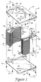
- the cassette (“pass-through cassette") 10 of this invention is shown in exploded perspective view, comprising a first wafer support 13 , a second wafer support 15 , a top plate 17 including an optionally attachable carrying handle 19 , and a bottom plate 21 . All of these individual parts are preferably made of a metal alloy, but may also be made of formed plastic.
- Both the first and second wafer supports 13 and 15 of this invention include a plurality of integrally formed wafer support shelves 23 , raised mounting shoulders 25 and downwardly extending mounting feet 27 .
- Each wafer support shelf 23 includes a series of integrally formed steps ("stepped shoulders") 29a-c for the positioning and retention of individual wafers 31 thereon.
- Each of the shoulders 25 and feet 27 have drilled, threaded holes 33 and alignment dowels 35 for proper alignment and attachment to outwardly extending fastening extensions 38 of the top and bottom plates 17 and 21 .
- Each extension is provided with drilled dowel alignment holes 37 and fastening holes 39 .
- Plates 17 and 21 also include integrally formed downwardly extending ribs 43 that serve as standoffs and provide underside clearance 45 when the plates 17 and 21 are fastened to the wafer supports 13 and 15 . Plates 17 and 21 are fastened to the wafer supports 13 and 15 by flush mounting screws 41 .
- positioning holes 20 are drilled through the top plate 17 and the carry handle 19 is attached by flush mounting screws 18 .
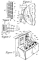
- Fig. 2 of the accompanying drawings there is shown a plan view of the second wafer support 15 shown in Fig. 1 .
- the first wafer support 13 is substantially identical in configuration to the second wafer support 15 illustrated in Fig. 2 .
- the first wafer support 13 is not shown in the same individual detail herein.
- the position and arcuate shelf lengths of the wafer supports 13 and 15 depend upon the known diameter 32 of the wafer 31 to be loaded onto the wafer support shelves 23 , the known widths 75a and 77 of the wafer-carrying blades 59a and 54 , and the intersection angle ⁇ of the axes 69 and 71a of the extension travel paths of the wafer-carryingblades 54 and 59a .
- the arcuate lengths of the shelves 29 are dimensioned so that the supports do not interfere with the blades 59a and 54 when they are extended during the loading and unloading of the cassette 10 . As may be geometrically determined from the layout depicted in Fig.
- the arcuate shelves 29 must be configured to subtend angles "S" of less than where is the angle of intersection of the axes 69 and 71a , W1 is the width 77 of blade 54 , W2 is the width 75a of blade 59a , and r is the radius of a wafer to be loaded into cassette 10 .
- the inner edge 47 of the wafer support shelf 23 and the shoulders forming wafer support steps 29a , 29b and 29c are arcuately formed to be concentric with the circumference of a particular size of wafer having a diameter 32 .
- Innermost step 29a is of a dimension to support the wafer 31 in its centered position, as illustrated in Fig. 2 . In the event, however, that a wafer 31 is not centrally loaded within the cassette 10 , the wafer 31 can still be supported by the innermost step 29a and either step 29b or 29c , depending on how far offset the wafer 31 is from the center of the cassette 10 when it is loaded.
- a partial cross-section of the wafer support of Fig. 2 is depicted looking in the direction of the arrows 3-3.
- the riser and plurality of shelves can be formed of a combination of parts or can be machined or otherwise crafted from a single body of material.
- each shelf includes wafer support steps 29a , 29b and 29c .
- a centered wafer will rest upon the first step 29a as indicated by the dashed lines 31a , while a slightly off-centered wafer, such as that represented by the dashed lines 31b , might rest on the step 29b . In either case, further lateral movement away from the centered position will be restrained by engagement of the wafer edge with a step riser.
- a wafer 31 can be substantially off-center when loaded into the cassette 10 and yet be supported and restrained from movement away from the central position. In fact, movement or vibration of the cassette will tend to cause the wafer to move toward the centered position as it slips from one step to another. This feature thus reduces and/or eliminates the need for any precise wafer centering prior to loading of the cassette.
- Fig. 4 of the accompanying drawing a side elevational view of wafer support 13 is shown looking in the direction of the arrows 4-4 of Fig. 1 .
- Fig 4 illustrates the unitary construction of the wafer supports, including the plurality of identically formed wafer support shelves 23 , a riser 26 terminating at the top in a raised mounting shoulder 25 and at the bottom in a downward extending mounting foot 27 , and alignment dowels 35 .
- FIG. 5 illustrates a first robot means ("factory robot") 53 which is positioned in an ambient environment between a row of factory cassettes 51 supported on a housing extension 49 and the outer perimeter wall 55a of the processing apparatus 55 .
- the factory cassettes 51 each contain a plurality of wafers accessible for loading/unloading by factory robot 53 .
- the factory robot 53 is capable of linear movement in the direction of arrow 53a which is substantially parallel to the supply row of factory cassettes 51 and the perimeter wall 55a of the processing apparatus 55 .
- the processing apparatus 55 includes dual loadlock access ports 56a and 56b through which the factory robot 53 loads and/or unloads the cassette 10 of the invention disposed within the loadlock chambers 61a and 61b (see Fig. 6 ).
- the factory robot 53 is shown inserting a wafer 31 through the open port 56b into loadlock chamber 61b ( Fig. 6 ) for transfer to the cassette 10 .
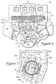
- FIG. 6 a partially broken plan view of the wafer support and transfer system 46 of this invention and the processing apparatus 55 .
- Factory robot 53 is shown unloaded with its wafer support blade 54 in a retracted position.
- the apparatus 55 includes a low pressure central wafer transfer chamber 57 and an R-theta system robot 59 positioned therein.
- First and second wafer loadlock chambers 61a and 61b are positioned about the periphery of chamber 57
- first and second cassettes 10 are respectively positioned in first and second loadlock chambers 61a and 61b .
- a pair of wafer processing chambers 65 and 67 are also shown located about the periphery of chamber 57 .
- the R-theta robot 59 rotates about its centerpoint 59b in the direction of the arrow 72 and includes arms 60 which carry the wafer support blade 59a and extend and retract it radially, in the direction of the arrows 60a , for loading and unloading the wafers 31 to and from the cassettes 31 and chambers 65 and 67 .
- FIG. 6 Also illustrated in Fig. 6 is the linear travel path axis 70 and lateral extension path axes 69 of the factory robot 53 .
- the factory robot's extension axes 69 are substantially normal to the robot's linear travel axis 70 and the loadlock chamber access ports 56a and 56b .
- the inner sides 63a and 63b of loadlock chambers 61a and 61b (comprising an access way between loadlock chambers 61a and 61b and the central transfer chamber 57 along R-theta system robot extension pathways) are oriented substantially tangential to the central position of the R-theta system robot 59 and transverse to the system robots extension path axes 71a and 71b .
- the wafer support and transfer system 46 of this invention comprising the factory robot 53 , the R-theta robot 59 , and the cassettes 10 disposed within loadlock chambers 61a and 61b , differs from the prior art methods by permitting the direct loading and/or unloading of wafers 31 along robot extension paths 69 , 71a and 71b which intersect at an acute angle ⁇ .
- Fig. 7 of the accompanying drawings there is shown for illustration purposes an enlarged plan view of the loadlock chamber 61a of Fig. 6 with the cassette 10 therein, and both the factory robot wafer support blade 54 and the R-theta system robot wafer support blade 59a shown in their extended (loading and unloading) positions.
- the wafer supports 13 and 15 of the cassette 10 are positioned in loadlock chamber 61a so that the centerpoint 73 of the cassette 10 is concurrent with the wafer position centerpoints 75 of the robot blades 54 and 59a .
- the centerpoint 73 also corresponds with the point of intersection of the factory robot extension axis 69 and the R-theta system robot extension axis 71a .
- the wafer supports 13 and 15 are oriented so that the robot blades 54 and 59 , when at their extended position as shown, do not strike the wafer support shelves 23 ( Fig. 1 ) of the wafer supports 13 and 15 during wafer loading and/or unloading from either side of the cassette 10 .
- the blades 59a and 54 also have wafer support steps 79a-c ("stepped shoulders") like those of the wafer support shelves 23 of the wafer supports 13 and 15 for the purpose of limiting the movement of wafers 31 during loading and unloading.
- the position of cassette 10 (and the locations of wafer supports 13 and 15 ) in the loadlock chamber 61a is determined by the point of intersection 73 of the extension axes 69 and 71a of the blades 54 and 59a and the acute angle ⁇ formed thereby.
- the loadlock chambers may be of any design configuration subject to the limitation that there be sufficient travel clearance between the side walls 81a and 81b and the wafer as it is loaded and unloaded from the cassette 10 by the factory and system robot blades 54 and 59a .
- the present invention is also advantageous in that it can be readily retrofit to existing wafer processing apparatus with little expense.
Landscapes
- Container, Conveyance, Adherence, Positioning, Of Wafer (AREA)
- Warehouses Or Storage Devices (AREA)
Applications Claiming Priority (2)
| Application Number | Priority Date | Filing Date | Title |
|---|---|---|---|
| US08/004,331 US5387067A (en) | 1993-01-14 | 1993-01-14 | Direct load/unload semiconductor wafer cassette apparatus and transfer system |
| US4331 | 1993-01-14 |
Publications (2)
| Publication Number | Publication Date |
|---|---|
| EP0606655A1 true EP0606655A1 (de) | 1994-07-20 |
| EP0606655B1 EP0606655B1 (de) | 2001-09-12 |
Family
ID=21710239
Family Applications (1)
| Application Number | Title | Priority Date | Filing Date |
|---|---|---|---|
| EP93121116A Expired - Lifetime EP0606655B1 (de) | 1993-01-14 | 1993-12-30 | Halbleiterscheiben-Speicherkassette Apparat und Transfereinrichtung für direkte Ladung und Entladung |
Country Status (5)
| Country | Link |
|---|---|
| US (2) | US5387067A (de) |
| EP (1) | EP0606655B1 (de) |
| JP (1) | JPH06271004A (de) |
| KR (1) | KR100279955B1 (de) |
| DE (1) | DE69330742T2 (de) |
Cited By (1)
| Publication number | Priority date | Publication date | Assignee | Title |
|---|---|---|---|---|
| EP1004524B1 (de) * | 1998-02-06 | 2014-12-31 | Sumco Corporation | Behälter zum tragen von blättern |
Families Citing this family (52)
| Publication number | Priority date | Publication date | Assignee | Title |
|---|---|---|---|---|
| ES2090074T3 (es) * | 1989-10-20 | 1996-10-16 | Applied Materials Inc | Robot biaxial con acoplamiento magnetico. |
| US5570987A (en) * | 1993-12-14 | 1996-11-05 | W. L. Gore & Associates, Inc. | Semiconductor wafer transport container |
| US5647718A (en) * | 1995-07-07 | 1997-07-15 | Pri Automation, Inc. | Straight line wafer transfer system |
| US5741109A (en) * | 1995-07-07 | 1998-04-21 | Pri Automation, Inc. | Wafer transfer system having vertical lifting capability |
| US5615988A (en) * | 1995-07-07 | 1997-04-01 | Pri Automation, Inc. | Wafer transfer system having rotational capability |
| US6672819B1 (en) * | 1995-07-19 | 2004-01-06 | Hitachi, Ltd. | Vacuum processing apparatus and semiconductor manufacturing line using the same |
| US5993081A (en) * | 1995-10-24 | 1999-11-30 | Canon Kabushiki Kaisha | In-line processing system |
| US5898588A (en) * | 1995-10-27 | 1999-04-27 | Dainippon Screen Mfg. Co. | Method and apparatus for controlling substrate processing apparatus |
| US6019564A (en) * | 1995-10-27 | 2000-02-01 | Advantest Corporation | Semiconductor device transporting and handling apparatus |
| US5830272A (en) * | 1995-11-07 | 1998-11-03 | Sputtered Films, Inc. | System for and method of providing a controlled deposition on wafers |
| US6248398B1 (en) | 1996-05-22 | 2001-06-19 | Applied Materials, Inc. | Coater having a controllable pressurized process chamber for semiconductor processing |
| US6059517A (en) * | 1996-09-17 | 2000-05-09 | Begin; Robert George | End effector assembly for inclusion in a system for producing uniform deposits on a wafer |
| US5997235A (en) * | 1996-09-20 | 1999-12-07 | Brooks Automation, Inc. | Swap out plate and assembly |
| US6024393A (en) | 1996-11-04 | 2000-02-15 | Applied Materials, Inc. | Robot blade for handling of semiconductor substrate |
| JPH10139159A (ja) * | 1996-11-13 | 1998-05-26 | Tokyo Electron Ltd | カセットチャンバ及びカセット搬入搬出機構 |
| DE19752510B4 (de) * | 1997-11-27 | 2005-11-24 | Brooks Automation (Germany) Gmbh | Einrichtung und Verfahren zur Erkennung und Unterscheidung geometrisch verschiedener Arten von fächerbildenden Auflagen in Kassetten und darauf abgelegten scheibenförmigen Objekten |
| US6079927A (en) * | 1998-04-22 | 2000-06-27 | Varian Semiconductor Equipment Associates, Inc. | Automated wafer buffer for use with wafer processing equipment |
| US6217272B1 (en) | 1998-10-01 | 2001-04-17 | Applied Science And Technology, Inc. | In-line sputter deposition system |
| US6328858B1 (en) | 1998-10-01 | 2001-12-11 | Nexx Systems Packaging, Llc | Multi-layer sputter deposition apparatus |
| WO2000028587A1 (en) | 1998-11-09 | 2000-05-18 | Tokyo Electron Limited | Processing device |
| US6302960B1 (en) | 1998-11-23 | 2001-10-16 | Applied Materials, Inc. | Photoresist coater |
| US6256555B1 (en) | 1998-12-02 | 2001-07-03 | Newport Corporation | Robot arm with specimen edge gripping end effector |
| ATE389237T1 (de) | 1998-12-02 | 2008-03-15 | Newport Corp | Armgreiforgan für probehalteroboter |
| US6358128B1 (en) * | 1999-03-05 | 2002-03-19 | Ebara Corporation | Polishing apparatus |
| US6092981A (en) * | 1999-03-11 | 2000-07-25 | Applied Materials, Inc. | Modular substrate cassette |
| US6763281B2 (en) | 1999-04-19 | 2004-07-13 | Applied Materials, Inc | Apparatus for alignment of automated workpiece handling systems |
| TW469483B (en) * | 1999-04-19 | 2001-12-21 | Applied Materials Inc | Method and apparatus for aligning a cassette |
| US6151864A (en) * | 1999-04-28 | 2000-11-28 | Semiconductor Technologies & Instruments | System and method for transferring components between packing media |
| US6357996B2 (en) | 1999-05-14 | 2002-03-19 | Newport Corporation | Edge gripping specimen prealigner |
| US6821912B2 (en) | 2000-07-27 | 2004-11-23 | Nexx Systems Packaging, Llc | Substrate processing pallet and related substrate processing method and machine |
| US6682288B2 (en) | 2000-07-27 | 2004-01-27 | Nexx Systems Packaging, Llc | Substrate processing pallet and related substrate processing method and machine |
| US6530733B2 (en) | 2000-07-27 | 2003-03-11 | Nexx Systems Packaging, Llc | Substrate processing pallet and related substrate processing method and machine |
| US20040026036A1 (en) * | 2001-02-23 | 2004-02-12 | Hitachi Kokusai Electric Inc. | Substrate processing apparatus and substrate processing method |
| JP4219579B2 (ja) * | 2001-07-24 | 2009-02-04 | 東京エレクトロン株式会社 | ウエハ移載システム及びウエハ移載方法、並びに無人搬送車システム |
| US7121414B2 (en) * | 2001-12-28 | 2006-10-17 | Brooks Automation, Inc. | Semiconductor cassette reducer |
| DE10247051A1 (de) * | 2002-10-09 | 2004-04-22 | Polymer Latex Gmbh & Co Kg | Latex und Verfahren zu seiner Herstellung |
| US6916147B2 (en) * | 2002-10-25 | 2005-07-12 | Applied Materials, Inc. | Substrate storage cassette with substrate alignment feature |
| US7100954B2 (en) * | 2003-07-11 | 2006-09-05 | Nexx Systems, Inc. | Ultra-thin wafer handling system |
| US20060045668A1 (en) * | 2004-07-19 | 2006-03-02 | Grabowski Al W | System for handling of wafers within a process tool |
| CN2762903Y (zh) * | 2004-12-30 | 2006-03-08 | 鸿富锦精密工业(深圳)有限公司 | 光学元件清洗机构 |
| JP4523513B2 (ja) * | 2005-08-05 | 2010-08-11 | 東京エレクトロン株式会社 | 基板受け渡し装置、基板受け渡し方法及び記憶媒体 |
| JP4614455B2 (ja) * | 2006-04-19 | 2011-01-19 | 東京エレクトロン株式会社 | 基板搬送処理装置 |
| US7547897B2 (en) * | 2006-05-26 | 2009-06-16 | Cree, Inc. | High-temperature ion implantation apparatus and methods of fabricating semiconductor devices using high-temperature ion implantation |
| KR100806250B1 (ko) * | 2007-01-17 | 2008-02-22 | (주)인터노바 | 로드포트 직결식 로드락 챔버를 위한 풉 적재장치 |
| JP4599431B2 (ja) * | 2008-05-26 | 2010-12-15 | 株式会社日立国際電気 | 基板処理装置及び半導体装置の製造方法 |
| US8246284B2 (en) | 2009-03-05 | 2012-08-21 | Applied Materials, Inc. | Stacked load-lock apparatus and method for high throughput solar cell manufacturing |
| US8215890B2 (en) * | 2009-03-12 | 2012-07-10 | Taiwan Semiconductor Manufacturing Co., Ltd. | Semiconductor wafer robot alignment system and method |
| DE102012012088A1 (de) | 2012-06-18 | 2013-12-19 | Jean-Paul Theis | Verfahren zum Herstellen von Halbleiterdünnschichten auf Fremdsubstraten |
| KR20200000638A (ko) * | 2018-06-25 | 2020-01-03 | 주성엔지니어링(주) | 기판 처리 장치 및 기판 처리 방법 |
| CN112786500A (zh) * | 2019-11-11 | 2021-05-11 | 夏泰鑫半导体(青岛)有限公司 | 晶圆架及具有晶圆架的垂直晶舟 |
| TWI751814B (zh) * | 2020-09-22 | 2022-01-01 | 家登精密工業股份有限公司 | 支撐片狀物的中央支撐裝置及存放片狀物的儲存設備 |
| CN114695246A (zh) * | 2022-03-31 | 2022-07-01 | 上海谙邦半导体设备有限公司 | 一种新型的晶圆升降单元、半导体设备及其工作方法 |
Citations (4)
| Publication number | Priority date | Publication date | Assignee | Title |
|---|---|---|---|---|
| JPS58182846A (ja) * | 1982-04-21 | 1983-10-25 | Mitsubishi Electric Corp | 半導体基板の移替え装置 |
| US4759681A (en) * | 1985-01-22 | 1988-07-26 | Nissin Electric Co. Ltd. | End station for an ion implantation apparatus |
| US4923054A (en) * | 1987-11-27 | 1990-05-08 | Dainippon Screen Mfg. Co., Ltd. | Wafer transfer apparatus having an improved wafer transfer portion |
| EP0377464A2 (de) * | 1989-01-06 | 1990-07-11 | General Signal Corporation | Plättchenbehandlungssystem |
Family Cites Families (16)
| Publication number | Priority date | Publication date | Assignee | Title |
|---|---|---|---|---|
| US3730595A (en) * | 1971-11-30 | 1973-05-01 | Ibm | Linear carrier sender and receiver |
| US4293249A (en) * | 1980-03-03 | 1981-10-06 | Texas Instruments Incorporated | Material handling system and method for manufacturing line |
| US4605469A (en) * | 1983-11-10 | 1986-08-12 | Texas Instruments Incorporated | MBE system with in-situ mounting |
| US4727993A (en) * | 1984-03-09 | 1988-03-01 | Tegal Corporation | Wafer cassette having multi-directional access |
| JPS62106642A (ja) * | 1985-11-05 | 1987-05-18 | Toshiba Seiki Kk | ウェハリングの供給・返送方法 |
| JPS636858A (ja) * | 1986-06-26 | 1988-01-12 | Fujitsu Ltd | 基板搬送機構 |
| US4808059A (en) * | 1986-07-15 | 1989-02-28 | Peak Systems, Inc. | Apparatus and method for transferring workpieces |
| US4951601A (en) * | 1986-12-19 | 1990-08-28 | Applied Materials, Inc. | Multi-chamber integrated process system |
| US4776745A (en) * | 1987-01-27 | 1988-10-11 | The United States Of America As Represented By The Secretary Of The Air Force | Substrate handling system |
| US4828224A (en) * | 1987-10-15 | 1989-05-09 | Epsilon Technology, Inc. | Chemical vapor deposition system |
| JP2502661B2 (ja) * | 1988-03-04 | 1996-05-29 | 松下電器産業株式会社 | 気相成長装置 |
| US4867631A (en) * | 1988-04-25 | 1989-09-19 | Tegal Corporation | Spatula for wafer transport |
| JPH02122541A (ja) * | 1988-10-31 | 1990-05-10 | Toshiba Ceramics Co Ltd | 半導体ウェーハの移載装置 |
| JP3006714B2 (ja) * | 1988-12-02 | 2000-02-07 | 東京エレクトロン株式会社 | 縦型基板移載装置及び縦型熱処理装置並びに縦型熱処理装置における基板移載方法 |
| US5186594A (en) * | 1990-04-19 | 1993-02-16 | Applied Materials, Inc. | Dual cassette load lock |
| JP2986121B2 (ja) * | 1991-03-26 | 1999-12-06 | 東京エレクトロン株式会社 | ロードロック装置及び真空処理装置 |
-
1993
- 1993-01-14 US US08/004,331 patent/US5387067A/en not_active Expired - Lifetime
- 1993-12-16 KR KR1019930027939A patent/KR100279955B1/ko not_active Expired - Fee Related
- 1993-12-30 DE DE69330742T patent/DE69330742T2/de not_active Expired - Fee Related
- 1993-12-30 EP EP93121116A patent/EP0606655B1/de not_active Expired - Lifetime
-
1994
- 1994-01-14 JP JP265194A patent/JPH06271004A/ja active Pending
-
1995
- 1995-01-30 US US08/380,548 patent/US5556248A/en not_active Expired - Lifetime
Patent Citations (4)
| Publication number | Priority date | Publication date | Assignee | Title |
|---|---|---|---|---|
| JPS58182846A (ja) * | 1982-04-21 | 1983-10-25 | Mitsubishi Electric Corp | 半導体基板の移替え装置 |
| US4759681A (en) * | 1985-01-22 | 1988-07-26 | Nissin Electric Co. Ltd. | End station for an ion implantation apparatus |
| US4923054A (en) * | 1987-11-27 | 1990-05-08 | Dainippon Screen Mfg. Co., Ltd. | Wafer transfer apparatus having an improved wafer transfer portion |
| EP0377464A2 (de) * | 1989-01-06 | 1990-07-11 | General Signal Corporation | Plättchenbehandlungssystem |
Non-Patent Citations (1)
| Title |
|---|
| PATENT ABSTRACTS OF JAPAN vol. 8, no. 21 (E - 224)<1458> 28 January 1984 (1984-01-28) * |
Cited By (1)
| Publication number | Priority date | Publication date | Assignee | Title |
|---|---|---|---|---|
| EP1004524B1 (de) * | 1998-02-06 | 2014-12-31 | Sumco Corporation | Behälter zum tragen von blättern |
Also Published As
| Publication number | Publication date |
|---|---|
| JPH06271004A (ja) | 1994-09-27 |
| US5556248A (en) | 1996-09-17 |
| KR940018900A (ko) | 1994-08-19 |
| KR100279955B1 (ko) | 2001-03-02 |
| EP0606655B1 (de) | 2001-09-12 |
| DE69330742T2 (de) | 2002-07-04 |
| DE69330742D1 (de) | 2001-10-18 |
| US5387067A (en) | 1995-02-07 |
Similar Documents
| Publication | Publication Date | Title |
|---|---|---|
| EP0606655B1 (de) | Halbleiterscheiben-Speicherkassette Apparat und Transfereinrichtung für direkte Ladung und Entladung | |
| US6213708B1 (en) | System for sorting multiple semiconductor wafers | |
| JP4218260B2 (ja) | 被処理体の収納容器体及びこれを用いた処理システム | |
| KR100482295B1 (ko) | 이중기판홀더를가진기판운송장치및방법 | |
| US5879127A (en) | Robot assembly | |
| US6326755B1 (en) | System for parallel processing of workpieces | |
| US5048164A (en) | Vertical heat-treatment apparatus having boat transfer mechanism | |
| US5055036A (en) | Method of loading and unloading wafer boat | |
| US6244811B1 (en) | Atmospheric wafer transfer module with nest for wafer transport robot | |
| US6379095B1 (en) | Robot for handling semiconductor wafers | |
| US6297611B1 (en) | Robot having independent end effector linkage motion | |
| US6318957B1 (en) | Method for handling of wafers with minimal contact | |
| EP0567121B1 (de) | Robotereinrichtung | |
| US4957406A (en) | Apparatus for transferring disks from one cassette to another with different pitch | |
| KR102933877B1 (ko) | 로봇 장치 및 시스템들, 및 전자 디바이스 제조에서 기판들을 운송하기 위한 방법들 | |
| JPH10256346A (ja) | カセット搬出入機構及び半導体製造装置 | |
| US5857848A (en) | Transfer apparatus and vertical heat-processing system using the same | |
| US20020119033A1 (en) | Article transfer apparatus | |
| JP2008512855A (ja) | 高さを減じた基板キャリア | |
| JP2003092323A (ja) | ロードポート装置及びこの装置と上位装置との取り付け機構 | |
| JPH07288275A (ja) | ハンドリングアーム | |
| JPH10107019A (ja) | ボート支持受け及びボート搬送装置 | |
| KR100372895B1 (ko) | 반도체 기판용 반송 로봇과, 이를 구비한 반도체 기판처리 시스템 | |
| US20040089823A1 (en) | Method and apparatus for securing microelectronic workpiece containers | |
| JPH06196543A (ja) | 試料の搬送装置 |
Legal Events
| Date | Code | Title | Description |
|---|---|---|---|
| PUAI | Public reference made under article 153(3) epc to a published international application that has entered the european phase |
Free format text: ORIGINAL CODE: 0009012 |
|
| AK | Designated contracting states |
Kind code of ref document: A1 Designated state(s): BE DE FR GB IT NL |
|
| 17P | Request for examination filed |
Effective date: 19950120 |
|
| 17Q | First examination report despatched |
Effective date: 19960919 |
|
| GRAG | Despatch of communication of intention to grant |
Free format text: ORIGINAL CODE: EPIDOS AGRA |
|
| GRAG | Despatch of communication of intention to grant |
Free format text: ORIGINAL CODE: EPIDOS AGRA |
|
| GRAH | Despatch of communication of intention to grant a patent |
Free format text: ORIGINAL CODE: EPIDOS IGRA |
|
| GRAH | Despatch of communication of intention to grant a patent |
Free format text: ORIGINAL CODE: EPIDOS IGRA |
|
| GRAA | (expected) grant |
Free format text: ORIGINAL CODE: 0009210 |
|
| AK | Designated contracting states |
Kind code of ref document: B1 Designated state(s): BE DE FR GB IT NL |
|
| REF | Corresponds to: |
Ref document number: 69330742 Country of ref document: DE Date of ref document: 20011018 |
|
| ET | Fr: translation filed | ||
| REG | Reference to a national code |
Ref country code: GB Ref legal event code: IF02 |
|
| PLBE | No opposition filed within time limit |
Free format text: ORIGINAL CODE: 0009261 |
|
| STAA | Information on the status of an ep patent application or granted ep patent |
Free format text: STATUS: NO OPPOSITION FILED WITHIN TIME LIMIT |
|
| 26N | No opposition filed | ||
| PGFP | Annual fee paid to national office [announced via postgrant information from national office to epo] |
Ref country code: GB Payment date: 20021223 Year of fee payment: 10 |
|
| PGFP | Annual fee paid to national office [announced via postgrant information from national office to epo] |
Ref country code: NL Payment date: 20021231 Year of fee payment: 10 |
|
| PGFP | Annual fee paid to national office [announced via postgrant information from national office to epo] |
Ref country code: BE Payment date: 20030109 Year of fee payment: 10 |
|
| PG25 | Lapsed in a contracting state [announced via postgrant information from national office to epo] |
Ref country code: GB Free format text: LAPSE BECAUSE OF NON-PAYMENT OF DUE FEES Effective date: 20031230 |
|
| PG25 | Lapsed in a contracting state [announced via postgrant information from national office to epo] |
Ref country code: BE Free format text: LAPSE BECAUSE OF NON-PAYMENT OF DUE FEES Effective date: 20031231 |
|
| BERE | Be: lapsed |
Owner name: *APPLIED MATERIALS INC. Effective date: 20031231 |
|
| PG25 | Lapsed in a contracting state [announced via postgrant information from national office to epo] |
Ref country code: NL Free format text: LAPSE BECAUSE OF NON-PAYMENT OF DUE FEES Effective date: 20040701 |
|
| GBPC | Gb: european patent ceased through non-payment of renewal fee |
Effective date: 20031230 |
|
| NLV4 | Nl: lapsed or anulled due to non-payment of the annual fee |
Effective date: 20040701 |
|
| PG25 | Lapsed in a contracting state [announced via postgrant information from national office to epo] |
Ref country code: IT Free format text: LAPSE BECAUSE OF NON-PAYMENT OF DUE FEES;WARNING: LAPSES OF ITALIAN PATENTS WITH EFFECTIVE DATE BEFORE 2007 MAY HAVE OCCURRED AT ANY TIME BEFORE 2007. THE CORRECT EFFECTIVE DATE MAY BE DIFFERENT FROM THE ONE RECORDED. Effective date: 20051230 |
|
| PGFP | Annual fee paid to national office [announced via postgrant information from national office to epo] |
Ref country code: FR Payment date: 20081205 Year of fee payment: 16 |
|
| PGFP | Annual fee paid to national office [announced via postgrant information from national office to epo] |
Ref country code: DE Payment date: 20081230 Year of fee payment: 16 |
|
| REG | Reference to a national code |
Ref country code: FR Ref legal event code: ST Effective date: 20100831 |
|
| PG25 | Lapsed in a contracting state [announced via postgrant information from national office to epo] |
Ref country code: FR Free format text: LAPSE BECAUSE OF NON-PAYMENT OF DUE FEES Effective date: 20091231 |
|
| PG25 | Lapsed in a contracting state [announced via postgrant information from national office to epo] |
Ref country code: DE Free format text: LAPSE BECAUSE OF NON-PAYMENT OF DUE FEES Effective date: 20100701 |