EP0606796B1 - Verfahren zur uniformen Programmierung eines elektrisch programmierbaren Speichers und Speicher zur Durchführung des Verfahrens - Google Patents
Verfahren zur uniformen Programmierung eines elektrisch programmierbaren Speichers und Speicher zur Durchführung des Verfahrens Download PDFInfo
- Publication number
- EP0606796B1 EP0606796B1 EP93403063A EP93403063A EP0606796B1 EP 0606796 B1 EP0606796 B1 EP 0606796B1 EP 93403063 A EP93403063 A EP 93403063A EP 93403063 A EP93403063 A EP 93403063A EP 0606796 B1 EP0606796 B1 EP 0606796B1
- Authority
- EP
- European Patent Office
- Prior art keywords
- programming
- signal
- address
- bus
- data
- Prior art date
- Legal status (The legal status is an assumption and is not a legal conclusion. Google has not performed a legal analysis and makes no representation as to the accuracy of the status listed.)
- Expired - Lifetime
Links
- 230000015654 memory Effects 0.000 title claims description 80
- 238000000034 method Methods 0.000 title claims description 19
- 238000012163 sequencing technique Methods 0.000 claims description 8
- 238000013500 data storage Methods 0.000 claims description 5
- 238000010200 validation analysis Methods 0.000 description 34
- 238000012795 verification Methods 0.000 description 20
- 238000013475 authorization Methods 0.000 description 5
- 238000010586 diagram Methods 0.000 description 5
- 235000021183 entrée Nutrition 0.000 description 5
- 230000004913 activation Effects 0.000 description 3
- 238000012360 testing method Methods 0.000 description 3
- 238000013459 approach Methods 0.000 description 2
- 230000000694 effects Effects 0.000 description 2
- 230000000630 rising effect Effects 0.000 description 2
- 230000003213 activating effect Effects 0.000 description 1
- 230000005540 biological transmission Effects 0.000 description 1
- 230000000295 complement effect Effects 0.000 description 1
- 230000001186 cumulative effect Effects 0.000 description 1
- 238000012217 deletion Methods 0.000 description 1
- 230000037430 deletion Effects 0.000 description 1
- 238000001514 detection method Methods 0.000 description 1
- 238000005516 engineering process Methods 0.000 description 1
- 230000007274 generation of a signal involved in cell-cell signaling Effects 0.000 description 1
- 239000002784 hot electron Substances 0.000 description 1
- 230000001960 triggered effect Effects 0.000 description 1
Images


Classifications
-
- G—PHYSICS
- G11—INFORMATION STORAGE
- G11C—STATIC STORES
- G11C16/00—Erasable programmable read-only memories
- G11C16/02—Erasable programmable read-only memories electrically programmable
- G11C16/06—Auxiliary circuits, e.g. for writing into memory
- G11C16/10—Programming or data input circuits
-
- G—PHYSICS
- G11—INFORMATION STORAGE
- G11C—STATIC STORES
- G11C29/00—Checking stores for correct operation ; Subsequent repair; Testing stores during standby or offline operation
- G11C29/04—Detection or location of defective memory elements, e.g. cell constructio details, timing of test signals
- G11C29/08—Functional testing, e.g. testing during refresh, power-on self testing [POST] or distributed testing
- G11C29/12—Built-in arrangements for testing, e.g. built-in self testing [BIST] or interconnection details
- G11C29/14—Implementation of control logic, e.g. test mode decoders
- G11C29/16—Implementation of control logic, e.g. test mode decoders using microprogrammed units, e.g. state machines
-
- G—PHYSICS
- G11—INFORMATION STORAGE
- G11C—STATIC STORES
- G11C29/00—Checking stores for correct operation ; Subsequent repair; Testing stores during standby or offline operation
- G11C29/04—Detection or location of defective memory elements, e.g. cell constructio details, timing of test signals
- G11C29/08—Functional testing, e.g. testing during refresh, power-on self testing [POST] or distributed testing
- G11C29/12—Built-in arrangements for testing, e.g. built-in self testing [BIST] or interconnection details
- G11C29/36—Data generation devices, e.g. data inverters
-
- G—PHYSICS
- G11—INFORMATION STORAGE
- G11C—STATIC STORES
- G11C29/00—Checking stores for correct operation ; Subsequent repair; Testing stores during standby or offline operation
- G11C29/04—Detection or location of defective memory elements, e.g. cell constructio details, timing of test signals
- G11C29/08—Functional testing, e.g. testing during refresh, power-on self testing [POST] or distributed testing
- G11C29/48—Arrangements in static stores specially adapted for testing by means external to the store, e.g. using direct memory access [DMA] or using auxiliary access paths
Definitions
- the present invention relates to a method of uniform field programming of a memory electrically programmable. It applies to briefs comprising a dynamic control interface, in particular flash EPROM memories.
- the present invention also relates to a memory implementing such a method.
- the memories with dynamic control interface have the internal circuitry necessary to ensure the internal sequencing of certain operations on the memory, such as programming.
- the EPROM flash memories have such a structure.
- an EPROM flash memory is made up of floating gate cells having a gate oxide of thin thickness of the order of 0.1 micrometer and uniform over the conduction channel. Programming cells are made by hot electrons. The global erasure of the memory is done by effect tunnel.
- Flash EPROM memories thus include an order register to receive instruction codes and circuitry to sequence tasks corresponding.
- external signals used are a write authorization signal, / WE, a validation signal of the data output in reading, / OE, of the data signals, for example D0-D7, address signals, for example A0-A15, a voltage power supply, high voltage VPP and ground VSS.
- the memory circuit waits as a first cycle, a cycle of writing an instruction code. This is done with the signal / OE in the inactive state which invalidates the data output on signals D0-D7, activating the signal / WE to authorize the writing, and by presenting on the external data signals D0-D7 a code instruction which is stored in the register of ordered.
- the circuit waits so as the next cycle, a writing cycle of the given and address. Programming is then triggered.
- the memory circuit then waits for a new cycle writing code verification instruction programming. This writing has the effect of stopping the programming.
- the signal / OE is at the active level for allow output on data signals D0-D7, information indicating whether or not the programming.
- the duration of the programming is controlled by the second write cycle of the data to be programmed which controls the start of programming, and the third writing cycle of the verification instruction code which command to stop programming.
- the command sequence is similar but also more simple because the erasure concerns the whole plane memory (or a sector when the plan is segmented) and not specific word addresses.
- erasing the memory plan requires that the entire memory plan is programmed, so as to ensure uniform and reliable erasure of the memory. If the erasure consists by convention in put the memory cells in logical state "1" and the programming in logic state "0", it is therefore necessary program all memory in uniform field from zero ("0").
- the manufacturer himself is penalized for his procedures erasure test, but also more generally for the detection of faults for which we use often uniform field programming with complementary logical states for two cells adjacent in a word (checkerboard test with programming of each memory byte with for example the given 55H). We know that the costs of the tests are very high.
- the invention proposes to solve this problem with another method for uniform field programming which reduces the number of write cycles required.
- Another idea of the invention is to write only once the programming instruction code in uniform field.
- the duration of the programming and the taking into account successive addresses are sequenced using only the validation signal / OE. So, he there are only two write cycles / WE at the start of the sequence, then only the validation signal / OE and address signals A0-A15 have to be managed.
- the invention relates therefore a method of programming data in a electrically programmable memory in integrated circuit having a data input / output bus, a bus address, a sequencing mode control register instructions and a validation signal (/ OE), this signal validating the data output bus on a active state.
- the command register when it receives a uniform programming instruction it sends a programming sequencing mode signal uniform so that an inactive signal state of validation commands the programming of the data at a memory address present on the address bus and that the active state of the validation signal commands the stopping of programming.
- the invention also relates to a memory electrically programmable in integrated circuit with an address bus, an input / output bus data and a mode control register of instruction sequencing, and receiving a signal validation / OE, this signal validating the output bus of data on an active state and an authorization signal / WEB to generate a storage clock data in a data register, a clock address storage in a memory decoder and an I-CLK clock for storing instructions in the order register.
- the memory includes means to issue a programming command signal uniform receiving as input a programming mode signal uniform, the memory clock of data and the validation signal / OE and delivering in outputs an active level of the programming command signal uniform on an inactive signal level validation / OE and an inactive signal level uniform programming control on an active level of the validation signal, the programming mode signal uniform being issued by the register of ordered.
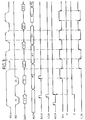
- FIG. 1 represents a memory circuit of which the architecture makes it possible to implement the method of the invention.
- a map memory is organized in rows and columns. All the cells in the same row have the same grid. All cells in the same column have the same drain. The cell sources are brought together at a node common circuit. Access to a cell is by applying a voltage UG on the row connected to the grid of this cell, a voltage UD on the column connected to the drain of this cell and a US voltage on the common node of the sources.
- Reading a Flash EPROM cell is thus obtained by applying a voltage of grid UG of the order of 5 volts (VCC), on the column, a drain voltage UD of the order of 1 volt and on the common node of the sources of the memory plane, a US voltage equal to zero volts (VSS). The contents of the cell are read on the column.
- the programming of an EPROM flash cell is obtained by applying a voltage of grid UG equal to approximately 12 volts (VPP), on the column a drain voltage UD of the order of 6 volts, and at common node of the sources of the memory plane, a voltage of US source equal to zero volts (VSS).
- VPP 12 volts
- UD drain voltage
- US source zero volts
- the erasure is obtained by applying a voltage grid UG equal to the mass VSS, the column being non connected and the US source voltage at approximately 9 volts.
- a verification reading is preferably performed after a write or program operation. This reading is advantageously done at a gate voltage UG higher than in normal reading, of the order of 7 volts.
- External input / output signals D0-D7 arrive on the one hand as input E of a register 1 which delivers the internal data input bus of the circuit marked D-BUS.
- Register 1 also receives the output bus of S-MEM data of the MEM memory plane, to deliver in output S of the register, a data read in memory, under validation signal / OE check.
- This output S is connected to outputs D0-D7.
- the D-BUS data input bus is connected in entry of a data storage register 2 of which the output marked E-MEM is connected to the input circuit of 8th programming associated with circuit 8 of control of bit lines or columns of the memory plane SAME.
- Data storage register 2 receives a clock signal D-CLK which causes, on a pulse, the memorization of a data present on the bus D-BUS data.
- the input circuit 8e notably comprises, in known manner, writing amplifiers (not shown).
- the control door circuit 8 is, for elsewhere, associated with an 8s output circuit comprising read amplifiers and output registers and which delivers the S-MEM output of the memory plane.
- Address signals A0-A15 are transmitted in internal on the A-BUS address bus, connected to the decoder DEC address of the memory plan.
- This decoder includes conventionally a row address DR decoder (or word line), a DC column address decoder (or bit line) and a storage register address 9.
- This register 9 receives as input the address bus A-BUS, and an A-CLK clock signal. An impulse of this signal causes the present address to be memorized on the address bus in register 9 and decoding of this address by the DR and DC decoders.
- the DR decoder receives an input command grid voltage UG which it applies to the row designated by the decoded address, the other rows being maintained for example at ground VSS.
- the DC decoder receives as input a command in drain voltage UD which it applies to the designated columns by the decoded address, the other columns being, for example, not connected.
- the address of a word from the memory map designates a single row and a or more columns.
- the number of designated columns corresponds to the number of data bits of a word memory. In the example where the data is on 8 bits (byte), an address of a memory word designates 1 row and 8 columns, each column being associated with a bit of determined weight of the data word.
- the programming voltage will only be applied on columns whose value of the corresponding bit in the data to be programmed takes the so-called programming value. In one example, if the programmed state of a cell is logic state 1, if the data to be programmed is equal to 55 H (hexadecimal), only the columns associated with the weight bits 0, 2, 4 and 6 will be applied the programming voltage.
- the DC decoder therefore does not directly apply the grid voltage UG on the columns. He applies it to through the data programming circuit 8e and the door circuit 8 for column control.
- the circuit 8e data programming is selected for programming a memory address with a data D stored in the data register 2. It receives this data on the output E-MEM bus of the register 2.
- the door circuit 8 is controlled by programming by the DC decoder to select the columns addressed and by the programming circuit of 8th data to program only the designated columns by data D.
- control register 3 The operation of such a memory is controlled by a control register 3 and sequencing circuits of tasks.
- a first circuit 50 for controlling the voltage of grid UG receives on the one hand, the signal of P-K programming command and in the example shown, the programming check command signal T-K. It switches the voltage on its UG output corresponding to the active input command, voltage that it generates from external voltages.
- the external voltage used by the circuit 50 to generate the voltages VPG and VTG is the high voltage VPP (12 volts).
- VPP the high voltage
- a second circuit 51 for controlling the voltage of drain UD receives the same control signals as input. It generates the corresponding drain voltages of VPD programming (5 volts) and verification VTD programming (1 volt) in the example from supply voltage VCC (5 volts) of the circuit and switches the voltage associated with the level to its output UD active command input.
- a third circuit 52 for controlling the source voltage US from memory plane receives input the same control signals P-K and T-K and, in the case represented from an EPROM flash memory, the VSS voltage of circuit mass. It is this VSS voltage which is switched to the US output in both cases (programming or programming check).
- the write authorization signal / WE is applied in input of a circuit 10 for generating A-CLK clocks and D-CLK.
- the output 150 of this door NOR-OR 15 is connected to an input of a door 16 OR.
- the other input of this door 16 receives the signal from programming mode in uniform field F.
- the output of gate 16 OR delivers the clock signal A-CLK.
- the address present in the memory decoder is then the address present at the same time on the address bus ABUSE.
- the clock signal I-CLK is normally a copy of the data storage clock signal D-CLK, except in programming (normal or uniform) where it must be inhibited.
- a signal generation circuit 20 clock I-CLK thus includes a NOR gate 21 which receives as input the programming mode signals normal P and uniform F and whose output 210 is connected as an input on a door 22 AND. This door 22 receives on another input the clock signal D-CLK. Gate 22 delivers the clock signal at output 220 I-CLK.
- a circuit 30 for generating the control of P-K programming comprises in known manner a first flip-flop 31 which receives the signal P from normal programming mode, and the memory clock D-CLK data. It delivers on its exit 310 the control register 3 reset signal CLR and the normal programming control signal P-KP.
- the circuit 30 for generating the programming command signal has a second flip-flop 32.
- This flip-flop receives as input uniform programming mode F signal and signal D-CLK clock. Its output 320 is connected to a entrance of a door 33 AND, from which the other entrance receives the output validation signal / OE.
- This door 33 AND delivers on its output 330 the command signal of uniform programming P-KF.
- the outputs 310 of the first flip-flop 31 and 330 of door 33 AND are connected to the input of a door 34 OR whose output 340 delivers the P-K command signal memory programming.
- a circuit 40 for generating the control of verification after programming T-K has a door 41 OR receiving as input the verification mode signal normal programming TP and mode signal TF uniform programming check. He delivers as output the control command signal of T-K programming which controls the application of read voltages in VTG and VTD verification, respectively of the order of 7 volts and 1 volt for a EPROM flash memory. (In case the verification is done at normal read voltages the voltage of grid UG is then 5 volts).
- the programming check mode signal uniform TF is issued by the exit of a door 42 AND which receives as input the programming mode signal uniform F issued by the control register 3 and the reverse validation signal OE.
- T-K programming command is therefore active on the active level of the validation signal / OE, level which allows the S-MEM output of the ST data read in memory on data signals D0-D7.
- the signal programming command T-K is the copy of the signal TP mode. In general, we then wait for a few microseconds to activate the validation signal / OE in output, while reading is in progress.
- the order register 3 activates the mode signal P at 1.
- data D0 is stored in the data register 2, and an address M0 is memorized in register 9 of the decoder.
- the clock signal I-CLK is inactive (circuit 20).
- the scale 31 delivers then an active level equal to 1 on its output.
- This level active on the one hand controls the start of programming: P-KP and P-K signals go to 1, which controls the application of the programming voltages on the memory address M0.
- this active level commands the CLR reset of command register 3: the P mode signal returns to zero.
- a third cycle (3) writing generates a new D-CLK pulse. But the A-CLK pulse is inhibited (doors 6, 15) because the normal programming command PK-P is active. That keeps the address programmed in the decoder.
- the flip-flop 31 delivers a level 0 at output and therefore the signal of programming command P-K returns to zero: programming of the address M0 with the data D0 is completed.
- An address programming sequence thus includes 3 writing cycles (1), (2) and (3). The programming time is controlled by both last write cycles.
- the IT verification instruction normal programming is written in the register 3 during the third writing cycle (3).
- This third cycle indeed generates an I-CLK pulse, since in the second write cycle, the mode signal P has been reset (circuits 20 and 30).
- This command is a reading of the memory address which has just been programmed, and which is still present in the third cycle write (3) in register 9 of the decoder, the pulse A-CLK being inhibited in the third write cycle through door 15.
- the timing diagram of the programming sequence uniform is shown in Figure 3.
- the command register 3 activates the mode signal F to 1.
- This mode signal F then forces the A-CLK clock signal at the high level, which makes the transparent address bus for the DEC decoder of the memory.
- the I-CLK clock signal is forced to low level inactive.
- data D is stored in data register 2 and an M0 address presented and maintained on the bus A-BUS address is decoded by the DEC decoder.
- the flip-flop 32 delivers an active output level.
- the exit from door 33 controls a high level on the P-K programming command signal, which commands application of programming voltages to the address M0.
- the change to the active low level of the validation signal / OE results in the zeroing of the P-K command (door 33): programming is stopped.
- a new address M1 can be positioned and maintained on the bus address.
- Switching to the inactive signal level validation / OE will order the programming of this address M1 with the data D always stored in the data register 2.
- the programming time is controlled by the duration between two active pulses of the signal validation / OE.
- Normal and field programming sequences uniform described with verification after programming correspond to the preferred case of programming by successive approach.
- the programming time is relatively short (around 10 microseconds), and it is possible to reprogram the same address, if the ST data read after programming it's not enough.
- This well-known method of programming allows you to best approach a threshold of determined conduction voltage of the programmed cells. This increases reliability (cells less stressed) and the speed of programming.
- the uniform field programming in a first cycle writing.
- the method of the invention makes it possible to eliminate the instruction code write cycles, except the first and the write cycles of the data to be programmed, except the first, when the same data must be programmed in several addresses. This results in one particularly significant time savings, especially for the programming of a large part of the memory.
Landscapes
- Read Only Memory (AREA)
Claims (9)
- Verfahren zur Programmierung einer Dateneinheit D in einem elektrisch programmierbaren Speicher in einem integrierten Schaltkreis mit einem Eingangs-/Ausgangs-Datenbus (D-BUS/S-MEM), einem Adreßbus (A-BUS), einem Befehlsregister (3) für Moden der Abfolge von Befehlen und eines Freigabesignals (/OE), wobei dieses Signal den Datenausgangsbus (S-MEM) in einem aktiven Zustand freigibt, dadurch gekennzeichnet, daß beim Empfang eines Befehls zur uniformen Programmierung (IF) durch das Steuerregister (3) dieses ein Signal für den Mode des Ablaufs der uniformen Programmierung (IF) abschickt, damit das Freigabesignal (/OE) die Programmierung der Dateneinheit D bei einer Speicheradresse steuert, die auf dem Adreßbus in dem inaktiven Zustand (/OE=1) anliegt, und die Unterbrechung der Programmierung in dem aktiven Zustand (/OE=0) steuert.
- Verfahren der Programmierung nach Anspruch 1, dadurch gekennzeichnet, daß eine erste zu programmierende Adresse (M0) auf den Adreßbus (A-BUS) und die Dateneinheit D in ein Datenregister (2) geschrieben wird, um diese erste Adresse (M0) zu programmieren, wobei das Freigabesignal (/OE) sich im inaktiven Zustand (/OE=1) befindet, der Übergang in den aktiven Zustand des Freigabesignals (/OE) die Programmierung der ersten Adresse (M0) unterbricht.
- Verfahren der Programmierung nach Anspruch 2, dadurch gekennzeichnet, daß eine neue zu programmierende Adresse (M1) auf den Adreßbus (A-BUS) während des aktiven Pegels des Freigabesignals (/OE=0) geschrieben wird und programmiert wird mit der Dateneinheit D auf dem inaktiven Pegel nach dem Freigabesignal (/OE).
- Verfahren der Programmierung nach Anspruch 2 oder 3, dadurch gekennzeichnet, daß die auf einen inaktiven Pegel programmierte Adresse auf dem aktiven Pegel nach dem Freigabesignal (/OE) gelesen wird.
- Verfahren der Programmierung nach Anspruch 4, dadurch gekennzeichnet, daß eine Adresse auf den Adreßbus auf einem aktiven Pegel des Freigabesignals (/OE) nach einem Lesen während des aktiven Pegels der programmierten Adresse bei dem vorangehenden inaktiven Pegel geschrieben wird.
- Elektrisch programmierbarer Speicher in einem integrierten Schaltkreis mit einem Adreßbus, einem Eingangs-/Ausgangs-Datenbus (D-BUS/S-MEM) und einem Befehlsregister (3) für den Mode der Abfolge eines Befehls auch ein Freigabesignal (/OE) empfangend, wobei dieses Signal den Datenausgangsbus (S-MEM) auf einem aktiven Zustand freigibt, und ein Schreibfreigabesignal (/WE) zum Erzeugen eines Taktsignals (D-CLK) zum Abspeichern von Daten in einem Datenregister (2), einen Taktgeber (A-CLK) zum Abspeichern der Adresse in einem Dekoder (DEC) des Speichers und einen Taktgeber (I-CLK) zum Abspeichern von Befehlen in dem Befehlsregister (3), dadurch gekennzeichnet, daß er außerdem Vorrichtungen (32, 33) zum Ausgeben eines Signals zum Steuern der uniformen Programmierung (P-KF), die am Eingang ein Modesignal für die uniforme Programmierung (F) empfangen, einen Taktgeber (D-CLK) zum Abspeichern von Daten und des Freigabesignals (/OE) und zum Ausgeben am Ausgang (330) eines aktiven Pegels des Signals zum Steuern der uniformen Programmierung (P-KF=1) auf einem inaktiven Pegel des Freigabesignals (/OE=0) und eines inaktiven Pegels des Signals zur Steuerung der uniformen Programmierung (P-KF=0) auf einem aktiven Pegel des Freigabesignals (/OE=1) umfaßt, wobei das Modesignal der uniformen Programmierung (F) ausgegeben wird durch das Befehlsregister (3).
- Speicher nach Anspruch 6, dadurch gekennzeichnet, daß er außerdem Vorrichtungen (16) umfaßt, um einen durchgehenden Pegel dem Taktgeber zum Abspeichern von Adressen (A-CLK) aufzuzwingen, wobei diese Vorrichtungen gesteuert werden durch das Modesignal der uniformen Programmierung (F).
- Speicher nach Anspruch 6 oder 7, dadurch gekennzeichnet, daß er Vorrichtungen (40) umfaßt, um ein Lesesteuersignal (T-K) auszugeben, wobei diese Vorrichtungen am Eingang das Modesignal der uniformen Programmierung (F) und das Freigabesignal (/OE) empfangen, wobei sie ein Lesesteuersignal (T-K) ausgeben, das aktiv auf dem aktiven Pegel des Freigabesignals (/OE) ist.
- Speicher nach einem der Ansprüche 6 bis 8, dadurch gekennzeichnet, daß die Vorrichtungen zum Ausgeben eines Befehls zur uniformen Programmierung (P-KP) eine Kippstufe (32) beinhalten, die am Eingang des Modesignals der uniformen Programmierung (F), am Taktgeber den Taktgeber (D-CLK) zum Abspeichern von Daten empfängt und ein Ausgangssignal (320) ausgibt, das mit dem Eingang eines UND-Gatters (33) verbunden ist, wobei der andere Eingang des UND-Gatters das Freigabesignal (/OE) empfängt, wobei der Ausgang des UND-Gatters (33) das Signal zur Steuerung der uniformen Programmierung (P-KF) ausgibt.
Applications Claiming Priority (2)
| Application Number | Priority Date | Filing Date | Title |
|---|---|---|---|
| FR9215993 | 1992-12-31 | ||
| FR9215993A FR2700056B1 (fr) | 1992-12-31 | 1992-12-31 | Procédé de programmation en champ uniforme d'une mémoire électriquement programmable et mémoire mettant en Óoeuvre le procédé. |
Publications (2)
| Publication Number | Publication Date |
|---|---|
| EP0606796A1 EP0606796A1 (de) | 1994-07-20 |
| EP0606796B1 true EP0606796B1 (de) | 1998-03-04 |
Family
ID=9437346
Family Applications (1)
| Application Number | Title | Priority Date | Filing Date |
|---|---|---|---|
| EP93403063A Expired - Lifetime EP0606796B1 (de) | 1992-12-31 | 1993-12-16 | Verfahren zur uniformen Programmierung eines elektrisch programmierbaren Speichers und Speicher zur Durchführung des Verfahrens |
Country Status (5)
| Country | Link |
|---|---|
| US (1) | US5457651A (de) |
| EP (1) | EP0606796B1 (de) |
| JP (1) | JPH06282995A (de) |
| DE (1) | DE69317250T2 (de) |
| FR (1) | FR2700056B1 (de) |
Families Citing this family (7)
| Publication number | Priority date | Publication date | Assignee | Title |
|---|---|---|---|---|
| JPH07192481A (ja) * | 1993-12-27 | 1995-07-28 | Mitsubishi Electric Corp | 半導体記憶装置 |
| US5650734A (en) * | 1995-12-11 | 1997-07-22 | Altera Corporation | Programming programmable transistor devices using state machines |
| US6157210A (en) * | 1997-10-16 | 2000-12-05 | Altera Corporation | Programmable logic device with circuitry for observing programmable logic circuit signals and for preloading programmable logic circuits |
| US6507881B1 (en) * | 1999-06-10 | 2003-01-14 | Mediatek Inc. | Method and system for programming a peripheral flash memory via an IDE bus |
| DE102004031700B4 (de) | 2004-06-30 | 2010-02-18 | Airbus Deutschland Gmbh | Flugzeug mit Informationsanzeigesystem |
| TW200636471A (en) * | 2005-04-01 | 2006-10-16 | Mediatek Inc | Method of parallel programmable memory and the system thereof |
| CN114267396B (zh) * | 2021-11-19 | 2025-08-05 | 芯天下技术股份有限公司 | 闪存芯片编程方法、装置、系统、电子设备及存储介质 |
Family Cites Families (2)
| Publication number | Priority date | Publication date | Assignee | Title |
|---|---|---|---|---|
| US5053990A (en) * | 1988-02-17 | 1991-10-01 | Intel Corporation | Program/erase selection for flash memory |
| JPH04206094A (ja) * | 1990-11-30 | 1992-07-28 | Mitsubishi Electric Corp | 不揮発性半導体記憶装置 |
-
1992
- 1992-12-31 FR FR9215993A patent/FR2700056B1/fr not_active Expired - Fee Related
-
1993
- 1993-12-16 DE DE69317250T patent/DE69317250T2/de not_active Expired - Fee Related
- 1993-12-16 EP EP93403063A patent/EP0606796B1/de not_active Expired - Lifetime
- 1993-12-29 JP JP5352617A patent/JPH06282995A/ja not_active Withdrawn
-
1994
- 1994-01-03 US US08/177,116 patent/US5457651A/en not_active Expired - Lifetime
Also Published As
| Publication number | Publication date |
|---|---|
| FR2700056A1 (fr) | 1994-07-01 |
| EP0606796A1 (de) | 1994-07-20 |
| DE69317250T2 (de) | 1998-06-25 |
| US5457651A (en) | 1995-10-10 |
| DE69317250D1 (de) | 1998-04-09 |
| JPH06282995A (ja) | 1994-10-07 |
| FR2700056B1 (fr) | 1995-02-10 |
Similar Documents
| Publication | Publication Date | Title |
|---|---|---|
| EP0791933B1 (de) | Elektrisch modifizierbarer nichtflüchtiger Mehrpegelspeicher mit autonomer Auffrischung | |
| EP0674264B1 (de) | Schaltung zum Wählen von Redundanzspeicherbauelementen und diese enthaltende FLASH EEPROM | |
| EP0618591B1 (de) | Integrierte Schaltung für Speicherkarte und Verfahren zum Abzählen der Einheiten in einer Speicherkarte | |
| FR2728380A1 (fr) | Procede d'ecriture de donnees dans une memoire et memoire electriquement programmable correspondante | |
| FR2627315A1 (fr) | Procede de preconditionnement, effacement et/ou programmation d'un composant de memoire eeprom | |
| EP0318363A1 (de) | Verfahren zum Testen von Zellen von elektrisch programmierbaren Speichern und entsprechende integrierte Schaltung | |
| FR2778012A1 (fr) | Dispositif et procede de lecture de cellules de memoire eeprom | |
| EP0567356A1 (de) | Vorrichtung und Verfahren zum Löschen von Sektoren eines Flash-EPROM-Speichers | |
| EP1111621A1 (de) | Seitenprogrammierbar Flash-Speicher | |
| FR2633749A1 (fr) | Systeme microprocesseur avec une memoire morte programmable effacable electriquement ayant une fonction de prevention des erreurs d'ecriture et circuit de memoire | |
| FR2711834A1 (fr) | Circuit programmable de mémoire de codes pour mémoire flash. | |
| EP0606796B1 (de) | Verfahren zur uniformen Programmierung eines elektrisch programmierbaren Speichers und Speicher zur Durchführung des Verfahrens | |
| EP1573541A2 (de) | Verfahren um daten mit fehlerkorrektur zu speichern | |
| FR2771839A1 (fr) | Memoire non volatile programmable et effacable electriquement | |
| FR2801419A1 (fr) | Procede et dispositif de lecture pour memoire en circuit integre | |
| EP1630820B1 (de) | Speicherzellenprogrammierverfahren mit Detektion von Transkonduktanzdegradierung | |
| EP0703584B1 (de) | Adressen-Dekodierverfahren für einen integrierten Speicher und Speicherschaltung zur Anwendung eines solchen Verfahrens | |
| EP1374249A1 (de) | Vorrichtung und verfahren zur teilweisen lesebeschützung eines nichtflüchtigen speichers | |
| EP0875899B1 (de) | Anordnung von zwei Speichern auf der selben monolitischen integrierten Schaltung | |
| EP0678875B1 (de) | Verfahren und Schaltungen zur Löschung eines Speichers | |
| EP1486987A1 (de) | Flash-Speicher mit Mitteln zum Steuern und Auffrischen von Speicherzellen im gelöschten Zustand | |
| FR2851843A1 (fr) | Memoire flash comprenant un algorithme de verification d'effacement integre dans un algorithme de programmation | |
| EP1158408B1 (de) | EEPROM Speicher mit Fehlerkorrekturvorrichtung | |
| EP1085520B1 (de) | Seitenprogrammiermodus für EEPROM und zugehörige Schaltung | |
| FR2719939A1 (fr) | Mémoire non volatile modifiable électriquement à interface de commande. |
Legal Events
| Date | Code | Title | Description |
|---|---|---|---|
| PUAI | Public reference made under article 153(3) epc to a published international application that has entered the european phase |
Free format text: ORIGINAL CODE: 0009012 |
|
| 17P | Request for examination filed |
Effective date: 19940418 |
|
| AK | Designated contracting states |
Kind code of ref document: A1 Designated state(s): DE FR GB IT |
|
| GRAG | Despatch of communication of intention to grant |
Free format text: ORIGINAL CODE: EPIDOS AGRA |
|
| 17Q | First examination report despatched |
Effective date: 19970325 |
|
| GRAH | Despatch of communication of intention to grant a patent |
Free format text: ORIGINAL CODE: EPIDOS IGRA |
|
| GRAH | Despatch of communication of intention to grant a patent |
Free format text: ORIGINAL CODE: EPIDOS IGRA |
|
| GRAA | (expected) grant |
Free format text: ORIGINAL CODE: 0009210 |
|
| ITF | It: translation for a ep patent filed | ||
| AK | Designated contracting states |
Kind code of ref document: B1 Designated state(s): DE FR GB IT |
|
| GBT | Gb: translation of ep patent filed (gb section 77(6)(a)/1977) |
Effective date: 19980305 |
|
| REF | Corresponds to: |
Ref document number: 69317250 Country of ref document: DE Date of ref document: 19980409 |
|
| PLBE | No opposition filed within time limit |
Free format text: ORIGINAL CODE: 0009261 |
|
| STAA | Information on the status of an ep patent application or granted ep patent |
Free format text: STATUS: NO OPPOSITION FILED WITHIN TIME LIMIT |
|
| RAP4 | Party data changed (patent owner data changed or rights of a patent transferred) |
Owner name: STMICROELECTRONICS S.A. |
|
| 26N | No opposition filed | ||
| REG | Reference to a national code |
Ref country code: GB Ref legal event code: IF02 |
|
| PGFP | Annual fee paid to national office [announced via postgrant information from national office to epo] |
Ref country code: DE Payment date: 20020109 Year of fee payment: 9 |
|
| PG25 | Lapsed in a contracting state [announced via postgrant information from national office to epo] |
Ref country code: DE Free format text: LAPSE BECAUSE OF NON-PAYMENT OF DUE FEES Effective date: 20030701 |
|
| PGFP | Annual fee paid to national office [announced via postgrant information from national office to epo] |
Ref country code: FR Payment date: 20041208 Year of fee payment: 12 |
|
| PGFP | Annual fee paid to national office [announced via postgrant information from national office to epo] |
Ref country code: GB Payment date: 20041215 Year of fee payment: 12 |
|
| PG25 | Lapsed in a contracting state [announced via postgrant information from national office to epo] |
Ref country code: IT Free format text: LAPSE BECAUSE OF NON-PAYMENT OF DUE FEES Effective date: 20051216 Ref country code: GB Free format text: LAPSE BECAUSE OF NON-PAYMENT OF DUE FEES Effective date: 20051216 |
|
| GBPC | Gb: european patent ceased through non-payment of renewal fee |
Effective date: 20051216 |
|
| PG25 | Lapsed in a contracting state [announced via postgrant information from national office to epo] |
Ref country code: FR Free format text: LAPSE BECAUSE OF NON-PAYMENT OF DUE FEES Effective date: 20060831 |
|
| REG | Reference to a national code |
Ref country code: FR Ref legal event code: ST Effective date: 20060831 |