EP0607940A2 - Verfahren zum Schützen der Oberfläche eines halbleitenden Substrats während des Schleifens - Google Patents
Verfahren zum Schützen der Oberfläche eines halbleitenden Substrats während des Schleifens Download PDFInfo
- Publication number
- EP0607940A2 EP0607940A2 EP94100715A EP94100715A EP0607940A2 EP 0607940 A2 EP0607940 A2 EP 0607940A2 EP 94100715 A EP94100715 A EP 94100715A EP 94100715 A EP94100715 A EP 94100715A EP 0607940 A2 EP0607940 A2 EP 0607940A2
- Authority
- EP
- European Patent Office
- Prior art keywords
- wafer
- semiconductor wafer
- back surface
- layer
- polishing
- Prior art date
- Legal status (The legal status is an assumption and is not a legal conclusion. Google has not performed a legal analysis and makes no representation as to the accuracy of the status listed.)
- Granted
Links
Images

Classifications
-
- H—ELECTRICITY
- H10—SEMICONDUCTOR DEVICES; ELECTRIC SOLID-STATE DEVICES NOT OTHERWISE PROVIDED FOR
- H10P—GENERIC PROCESSES OR APPARATUS FOR THE MANUFACTURE OR TREATMENT OF DEVICES COVERED BY CLASS H10
- H10P90/00—Preparation of wafers not covered by a single main group of this subclass, e.g. wafer reinforcement
- H10P90/12—Preparing bulk and homogeneous wafers
-
- B—PERFORMING OPERATIONS; TRANSPORTING
- B24—GRINDING; POLISHING
- B24B—MACHINES, DEVICES, OR PROCESSES FOR GRINDING OR POLISHING; DRESSING OR CONDITIONING OF ABRADING SURFACES; FEEDING OF GRINDING, POLISHING, OR LAPPING AGENTS
- B24B9/00—Machines or devices designed for grinding edges or bevels on work or for removing burrs; Accessories therefor
- B24B9/02—Machines or devices designed for grinding edges or bevels on work or for removing burrs; Accessories therefor characterised by a special design with respect to properties of materials specific to articles to be ground
- B24B9/06—Machines or devices designed for grinding edges or bevels on work or for removing burrs; Accessories therefor characterised by a special design with respect to properties of materials specific to articles to be ground of non-metallic inorganic material, e.g. stone, ceramics, porcelain
- B24B9/065—Machines or devices designed for grinding edges or bevels on work or for removing burrs; Accessories therefor characterised by a special design with respect to properties of materials specific to articles to be ground of non-metallic inorganic material, e.g. stone, ceramics, porcelain of thin, brittle parts, e.g. semiconductors, wafers
-
- Y—GENERAL TAGGING OF NEW TECHNOLOGICAL DEVELOPMENTS; GENERAL TAGGING OF CROSS-SECTIONAL TECHNOLOGIES SPANNING OVER SEVERAL SECTIONS OF THE IPC; TECHNICAL SUBJECTS COVERED BY FORMER USPC CROSS-REFERENCE ART COLLECTIONS [XRACs] AND DIGESTS
- Y10—TECHNICAL SUBJECTS COVERED BY FORMER USPC
- Y10S—TECHNICAL SUBJECTS COVERED BY FORMER USPC CROSS-REFERENCE ART COLLECTIONS [XRACs] AND DIGESTS
- Y10S438/00—Semiconductor device manufacturing: process
- Y10S438/959—Mechanical polishing of wafer
Definitions
- This invention relates to semiconductor wafers, and more particularly to a method of backside protection during edge and wafer surface polishing and to methods of mounting during polishing.
- silicon and abrasive particles adhere to the surfaces of the wafer and are difficult to remove.
- Prior art methods have applied films such as photoresist or wax to protect on the back of the wafer. These methods have disadvantages in that materials, equipment and labor are expensive to apply and remove the films. In later processing, the wafer cannot be polished sufficiently flat with the layer in place, and the methods do not protect against "slurry rings". The abrasive edge polish process sometimes lifts a portion of the film away from the wafer, allowing etching under the film in later processing. Wax or photoresist protection involves the extra steps of application and removal.
- Another process used in prior art methods of particle removal is to etch the water with an acid or caustic solution after abrasive edge polishing. This has the disadvantage of removing extrinsic gettering sites (backside damage).
- Template mounting involves the mounting of a template assembly, composed of a poromeric backing material which contracts the backside of the wafer, and a fibreglass/urethane retainer which surrounds the outer diameter of the wafer.
- the assembly is mounted on a polishing block.
- the poromeric backing film compresses non-uniformly during the polishing process, and high quality flatness and taper control can not be achieved. The film also increases greatly the cost of templates and reduces productivity.
- backside wax mounting a layer of wax approximately 4 mils in thickness is deposited on the backside of the wafer, then the wafer is mounted onto a polishing block. Following the polish process, the wafer is demounted from the block and the wax is stripped from the wafer.
- problems with the wax mounting process are: (1) the uniformity of the wax layer is critical to achieving high quality flatness; (2) the wax residues contribute to high particles on the wafer; and (3) particles which are entrapped in the wax layer cause high points, or "dimples" in the polished wafer surface; and there is a yield loss associated with the demounting and the other steps.
- the invention is to a method for protecting the backside of a semiconductor wafer during polishing.
- the method solves the problems of particle adherence, backside etching at mirror edge polish, staining of the back surface, the need for a poromeric backing film in template polishing and backside scratches from mounting on polish blocks, and back reference flatness achievement without wax mounting.
- the protection to the backside of the semiconductor wafer is accomplished by applying a layer of material to the backside of the semiconductor wafer that is known to protect against particles, scratches, and etching by mild caustic solutions.
- the layer remains in place during all three processes, edge pre-polish, mirror edge polish, and wafer polish, or any combination thereof.
- the layer is an oxide or nitride layer such as deposited by a CUD or plasma reactor.
- One layer used is an oxide layer of Silox. Any portion of the layer that wraps around the rounded edge can be abraded away by the abrasive wheel pre-polish without lifting the layer.
- the layer protects during the chem-mechanical mirror edge polish step without introducing a high friction or self-adhesive layer.
- Existing clean up process after polishing includes a hydrofluoric acid treatment, which removes the layer without any added chemical step.
- the oxide or nitride layer protects the back surface when the wafer is mounted directly to a polishing block, and held in position by using only the fiberglass template portion of the template assembly.
- the back reference for the polished wafer is the polishing block.
- the protective layer also permits wafers to be single sided polished on a double-side polishing machine, which produces the highest quality of flatness currently available.
- Another advantage of the invention is that it makes easier the application of the mirror edge polish process (e.g. US. Patent 5,128,281) and its advantages.
- One such is to avoid sources of misfit dislocation nucleations during epitaxial deposition.
- Figure 1 is a simplified illustration of a edge polishing process and, apparatus.
- a plurality of semiconductor wafers IQ are held together by clamping plates 12 which rotate around shafts 13 and 14.
- the wafers have spacers 11 sandwiched between the wafers.
- the stack of wafers is rotated, for example, in the direction of arrow 23.
- roller 15 which has a pad 15a on its surface.
- the wafer edges are in contact with pad 15a.
- Roller 15 is rotated by shafts 17 and 18, for example, in the direction of arrow 24.
- a chemomechanical slurry mixture is applied by dispenser 19 through holes 20. Slurry is introduced into dispenser at its end, as shown by arrow 22.
- Roller pad 15a has a series of grooves 16 that extend into the surface of the pad and partially around the outer circumference of pad 15a. Grooves 16 are spaced such that an edge of a wafer enters a groove as the wafers and roller are rotated. The edge of a wafer is in a groove only during a part of a complete rotation since each groove does not extend completely around the outer circumference of pad 15a.
- roller 15 As roller 15 rotates, the edges of the semiconductor wafers are moved into and out of grooves 16 alternately polishing the edge and the sides of the edge to provide a polished tapered edge on the semiconductor wafer.
- Figure 2 shows apart of the mounted wafers, for example, two wafers mounted between spacers II, and the exposed back surface 30 of the wafers that is not protected during polishing. If the exposed back surface is not protected, the surface, including backside damage done during a previous step could be scratched or etched by slurry residue. The front surface need not be protected because any slight etching will be removed during the polish operation.
- Figure 3 shows a mounted semiconductor wafer 10 with a layer 32 of silicon oxide or silicon nitride on its back surface side.
- the protection to the back surface of the semiconductor wafer is accomplished by applying a layer of material to the backside layer 32 of the semiconductor wafer that is known to protect against particles, scratches, and etching by mild caustic solutions.
- the backside layer 32 remains in place, and the layer edge 32a is not lifted during edge pre-polish, mirror edge polish, and wafer polish.
- the layer is of an oxide or nitride layer such as deposited by a CUD or plasma reactor.
- One layer used, for example, is a oxide layer of Silox. Any portion of a layer that wraps around the round edge can be abraded away on the edge by the abrasive wheel pre-polish without lifting the layer.
- the layer protects the wafer back surface during the chem-mechanical mirror edge polish step without introducing a high friction or self-adhesive layer.
- the existing clean up process after polishing includes a hydrofluoric acid treatment, which removes the back surface layer without any added chemical step.
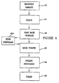
- Figure 4 illustrates basic steps in wafer preparation.
- the backside of the wafer is submitted to an abrasive action to cause backside damage to the wafer.
- Such a process may include "sand blasting" with abrasive particles.
- the wafer is cleaned to remove particles created during backside damage.
- the back surface of the wafer is coated with the coating material as shown in Figure 3.
- Coated wafers are mounted as illustrated in Figure 1 and submitted to edge polishing (step 43), however, the coating layer 32 ( Figure 3) protects the back surface of the wafer, and only the coating at the edges of the wafer are removed. The remaining portion of the layer is not lifted or otherwise removed from the surface of the wafer.
- a pre-polish step 43a may also be included.
- the edge polished wafers are then mounted in a surface polisher, step 44, to provide a chemomechanical, damage-free polish to the front side of the wafer.
- the wafer Normally in polishing the wafer, the wafer would be wax mounted or placed in a template with the wafer position in the template with the backside on a pad to protect the backside from the mounting surface of the polishing machine, However, because of the protective coating 32 on the back side of the wafer, the wafer may be mounted directly on the mounting surface of the polishing machine.
- the mounting surface usually an aluminium or ceramic material will not scratch the surface of the wafer because of layer 32 thereon.
- the wafer After the front side has been polished, the wafer undergoes a cleaning process to remove slurry residue and particles If the wafer has a back surface coating of silicon oxide, it will be removed also because hydrofluoric acid is used. If the wafer has some other back surface coating, some other chemical will be used to remove it.
Landscapes
- Engineering & Computer Science (AREA)
- Chemical & Material Sciences (AREA)
- Ceramic Engineering (AREA)
- Inorganic Chemistry (AREA)
- Mechanical Engineering (AREA)
- Mechanical Treatment Of Semiconductor (AREA)
Applications Claiming Priority (2)
| Application Number | Priority Date | Filing Date | Title |
|---|---|---|---|
| US5713 | 1993-01-19 | ||
| US08/005,713 US5424224A (en) | 1993-01-19 | 1993-01-19 | Method of surface protection of a semiconductor wafer during polishing |
Publications (3)
| Publication Number | Publication Date |
|---|---|
| EP0607940A2 true EP0607940A2 (de) | 1994-07-27 |
| EP0607940A3 EP0607940A3 (de) | 1996-12-27 |
| EP0607940B1 EP0607940B1 (de) | 2001-11-21 |
Family
ID=21717325
Family Applications (1)
| Application Number | Title | Priority Date | Filing Date |
|---|---|---|---|
| EP94100715A Expired - Lifetime EP0607940B1 (de) | 1993-01-19 | 1994-01-19 | Verfahren zum Schützen der Oberfläche eines halbleitenden Substrats während des Schleifens |
Country Status (4)
| Country | Link |
|---|---|
| US (1) | US5424224A (de) |
| EP (1) | EP0607940B1 (de) |
| JP (1) | JPH06349796A (de) |
| DE (1) | DE69429122T2 (de) |
Cited By (4)
| Publication number | Priority date | Publication date | Assignee | Title |
|---|---|---|---|---|
| EP0813931A1 (de) * | 1996-05-22 | 1997-12-29 | Shin-Etsu Handotai Company Limited | Verfahren zur Herstellung von Halbleiterscheiben |
| EP0826459A1 (de) * | 1996-08-27 | 1998-03-04 | Shin-Etsu Handotai Company Limited | Verfahren und Vorrichtung zum Abfasen von Halbleiterscheiben mit losem Schleifkorn |
| US6051498A (en) * | 1997-02-06 | 2000-04-18 | Wacker Siltronic Gesellschaft Fur Halbleitermaterialien Ag | Method for manufacturing a semiconductor wafer which is coated on one side and provided with a finish |
| EP0877418A3 (de) * | 1997-05-09 | 2000-08-09 | Speedfam Co., Ltd. | Verfahren und Vorrichtung zum Abfasen |
Families Citing this family (22)
| Publication number | Priority date | Publication date | Assignee | Title |
|---|---|---|---|---|
| JP2719113B2 (ja) * | 1994-05-24 | 1998-02-25 | 信越半導体株式会社 | 単結晶シリコンウェーハの歪付け方法 |
| US5958794A (en) * | 1995-09-22 | 1999-09-28 | Minnesota Mining And Manufacturing Company | Method of modifying an exposed surface of a semiconductor wafer |
| JPH09270400A (ja) * | 1996-01-31 | 1997-10-14 | Shin Etsu Handotai Co Ltd | 半導体ウェーハの製造方法 |
| US5780204A (en) * | 1997-02-03 | 1998-07-14 | Advanced Micro Devices, Inc. | Backside wafer polishing for improved photolithography |
| US8092707B2 (en) | 1997-04-30 | 2012-01-10 | 3M Innovative Properties Company | Compositions and methods for modifying a surface suited for semiconductor fabrication |
| US6194317B1 (en) | 1998-04-30 | 2001-02-27 | 3M Innovative Properties Company | Method of planarizing the upper surface of a semiconductor wafer |
| US6080042A (en) * | 1997-10-31 | 2000-06-27 | Virginia Semiconductor, Inc. | Flatness and throughput of single side polishing of wafers |
| US6023094A (en) | 1998-01-14 | 2000-02-08 | National Semiconductor Corporation | Semiconductor wafer having a bottom surface protective coating |
| DE19915078A1 (de) | 1999-04-01 | 2000-10-12 | Siemens Ag | Verfahren zur Prozessierung einer monokristallinen Halbleiterscheibe und teilweise prozessierte Halbleiterscheibe |
| US6245677B1 (en) * | 1999-07-28 | 2001-06-12 | Noor Haq | Backside chemical etching and polishing |
| US6376335B1 (en) | 2000-02-17 | 2002-04-23 | Memc Electronic Materials, Inc. | Semiconductor wafer manufacturing process |
| US6622334B1 (en) | 2000-03-29 | 2003-09-23 | International Business Machines Corporation | Wafer edge cleaning utilizing polish pad material |
| US6709981B2 (en) | 2000-08-16 | 2004-03-23 | Memc Electronic Materials, Inc. | Method and apparatus for processing a semiconductor wafer using novel final polishing method |
| US6790125B2 (en) * | 2000-12-11 | 2004-09-14 | International Business Machines Corporation | Backside integrated circuit die surface finishing technique and tool |
| US6852241B2 (en) | 2001-08-14 | 2005-02-08 | Lexmark International, Inc. | Method for making ink jet printheads |
| US7018268B2 (en) * | 2002-04-09 | 2006-03-28 | Strasbaugh | Protection of work piece during surface processing |
| ES2318778T3 (es) * | 2005-06-28 | 2009-05-01 | Eta Sa Manufacture Horlogere Suisse | Pieza de micromecanica reforzada. |
| US7559825B2 (en) * | 2006-12-21 | 2009-07-14 | Memc Electronic Materials, Inc. | Method of polishing a semiconductor wafer |
| JP5795461B2 (ja) * | 2009-08-19 | 2015-10-14 | 株式会社Sumco | エピタキシャルシリコンウェーハの製造方法 |
| CN102044432B (zh) * | 2009-10-13 | 2012-12-05 | 中芯国际集成电路制造(上海)有限公司 | 防止晶圆表面不平及曝光中失焦的方法 |
| KR102674864B1 (ko) * | 2021-10-29 | 2024-06-12 | 오은찬 | 웨이퍼 가공 방법 및 이에 사용되는 웨이퍼 가공 장치 |
| CN115256108B (zh) * | 2022-07-12 | 2023-12-19 | 山东润马光能科技有限公司 | 一种浮动式晶圆边缘打磨方法及装置 |
Family Cites Families (8)
| Publication number | Priority date | Publication date | Assignee | Title |
|---|---|---|---|---|
| US4384919A (en) * | 1978-11-13 | 1983-05-24 | Sperry Corporation | Method of making x-ray masks |
| JPS5958827A (ja) * | 1982-09-28 | 1984-04-04 | Toshiba Corp | 半導体ウエ−ハ、半導体ウエ−ハの製造方法及び半導体ウエ−ハの製造装置 |
| JPS59174514A (ja) * | 1983-03-22 | 1984-10-03 | Hoxan Corp | 多結晶シリコンウエハの製造方法 |
| JPS62132324A (ja) * | 1985-12-04 | 1987-06-15 | Showa Denko Kk | ウエハ−の面取り研削ダメ−ジ層の除去方法および除去用治具 |
| JPS63117427A (ja) * | 1986-11-06 | 1988-05-21 | Mitsubishi Electric Corp | 半導体装置の製造方法 |
| IT1229640B (it) * | 1987-06-29 | 1991-09-04 | S G S Microelettronica S P A O | Processo di conformazione del bordo di fette di materiale semiconduttore e relativa apparecchiatura |
| JPH06103678B2 (ja) * | 1987-11-28 | 1994-12-14 | 株式会社東芝 | 半導体基板の加工方法 |
| US5128281A (en) * | 1991-06-05 | 1992-07-07 | Texas Instruments Incorporated | Method for polishing semiconductor wafer edges |
-
1993
- 1993-01-19 US US08/005,713 patent/US5424224A/en not_active Expired - Lifetime
-
1994
- 1994-01-18 JP JP6003643A patent/JPH06349796A/ja active Pending
- 1994-01-19 DE DE69429122T patent/DE69429122T2/de not_active Expired - Fee Related
- 1994-01-19 EP EP94100715A patent/EP0607940B1/de not_active Expired - Lifetime
Cited By (6)
| Publication number | Priority date | Publication date | Assignee | Title |
|---|---|---|---|---|
| EP0813931A1 (de) * | 1996-05-22 | 1997-12-29 | Shin-Etsu Handotai Company Limited | Verfahren zur Herstellung von Halbleiterscheiben |
| US6080641A (en) * | 1996-05-22 | 2000-06-27 | Shin-Etsu Handotai Co., Ltd. | Method of manufacturing semiconductor wafer |
| EP0826459A1 (de) * | 1996-08-27 | 1998-03-04 | Shin-Etsu Handotai Company Limited | Verfahren und Vorrichtung zum Abfasen von Halbleiterscheiben mit losem Schleifkorn |
| US5944584A (en) * | 1996-08-27 | 1999-08-31 | Shin-Estu Handotai Co., Ltd. | Apparatus and method for chamfering wafer with loose abrasive grains |
| US6051498A (en) * | 1997-02-06 | 2000-04-18 | Wacker Siltronic Gesellschaft Fur Halbleitermaterialien Ag | Method for manufacturing a semiconductor wafer which is coated on one side and provided with a finish |
| EP0877418A3 (de) * | 1997-05-09 | 2000-08-09 | Speedfam Co., Ltd. | Verfahren und Vorrichtung zum Abfasen |
Also Published As
| Publication number | Publication date |
|---|---|
| EP0607940A3 (de) | 1996-12-27 |
| JPH06349796A (ja) | 1994-12-22 |
| US5424224A (en) | 1995-06-13 |
| EP0607940B1 (de) | 2001-11-21 |
| DE69429122T2 (de) | 2002-06-20 |
| DE69429122D1 (de) | 2002-01-03 |
Similar Documents
| Publication | Publication Date | Title |
|---|---|---|
| US5424224A (en) | Method of surface protection of a semiconductor wafer during polishing | |
| US7402520B2 (en) | Edge removal of silicon-on-insulator transfer wafer | |
| EP0537627B1 (de) | Planarisierung eines Halbleitersubstrates | |
| KR100222228B1 (ko) | 웨이퍼 및 기판의 재생방법 및 장치 | |
| EP0687524B1 (de) | Verfahren und Vorrichtung zum Hochglanzpolieren eines Teiles von einem Wafer | |
| JP3247301B2 (ja) | 再生半導体ウェハとその再生方法 | |
| JP3972065B2 (ja) | シリコンダスト除去用ウェーハのグラインディング研磨装置 | |
| US6227944B1 (en) | Method for processing a semiconductor wafer | |
| EP1145296B1 (de) | Herstellungsverfahren einer halbleiterscheibe | |
| KR100690098B1 (ko) | 반도체 웨이퍼의 연마방법 및 반도체 웨이퍼의 연마장치 | |
| EP0990485A2 (de) | Verfahren zur Freigabeverbesserung einer Halbleiterplatte | |
| JP3606432B2 (ja) | 高平坦度ウェーハの製造方法 | |
| US6514423B1 (en) | Method for wafer processing | |
| JPS6381934A (ja) | ウエハおよびその製造方法 | |
| JP3399179B2 (ja) | ウェーハの加工方法 | |
| KR100883511B1 (ko) | 반도체 웨이퍼 연마 방법 및 장치 | |
| JP2001093865A (ja) | 半導体ウェーハの製造方法 | |
| WO1999031723A1 (en) | Method of improving the flatness of polished semiconductor wafers | |
| JP2510038B2 (ja) | 半導体装置の製造方法 | |
| JP4337079B2 (ja) | 半導体ウェーハの面取り面の形成方法 | |
| EP0923122A2 (de) | Chemisch-mechanisches Polierverfahren und System für die Herstellung eines integrierten Schaltkreises | |
| JPH09102477A (ja) | 半導体ウェ−ハおよびその製造方法 | |
| Ghahghahi et al. | Preparation of custom gate array silicon wafers to handle specific wafer size in metallization process | |
| JP2004047742A (ja) | 半導体ウェーハおよびその製造方法 | |
| HK1023535A (en) | Method for enhancing semiconductor wafer release |
Legal Events
| Date | Code | Title | Description |
|---|---|---|---|
| PUAI | Public reference made under article 153(3) epc to a published international application that has entered the european phase |
Free format text: ORIGINAL CODE: 0009012 |
|
| AK | Designated contracting states |
Kind code of ref document: A2 Designated state(s): DE FR GB IT NL |
|
| PUAL | Search report despatched |
Free format text: ORIGINAL CODE: 0009013 |
|
| AK | Designated contracting states |
Kind code of ref document: A3 Designated state(s): DE FR GB IT NL |
|
| 17P | Request for examination filed |
Effective date: 19970915 |
|
| 17Q | First examination report despatched |
Effective date: 19990311 |
|
| GRAG | Despatch of communication of intention to grant |
Free format text: ORIGINAL CODE: EPIDOS AGRA |
|
| GRAG | Despatch of communication of intention to grant |
Free format text: ORIGINAL CODE: EPIDOS AGRA |
|
| GRAH | Despatch of communication of intention to grant a patent |
Free format text: ORIGINAL CODE: EPIDOS IGRA |
|
| GRAH | Despatch of communication of intention to grant a patent |
Free format text: ORIGINAL CODE: EPIDOS IGRA |
|
| ITF | It: translation for a ep patent filed | ||
| GRAA | (expected) grant |
Free format text: ORIGINAL CODE: 0009210 |
|
| AK | Designated contracting states |
Kind code of ref document: B1 Designated state(s): DE FR GB IT NL |
|
| REG | Reference to a national code |
Ref country code: GB Ref legal event code: IF02 |
|
| REF | Corresponds to: |
Ref document number: 69429122 Country of ref document: DE Date of ref document: 20020103 |
|
| ET | Fr: translation filed | ||
| PLBE | No opposition filed within time limit |
Free format text: ORIGINAL CODE: 0009261 |
|
| STAA | Information on the status of an ep patent application or granted ep patent |
Free format text: STATUS: NO OPPOSITION FILED WITHIN TIME LIMIT |
|
| 26N | No opposition filed | ||
| PG25 | Lapsed in a contracting state [announced via postgrant information from national office to epo] |
Ref country code: IT Free format text: LAPSE BECAUSE OF NON-PAYMENT OF DUE FEES;WARNING: LAPSES OF ITALIAN PATENTS WITH EFFECTIVE DATE BEFORE 2007 MAY HAVE OCCURRED AT ANY TIME BEFORE 2007. THE CORRECT EFFECTIVE DATE MAY BE DIFFERENT FROM THE ONE RECORDED. Effective date: 20050119 |
|
| PGFP | Annual fee paid to national office [announced via postgrant information from national office to epo] |
Ref country code: NL Payment date: 20090113 Year of fee payment: 16 Ref country code: DE Payment date: 20090130 Year of fee payment: 16 |
|
| PGFP | Annual fee paid to national office [announced via postgrant information from national office to epo] |
Ref country code: GB Payment date: 20081211 Year of fee payment: 16 |
|
| REG | Reference to a national code |
Ref country code: NL Ref legal event code: V1 Effective date: 20100801 |
|
| GBPC | Gb: european patent ceased through non-payment of renewal fee |
Effective date: 20100119 |
|
| REG | Reference to a national code |
Ref country code: FR Ref legal event code: ST Effective date: 20100930 |
|
| PG25 | Lapsed in a contracting state [announced via postgrant information from national office to epo] |
Ref country code: NL Free format text: LAPSE BECAUSE OF NON-PAYMENT OF DUE FEES Effective date: 20100801 Ref country code: FR Free format text: LAPSE BECAUSE OF NON-PAYMENT OF DUE FEES Effective date: 20100201 |
|
| PG25 | Lapsed in a contracting state [announced via postgrant information from national office to epo] |
Ref country code: DE Free format text: LAPSE BECAUSE OF NON-PAYMENT OF DUE FEES Effective date: 20100803 |
|
| PG25 | Lapsed in a contracting state [announced via postgrant information from national office to epo] |
Ref country code: GB Free format text: LAPSE BECAUSE OF NON-PAYMENT OF DUE FEES Effective date: 20100119 |
|
| PGFP | Annual fee paid to national office [announced via postgrant information from national office to epo] |
Ref country code: FR Payment date: 20090106 Year of fee payment: 16 |