EP0608249B2 - Oberflächenwellenfilter mit einem gefalteten akustischen pfad - Google Patents
Oberflächenwellenfilter mit einem gefalteten akustischen pfad Download PDFInfo
- Publication number
- EP0608249B2 EP0608249B2 EP92918770A EP92918770A EP0608249B2 EP 0608249 B2 EP0608249 B2 EP 0608249B2 EP 92918770 A EP92918770 A EP 92918770A EP 92918770 A EP92918770 A EP 92918770A EP 0608249 B2 EP0608249 B2 EP 0608249B2
- Authority
- EP
- European Patent Office
- Prior art keywords
- channels
- filter according
- central
- equal
- wave filter
- Prior art date
- Legal status (The legal status is an assumption and is not a legal conclusion. Google has not performed a legal analysis and makes no representation as to the accuracy of the status listed.)
- Expired - Lifetime
Links
Images

Classifications
-
- H—ELECTRICITY
- H03—ELECTRONIC CIRCUITRY
- H03H—IMPEDANCE NETWORKS, e.g. RESONANT CIRCUITS; RESONATORS
- H03H9/00—Networks comprising electromechanical or electro-acoustic elements; Electromechanical resonators
- H03H9/0023—Networks for transforming balanced signals into unbalanced signals and vice versa, e.g. baluns, or networks having balanced input and output
- H03H9/0028—Networks for transforming balanced signals into unbalanced signals and vice versa, e.g. baluns, or networks having balanced input and output using surface acoustic wave devices
- H03H9/0047—Networks for transforming balanced signals into unbalanced signals and vice versa, e.g. baluns, or networks having balanced input and output using surface acoustic wave devices having two acoustic tracks
- H03H9/0052—Networks for transforming balanced signals into unbalanced signals and vice versa, e.g. baluns, or networks having balanced input and output using surface acoustic wave devices having two acoustic tracks being electrically cascaded
- H03H9/0057—Networks for transforming balanced signals into unbalanced signals and vice versa, e.g. baluns, or networks having balanced input and output using surface acoustic wave devices having two acoustic tracks being electrically cascaded the balanced terminals being on the same side of the tracks
-
- H—ELECTRICITY
- H03—ELECTRONIC CIRCUITRY
- H03H—IMPEDANCE NETWORKS, e.g. RESONANT CIRCUITS; RESONATORS
- H03H9/00—Networks comprising electromechanical or electro-acoustic elements; Electromechanical resonators
- H03H9/02—Details
- H03H9/02535—Details of surface acoustic wave devices
- H03H9/02637—Details concerning reflective or coupling arrays
- H03H9/02653—Grooves or arrays buried in the substrate
-
- H—ELECTRICITY
- H03—ELECTRONIC CIRCUITRY
- H03H—IMPEDANCE NETWORKS, e.g. RESONANT CIRCUITS; RESONATORS
- H03H9/00—Networks comprising electromechanical or electro-acoustic elements; Electromechanical resonators
- H03H9/02—Details
- H03H9/02535—Details of surface acoustic wave devices
- H03H9/02818—Means for compensation or elimination of undesirable effects
- H03H9/02842—Means for compensation or elimination of undesirable effects of reflections
- H03H9/0285—Means for compensation or elimination of undesirable effects of reflections of triple transit echo
-
- H—ELECTRICITY
- H03—ELECTRONIC CIRCUITRY
- H03H—IMPEDANCE NETWORKS, e.g. RESONANT CIRCUITS; RESONATORS
- H03H9/00—Networks comprising electromechanical or electro-acoustic elements; Electromechanical resonators
- H03H9/02—Details
- H03H9/02535—Details of surface acoustic wave devices
- H03H9/02818—Means for compensation or elimination of undesirable effects
- H03H9/02905—Measures for separating propagation paths on substrate
Definitions
- the present invention relates to an acoustic wave filter surface, this filter being a filter whose acoustic path has been folded.
- a filter of this type generally comprises, on the same substrate, at least one input transducer at least one input transducer outlet, both bi-directional and placed on this substrate so as to define, for surface acoustic waves, a direct longitudinal path between these two transducers, at least two reflecting gratings, or "reflectors”: being also respectively provided on this substrate on the other hand and other of this pair of transducers and on this longitudinal axis of propagation of surface acoustic waves, so that the centers transduction transducers are found on cavities of the cavity resonant.
- a filter of this type is for example known from the document "IEEE Ultrasonics Symposium Proceedings, Denver, Colorado, October 14-16, 1987, flight. 1, H.P. Fredricksen et al .: differentially detected channelized resonator filter pages 123-125 ".
- the device behaves like a simple delay line, only the path direct between the input transducer 2 and the output transducer 4 being taken into account.
- Electromechanical coupling with these resonant cavities is obtained by the 2.4 input / output transducers. According to the value of this coupling, the overvoltage of the cavities is more or less large and by following the relative band of the device more or less weak. Likewise the coupling between the two cavities (i.e. network transmission central) must be adapted to the relative band to be produced.
- the invention proposes a filter surface acoustic wave microwave and resonant cavities longitudinal, as defined in claims 1 or 2.
- the multiple reflected paths for which it between the two channels V1, V2 there are differences equal to a multiple even half wavelengths are found in output all in phase, or even order paths, and are therefore not affected by this shift between tract.
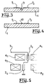
- this disadvantage is avoided, without the need to provide a substrate distinct for each of the channels V1 and V2, by the fact that a groove longitudinal, or groove, 9 is hollowed out longitudinally in the single substrate 1, so as to physically and surface separate channels V1 and V2. Surface waves then only propagate practically no one way to another, however the connections between channels can for example be carried out without problems by wire connection technique over this groove 9.
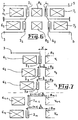
- the input transducers 2 1 , 2 2 on the one hand, and the output transducers 4 1 , 4 2 on the other hand, are electrically connected in parallel. Their admittances are added, which reduces the output impedance: such a configuration is well suited to low impedance outputs.
- connection mode is optional, and that all other configurations are feasible from the point of view electric without changing the result due to the invention: series-series configuration (inputs and outputs respectively), parallel-series, series-parallel, differential assemblies with midpoint connected or not to earth, etc ...
- FIG. 5 shows for example, for this filter according to FIG. 2, a series configuration of the input transducers 2 1 , 2 2 .
- the same configuration being used for the output transducers (not shown), it is this time the impedances which are added, consequently increasing the output impedance of the filter: this configuration is suitable for high impedance outputs.
- connection is given in figure 6, where it it is a connection in differential mounting, such mounting being suitable for this type of electronics where the circuits are supplied so symmetrical with respect to mass; etc ...
- the transfer function of the filter is of the form: R. sin 2 ⁇ .
- the adaptation circuits adapt, at this frequency, the source and load impedances to the impedance that couples of transducers with their associated external networks.
- the reflection coefficient of the central reflector should be close to -3dB, which corresponds to as much reflected energy as of transmitted energy.
- this weighting will for example be obtained by deleting sources (the sources being the reflectors) and we will adjust the number of reflectors to have a reflection coefficient close to -3dB. According to the number sources removed, the network is more or less "subsampled", that is to say that there are free spaces between the reflectors.
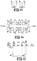
- the weighting can also be obtained by forming groups of reflectors which are shifted slightly to weight the reflection coefficient specific to each group as shown in FIG. 13 for a group i with an offset e 1 and a group i + 1 with an offset e 2 .
- the distances between input transducer 2 and central reflector 8 are: X for channel V1 X + ⁇ / 2N for channel V2 X + ⁇ / N for channel V3 X + (N-2) . ⁇ / 2N for channel VN-1 and X + (N-1) . ⁇ / 2N for the VN channel.
- the transfer function of the filter is equal to the sum of all contributions.
- N symmetrical channels (noted from 1 to N) and shifted by X + 2n - (N + 1) 2N (kN + 1), it is of the form: where R is the reflection coefficient of the networks ⁇ , the phase corresponding to the average inter-transducer distance and Tea 1 and Tea 2 the electro-acoustic transfer functions of the set consisting of the input and output transducers and the networks rear reflective.
- the filtering functions Fn are all zero at the central frequency with the exception of FN. We can thus see how all the reflectors participate directly in the transfer function.
- N even is preferable for benefit from an additional rejection due to the response of the central reflector, because ⁇ tends to 0 outside the bandwidth.
- the optimal value of the reflection coefficient of the central reflector at the frequency of the passband is
- sin ( ⁇ / 2N) for N even.
- ⁇ 0 is a first solution.
- This solution corresponds to the absence of a central reflector and is therefore not in accordance with the invention as defined in the claims.
- the other optimal solution is
- sin ( ⁇ / 2N) .
- the transfer function of the filter is of the form: R N-1 ⁇ Sin (N D ) (for N even).
- the only non-zero contribution to the central frequency is the last term linked to the Nth path (this is the principle of the structure)
- the troublesome contributions via this effect are those of the odd order paths (giving rise to cosines) and more particularly the direct path which is not at all filtered by rear reflectors.
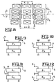
- a variant of the present invention consists in parallel two multi-lane structures according to Figure 2, and more generally according to Figure 7, these structures being of the same type, but the offsets of the direct paths varying in opposite directions from a structure to the other with respect to the longitudinal axis Y of symmetry of the assembly and as and as we move away from it, although the relative shifts between channels are equal in absolute values for each of these two structures.
- this variant amounts to making a filter using two previous structures, each with N channels, so as to provide additional rejection on all the paths of odd order, while in no way affecting the other paths.
- the inter-transducer distances of the N channels of the two structures follow the following arithmetic progressions, making it possible to provide a phase shift between structures equal to an even multiple of ⁇ for the paths of even order and equal to a multiple odd of ⁇ for odd order paths (including direct path):
- the new form of the transfer function is then approximately as follows: form on which one effectively notes the additional filtering operated on the paths of odd order by the intermediary of the last term in cosine.
- FIG 8. A simple example of embodiment applied to the latter case is shown in Figure 8.
- This is a filter in this case realizing the paralleling of two structures S1, S2 both similar to the structure according to Figure 2, but where the inter-transducer distances are: X - ⁇ / 2 and X for the structure S1; and X and X + ⁇ / 2 for structure S2, which gives a difference of ⁇ / 2 for all direct paths of the same rank.
- Figures 9 to 12 show respectively four types of possible connections: series-series, parallel-parallel, parallel-series, and differential mounting (in this last variant, the connection of the midpoint to ground is not mandatory).
- the quality coefficient of a transducer is defined as the ratio of the susceptance of the transducer to its conductance. This coefficient is k 2 / M, where k 2 is the piezoelectric coupling coefficient of the material and M the number of active electrodes of the transducer. As we wish to decrease this sensitivity, for a given material we are led to increase M.
- FIG. 14 The general structure shown in FIG. 14 is therefore obtained, comprising two central reflectors 8 1 and 8 2 and four transducers / reflectors of the DART type. 62 1 , 62 2 , 47 1 and 47 2 . This applies to all variants, in particular those of Figures 9 to 12 which will be described later.
- a DART structure is known from the French patent No. 2,653,632 filed by the Claimant on October 20, 1989.
- the simplest version of the basic cell of this structure is shown in Figure 15. This version includes a cell transmitter with 3 electrodes and a reflective cell with 2 electrodes.
- EWC Electrode Width Control
- This structure compared to the previous structure the advantages of not generating sub-harmonics and allowing a better reflection-transduction compromise.
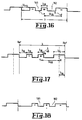
- FIG. 16 constitutes the basic cell where the centers of transduction T and of reflection R are placed respectively in the center of the electrode + and in the center of the reflector.
- this structure is not optimal, since the + electrode being surrounded by 2 different inter-electrode spaces 161 and 162, its transduction center is not exactly at the center of this electrode.
- another structure consists in shifting the source (that is to say the 2 electrodes at ⁇ / 8 by a distance ⁇ x from the position at 3 ⁇ / 8.
- the reflections on the 2 electrodes width ⁇ / 8) continue to be in phase opposition and an appropriate choice of ⁇ x makes it possible to place the transduction center at the optimal point (3 ⁇ / 8 from the reflector).
- the structure of the 2 DARTs is such that the coefficients of short-circuit reflection are equal. However, this condition does not impose not a complete identity of these 2 DARTs. So the transductions may be different. If you want to get better rejection by an additional filtering of the direct path one of the DART (or both) can be weighted by deleting sources (sources being the active electrodes), or by variable overlapping of the fingers. We prefer the latter, on a DART only, when we want to obtain a good distant rejection.
- the invention can also be extended, by replacing the "external transducer-reflector" assembly by any directive device (totally or partially unidirectional) such as transducer "3 phases "or group, bi-directional transducer placed inside a folded 3dB multi-path coupler; etc ...
- any directive device totally or partially unidirectional
Landscapes
- Physics & Mathematics (AREA)
- Acoustics & Sound (AREA)
- Surface Acoustic Wave Elements And Circuit Networks Thereof (AREA)
Claims (18)
- Filter mit akustischen Oberflächenwellen und Resonanzhohlräumen (61, 81; 71; 62, 82; 82, 72) in Längsrichtung, wobei das Filter N parallele Filterkanäle (V1, V2, ...) besitzt und N eine ganze Zahl mindestens gleich 2 ist, und wobei jeder Kanal einen Eingangstransduktor (21, 22, ...) und einen Ausgangstransduktor (41, 42, ...) aufweist, die zwischen sich eine direkte Strecke definieren, und mindestens zwei reflektierende Netze (61; 71) enthält, die für diesen Kanal mindestens einen Resonanzhohlraum in Längsrichtung definieren, wobei die Durchlaßamplituden zumindest für diese direkten Strecken praktisch die gleichen für diese N Kanäle sind, dadurch gekennzeichnet,und daß somit praktisch die Transferfunktion als Verzögerungsleitung außerhalb des Sperrbands des Filters zu Null wird.N eine gerade Zahl größer oder gleich zwei ist,daß der Unterschied in der Ausbreitungslänge auf der direkten Strecke für zwei aufeinanderfolgende Kanäle (V1, V2) im wesentlichen, abgesehen von einem ganzzahligen Vielfachen der Wellenlänge (λ) bei der zentralen Filterfrequenz (fo), dem N-ten Teil dieser Wellenlänge (λ) gleicht, so daß für diese zentrale Frequenz (fo) die Vektorresultierende der Signale dieser N Kanäle, die den direkten Strecken entsprechen, praktisch Null ist,und daß jeder Kanal einen zentralen Reflektor (81, 82) besitzt,
- Filter mit akustischen Oberflächenwellen und Resonanzhohlräumen (61, 81; 71; 62, 82; 82, 72) in Längsrichtung, wobei das Filter N parallele Filterkanäle (V1, V2, ...) besitzt und N eine ganze Zahl mindestens gleich 2 ist, und wobei jeder Kanal einen Eingangstransduktor (21, 22, ...) und einen Ausgangstransduktor (41, 42, ...) aufweist, die zwischen sich eine direkte Strecke definieren, und mindestens zwei reflektierende Netze (61; 71) enthält, die für diesen Kanal mindestens einen Resonanzhohlraum in Längsrichtung definieren, wobei die Durchlaßamplituden zumindest für diese direkten Strecken praktisch die gleichen für diese N Kanäle sind, dadurch gekennzeichnet,und daß somit praktisch die Transferfunktion als Verzögerungsleitung außerhalb des Sperrbands des Filters zu Null wird.daß N eine ungerade Zahl größer oder gleich drei ist,daß der Unterschied in der Ausbreitungslänge auf der direkten Strecke für zwei aufeinanderfolgende Kanäle (V1, V2) im wesentlichen, abgesehen von einem ganzzahligen Vielfachen der Wellenlänge (λ) bei der zentralen Filterfrequenz (fo), dem N-ten Teil dieser Wellenlänge (λ) gleicht, so daß für diese zentrale Frequenz (fo) die Vektorresultierende der Signale dieser N Kanäle, die den direkten Strecken entsprechen, praktisch Null ist,
- Filter nach Anspruch 1 oder 2, dadurch gekennzeichnet, daß jede Gruppe aus einem Transduktor und einem Reflektor netz eine gemeinsame Vorrichtung vom Typ DART (621-472) bildet.
- Filter nach einem der Ansprüche 1 bis 3, dadurch gekennzeichnet, daß die Reflexionskoeffizienten der DART-Vorrichtungen (621-472) im Kurzschluß gleich sind.
- Filter nach einem beliebigen der Ansprüche 3 und 4, dadurch gekennzeichnet, daß mindestens eine der DART-Vorrichtungen (621-472) durch Unterdrückung von Quellen gewichtet ist.
- Filter nach einem beliebigen der Ansprüche 3 und 4, dadurch gekennzeichnet, daß mindestens eine der DART-Vorrichtungen (621-472) durch eine variable Überdeckung der Finger gewichtet ist.
- Filter nach einem beliebigen der Ansprüche 3 bis 6, dadurch gekennzeichnet, daß mindestens eine der DART-Vorrichtungen (621-472) vom EWC-Typ mit einer Verschiebung von λ/48 ist.
- Filter nach einem beliebigen der Ansprüche 3 bis 6, dadurch gekennzeichnet, daß mindestens eine der DART-Vorrichtungen (621-472) vom EWC-Typ mit einer Verschiebung von -λ/16 ist.
- Filter nach einem beliebigen der Ansprüche 3 bis 6, dadurch gekennzeichnet, daß mindestens eine der DART-Vorrichtungen (621-472) aus einer Gruppe von abwechselnden Sendezellen und Reflektorzellen gebildet wird, wobei jede Sendezelle drei Elektroden einer Breite λ/6 besitzt, die einen Abstand von 3λ/4 über eine Strecke gleich λ mit zwei inaktiven Elektroden gefolgt von einer aktiven Elektrode aufweisen, während jede Reflektorzelle zwei inaktive Elektroden der Breite λ/4 in einem Abstand von 3λ/8 über eine Strecke gleich λ besitzt.
- Oberflächenwellenfilter nach einem beliebigen der Ansprüche 1 bis 9, dadurch gekennzeichnet, daß es auf einem gemeinsamen Substrat (1) ausgebildet ist und daß eine Längsrinne (9) in dieses Substrat zwischen jeweils zwei benachbarte Kanäle (V1, V2, ...) eingeschnitten ist, um sie gegenseitig für die akustischen Oberflächenwellen zu isolieren.
- Oberflächenwellenfilter nach einem beliebigen der Ansprüche 1 bis 9, dadurch gekennzeichnet, daß es auf einem gemeinsamen Substrat (1) ausgebildet ist und daß eine Längsschicht (10) aus einem die akustischen Oberflächenwellen absorbierenden Material zwischen je zwei Kanäle (V1, V2, ...) aufgebracht ist.
- Oberflächenwellenfilter nach einem beliebigen der Ansprüche 1 bis 11, dadurch gekennzeichnet, daß jeder dieser Kanäle (V1, V2, ...) bezüglich der Mittellinie (L) des Raums zwischen den Transduktoren symmetrisch ist.
- Oberflächenwellenfilter nach Anspruch 1, dadurch gekennzeichnet, daß jeder der Kanäle einen zentralen Reflektor (8) und zwei äußere Reflektoren (6, 7) enthält.
- Oberflächenwellenfilter nach einem der Ansprüche 1 bis 13, dadurch gekennzeichnet, daß für eine zusätzliche Sperrung auf der direkten Strecke für die Frequenzen, die im Sperrband von der zentralen Frequenz (fo) abweichen, das Filter aus der parallelen Anordnung von zwei solchen oben erwähnten Strukturen (S1, S2) mit mehreren Kanälen gebildet wird, wobei diese Strukturen vom gleichen Typ sind, aber Verschiebungen der direkten Strecken (
- Filter nach einem beliebigen der Ansprüche 1 bis 13, dadurch gekennzeichnet, daß die Anzahl von Elektroden des zentralen Reflektors (81, 82) so gewählt ist, daß der Reflexionskoeffizient im wesentlichen den Wert -3dB besitzt.
- Filter nach Anspruch 15, dadurch gekennzeichnet, daß der zentrale Reflektor (81, 82) außerdem durch Unterdrückung von Elektroden gewichtet ist und neutrale Zellen besitzt, die die unterdrückten Elektroden ersetzen, um einen konstanten Metallisierungsgrad beizubehalten.
- Oberflächenwellenfilter nach einem beliebigen der Ansprüche 1 bis 16, dadurch gekennzeichnet, daß es auf einem gemeinsamen Substrat (1) ausgebildet ist und daß die Kanäle (V1, V2, ...) in Längsrichtung gegeneinander so versetzt sind, daß die Kopplungen zwischen diesen Kanälen durch die Gegenphasigkeit zu Null werden.
- Filter nach einem beliebigen der Ansprüche 1 bis 17, dadurch gekennzeichnet, daß es keine besondere Maßnahmen gegen die Volumenwellen des Substrats gibt, auf dem die Organe des Filters ausgebildet sind.
Applications Claiming Priority (3)
| Application Number | Priority Date | Filing Date | Title |
|---|---|---|---|
| FR9112882 | 1991-10-18 | ||
| FR9112882A FR2682833B1 (fr) | 1991-10-18 | 1991-10-18 | Filtre a ondes de surface et a trajet acoustique replie. |
| PCT/FR1992/000827 WO1993008641A1 (fr) | 1991-10-18 | 1992-08-28 | Filtre a ondes de surface et a trajet acoustique replie |
Publications (3)
| Publication Number | Publication Date |
|---|---|
| EP0608249A1 EP0608249A1 (de) | 1994-08-03 |
| EP0608249B1 EP0608249B1 (de) | 1995-10-11 |
| EP0608249B2 true EP0608249B2 (de) | 2000-04-12 |
Family
ID=9418079
Family Applications (1)
| Application Number | Title | Priority Date | Filing Date |
|---|---|---|---|
| EP92918770A Expired - Lifetime EP0608249B2 (de) | 1991-10-18 | 1992-08-28 | Oberflächenwellenfilter mit einem gefalteten akustischen pfad |
Country Status (6)
| Country | Link |
|---|---|
| US (1) | US5475348A (de) |
| EP (1) | EP0608249B2 (de) |
| CA (1) | CA2121477C (de) |
| DE (1) | DE69205437T3 (de) |
| FR (1) | FR2682833B1 (de) |
| WO (1) | WO1993008641A1 (de) |
Families Citing this family (51)
| Publication number | Priority date | Publication date | Assignee | Title |
|---|---|---|---|---|
| JP3001350B2 (ja) * | 1993-05-19 | 2000-01-24 | 日本電気株式会社 | 弾性表面波フィルタ |
| US5793146A (en) * | 1993-11-12 | 1998-08-11 | Rf Monolithics, Inc. | Surface acoustic wave transducer having selected reflectivity |
| FR2712752B1 (fr) * | 1993-11-16 | 1995-12-22 | Thomson Csf | Filtres à ondes de surface à trajet acoustique replié. |
| US5426339A (en) * | 1994-04-01 | 1995-06-20 | Rf Monolithics, Inc. | Surface acoustic wave devices with mode changing characteristics |
| GB2289180B (en) * | 1994-04-25 | 1998-08-12 | Advanced Saw Prod Sa | Saw filter |
| GB2289181B (en) * | 1994-04-25 | 1998-08-12 | Advanced Saw Prod Sa | Saw filter |
| JP3606944B2 (ja) * | 1994-04-25 | 2005-01-05 | ノキア コーポレイション | Sawフィルタ |
| GB2288937B (en) * | 1994-04-25 | 1998-06-10 | Advanced Saw Prod Sa | SAW filter |
| DE4419722C1 (de) | 1994-06-06 | 1996-02-22 | Siemens Ag | Mit akustischen Oberflächenwellen arbeitendes Filter |
| EP0704967B1 (de) * | 1994-09-28 | 2001-08-08 | Masao Takeuchi | Akustische Oberflächenwellenanordnung |
| US5545940A (en) * | 1994-11-07 | 1996-08-13 | Rf Monolithics, Inc. | Multitrack transversely folded surface acoustic wave structure |
| US5835990A (en) * | 1995-06-16 | 1998-11-10 | Northern Telecom Limited | Longitudinally coupled double mode surface wave resonators |
| FR2739232B1 (fr) * | 1995-09-26 | 1997-10-24 | Thomson Csf | Filtre a ondes acoustiques de surface utilisant le couplage de trois voies acoustiques |
| FR2740908B1 (fr) * | 1995-11-07 | 1997-11-28 | Thomson Csf | Transducteur a ondes acoustiques de surface attaque en differentiel |
| DE19547470C2 (de) * | 1995-12-19 | 1998-01-15 | Siemens Matsushita Components | Mit akustischen Oberflächenwellen arbeitendes Filter-OFW-Filter |
| US5793266A (en) * | 1996-08-12 | 1998-08-11 | Motorola Inc. | Differential input and/or differential output, transversely-coupled surface acoustic wave filter |
| DE19638455A1 (de) | 1996-09-19 | 1998-04-02 | Siemens Matsushita Components | Twin-Dualmode-Filter |
| DE19638370C2 (de) * | 1996-09-19 | 2001-06-13 | Epcos Ag | Oberflächenwellenfilter für unsymmetrische/symmetrische und symmetrische/symmetrische Betriebsweise |
| JP3186604B2 (ja) | 1996-10-09 | 2001-07-11 | 株式会社村田製作所 | 弾性表面波フィルタ装置 |
| US5831494A (en) * | 1996-12-12 | 1998-11-03 | Sawtek Inc. | Dual track low-loss reflective saw filter |
| FR2762458B1 (fr) * | 1997-04-18 | 1999-07-09 | Thomson Csf | Dispositif a ondes acoustiques de surface a couplage par proximite a entrees/sorties differentielles |
| US5896071A (en) * | 1997-05-15 | 1999-04-20 | Northern Telecom Limited | Surface wave device balun resonator filters |
| US6104260A (en) * | 1997-12-22 | 2000-08-15 | Matsushita Electric Industrial Co., Ltd. | Surface acoustic wave filter with first and second filter tracks and balanced or unbalanced terminals |
| FR2774826B1 (fr) | 1998-02-06 | 2000-05-05 | Thomson Csf | Filtre a resonateurs a ondes acoustiques de surface |
| DE19837743B4 (de) * | 1998-08-20 | 2009-11-26 | Leibniz-Institut Für Festkörper- Und Werkstoffforschung Dresden E.V. | Akustisches Oberflächenwellenfilter |
| FR2785473B1 (fr) * | 1998-10-30 | 2001-01-26 | Thomson Csf | Filtre faibles pertes a ondes acoustiques de surface sur substrat de quartz de coupe optimisee |
| RU2157046C2 (ru) * | 1998-12-24 | 2000-09-27 | Омский научно-исследовательский институт приборостроения | Фильтр на поверхностных акустических волнах |
| RU98123756A (ru) * | 1998-12-29 | 2000-10-20 | Моторола Инк. (US) | Трехканальный фильтр на поверхностных акустических волнах |
| RU2159986C1 (ru) * | 1999-03-29 | 2000-11-27 | Швец Валерий Борисович | Реверсный преобразователь с естественной направленностью излучения поверхностных акустических волн (варианты) |
| RU2158475C1 (ru) * | 1999-04-29 | 2000-10-27 | Швец Валерий Борисович | Реверсный преобразователь с естественной направленностью излучения поверхностных акустических волн (варианты) |
| JP3338839B2 (ja) | 1999-06-04 | 2002-10-28 | エヌ・アール・エス・テクノロジー株式会社 | 一方向性弾性表面波変換器 |
| EP1150425B1 (de) * | 1999-10-04 | 2008-02-20 | Kabushiki Kaisha Toshiba | Obreflächenwellenanordnung |
| RU2171010C2 (ru) * | 1999-10-12 | 2001-07-20 | Данилов Александр Львович | Фильтр на поверхностных акустических волнах с квазивеерными преобразователями |
| RU2158056C1 (ru) * | 1999-10-12 | 2000-10-20 | Швец Валерий Борисович | Высокочастотный реверсный преобразователь с "естественной" направленностью излучения поверхностных акустических волн |
| JP2001196898A (ja) * | 2000-01-05 | 2001-07-19 | Fujitsu Ltd | 弾性表面波フィルタ |
| DE10026074B4 (de) * | 2000-05-25 | 2010-02-18 | Epcos Ag | Rekursives OFW-Filter mit geringer Chiplänge |
| JP3687566B2 (ja) * | 2000-07-25 | 2005-08-24 | 株式会社村田製作所 | 縦結合共振子型弾性表面波フィルタ |
| WO2002058233A1 (en) * | 2001-01-18 | 2002-07-25 | Infineon Technologies Ag | Filter devices and method for fabricating filter devices |
| JP4079658B2 (ja) * | 2002-03-05 | 2008-04-23 | 株式会社リコー | 2値化ウォブル信号を生成する回路、ライトクロック生成回路、2値化ウォブル信号を生成する方法、ライトクロック生成方法及び光ディスク装置 |
| FR2837636B1 (fr) * | 2002-03-19 | 2004-09-24 | Thales Sa | Dispositif a ondes acoustiques d'interface en tantalate de lithium |
| US6842091B2 (en) * | 2003-02-28 | 2005-01-11 | Northrop Grumman Corporation | Weighted SAW reflector grating using dithered acoustic reflectors |
| US6836197B2 (en) * | 2003-02-28 | 2004-12-28 | Northrop Grumman Corporation | Dual track SAW reflector filter using weighted reflective gratings |
| US6847272B2 (en) * | 2003-02-28 | 2005-01-25 | Northrop Grumman Corporation | Weighted SAW reflector using distributed acoustic reflective dots |
| FR2864618B1 (fr) * | 2003-12-24 | 2006-03-03 | Temex Sa | Capteur de temperature ou de temperature et de pression interrogeable a distance |
| DE102009009484B4 (de) * | 2009-02-19 | 2014-07-17 | Epcos Ag | Zweikanal-SAW Filter |
| RU2439755C1 (ru) * | 2010-05-13 | 2012-01-10 | Открытое акционерное общество "Концерн "Созвездие" | Фоточувствительный фильтр на поверхностных акустических волнах |
| US10381998B2 (en) | 2015-07-28 | 2019-08-13 | Qorvo Us, Inc. | Methods for fabrication of bonded wafers and surface acoustic wave devices using same |
| US10128814B2 (en) | 2016-01-28 | 2018-11-13 | Qorvo Us, Inc. | Guided surface acoustic wave device providing spurious mode rejection |
| US10084427B2 (en) | 2016-01-28 | 2018-09-25 | Qorvo Us, Inc. | Surface acoustic wave device having a piezoelectric layer on a quartz substrate and methods of manufacturing thereof |
| US11206007B2 (en) | 2017-10-23 | 2021-12-21 | Qorvo Us, Inc. | Quartz orientation for guided SAW devices |
| FR3127660A1 (fr) | 2021-09-27 | 2023-03-31 | Frec'n'sys | Filtre a ondes elastiques de surface et a cavites resonantes |
Family Cites Families (10)
| Publication number | Priority date | Publication date | Assignee | Title |
|---|---|---|---|---|
| US3946342A (en) * | 1973-08-10 | 1976-03-23 | Texas Instruments Incorporated | Weighting surface wave filters by withdrawing electrodes |
| US4004254A (en) * | 1975-04-03 | 1977-01-18 | Zenith Radio Corporation | Swif with side lobe compensation barrier |
| GB1585087A (en) * | 1976-07-29 | 1981-02-25 | Plessey Co Ltd | Surface acoustic wave filters |
| US4390854A (en) * | 1981-03-03 | 1983-06-28 | The United States Of America As Represented By The Secretary Of The Air Force | Broad bandwidth surface acoustic wave filter apparatus with staggered tuning |
| US4609891A (en) * | 1985-10-16 | 1986-09-02 | Sperry Corporation | Staggered SAW resonator for differential detection |
| US4764701A (en) * | 1986-12-30 | 1988-08-16 | Zenith Electronics Corporation | Multichannel surface acoustic wave encoder/decoder |
| US5264751A (en) * | 1989-10-20 | 1993-11-23 | Thomson-Csf | Unilateral surface wave transducer |
| FR2653632B1 (fr) * | 1989-10-20 | 1991-12-20 | Thomson Csf | Transducteur d'ondes de surface unidirectionnel. |
| EP0508325A1 (de) * | 1991-04-11 | 1992-10-14 | SIEMENS MATSUSHITA COMPONENTS GmbH & CO. KG | Reflektive Verzögerungsleitung in Oberflächenwellentechnik |
| US5296624A (en) * | 1992-11-25 | 1994-03-22 | Huls America, Inc. | Preparation of sterically-hindered organosilanes |
-
1991
- 1991-10-18 FR FR9112882A patent/FR2682833B1/fr not_active Expired - Fee Related
-
1992
- 1992-08-28 WO PCT/FR1992/000827 patent/WO1993008641A1/fr not_active Ceased
- 1992-08-28 EP EP92918770A patent/EP0608249B2/de not_active Expired - Lifetime
- 1992-08-28 CA CA002121477A patent/CA2121477C/fr not_active Expired - Fee Related
- 1992-08-28 DE DE69205437T patent/DE69205437T3/de not_active Expired - Lifetime
- 1992-10-28 US US08/211,622 patent/US5475348A/en not_active Expired - Lifetime
Also Published As
| Publication number | Publication date |
|---|---|
| US5475348A (en) | 1995-12-12 |
| EP0608249A1 (de) | 1994-08-03 |
| DE69205437T3 (de) | 2000-08-24 |
| FR2682833A1 (fr) | 1993-04-23 |
| CA2121477A1 (fr) | 1993-04-29 |
| DE69205437D1 (de) | 1995-11-16 |
| FR2682833B1 (fr) | 1993-12-03 |
| EP0608249B1 (de) | 1995-10-11 |
| DE69205437T2 (de) | 1996-03-21 |
| WO1993008641A1 (fr) | 1993-04-29 |
| CA2121477C (fr) | 2002-12-17 |
Similar Documents
| Publication | Publication Date | Title |
|---|---|---|
| EP0608249B2 (de) | Oberflächenwellenfilter mit einem gefalteten akustischen pfad | |
| EP0872954B1 (de) | Akustische Oberflächenwellenanordnung mit Nahfeldkopplung und differentiellen Ein- und Ausgängen | |
| EP1053593B1 (de) | Resonatorfilter mit akustischen oberflächenwellen | |
| EP3996275B1 (de) | Elektromechanische vorrichtung mit einstellbarer resonanzfrequenz | |
| EP0513085B2 (de) | Akustische oberflächenwellenfilter | |
| FR2601824A1 (fr) | Filtre d'onde elastique de surface | |
| EP0660981B1 (de) | Wandler für unidirektionale Weller | |
| WO2008155346A1 (fr) | Resonateur a ondes de surface a resonance parasite reduite | |
| EP0369835B1 (de) | Wandler für ein akustisches Oberflächenwellen-Filter | |
| FR2468255A1 (fr) | Dispositifs a ondes acoustiques de surface et systemes comportant de tels dispositifs | |
| EP0862813B1 (de) | Differenzbetriebener wandler für akustische oberflächenwellen | |
| CA2280422C (fr) | Filtre acoustique a deux canaux differents a compensation de rejection | |
| EP0424240B1 (de) | Richtwandler für Oberflächenwellen | |
| FR2685580A1 (fr) | Filtre a ondes de surface. | |
| WO1995014332A1 (fr) | Filtre a ondes de surface a trajet acoustique replie | |
| EP0576340B1 (de) | Oberflächenwellenfilter mit reflektierenden Gittern | |
| FR3162108A1 (fr) | Dispositif à ondes élastiques |
Legal Events
| Date | Code | Title | Description |
|---|---|---|---|
| PUAI | Public reference made under article 153(3) epc to a published international application that has entered the european phase |
Free format text: ORIGINAL CODE: 0009012 |
|
| 17P | Request for examination filed |
Effective date: 19940418 |
|
| AK | Designated contracting states |
Kind code of ref document: A1 Designated state(s): CH DE FR GB LI SE |
|
| 17Q | First examination report despatched |
Effective date: 19950123 |
|
| GRAA | (expected) grant |
Free format text: ORIGINAL CODE: 0009210 |
|
| AK | Designated contracting states |
Kind code of ref document: B1 Designated state(s): CH DE FR GB LI SE |
|
| REF | Corresponds to: |
Ref document number: 69205437 Country of ref document: DE Date of ref document: 19951116 |
|
| GBT | Gb: translation of ep patent filed (gb section 77(6)(a)/1977) |
Effective date: 19951216 |
|
| PLBQ | Unpublished change to opponent data |
Free format text: ORIGINAL CODE: EPIDOS OPPO |
|
| PLBI | Opposition filed |
Free format text: ORIGINAL CODE: 0009260 |
|
| PLBF | Reply of patent proprietor to notice(s) of opposition |
Free format text: ORIGINAL CODE: EPIDOS OBSO |
|
| 26 | Opposition filed |
Opponent name: SIEMENS MATSUSHITA COMPONENTS GMBH & CO. KG Effective date: 19960711 |
|
| PLBF | Reply of patent proprietor to notice(s) of opposition |
Free format text: ORIGINAL CODE: EPIDOS OBSO |
|
| PLBQ | Unpublished change to opponent data |
Free format text: ORIGINAL CODE: EPIDOS OPPO |
|
| PLAB | Opposition data, opponent's data or that of the opponent's representative modified |
Free format text: ORIGINAL CODE: 0009299OPPO |
|
| R26 | Opposition filed (corrected) |
Opponent name: SIEMENS MATSUSHITA COMPONENTS GMBH & CO. KG Effective date: 19960711 |
|
| PGFP | Annual fee paid to national office [announced via postgrant information from national office to epo] |
Ref country code: CH Payment date: 19980713 Year of fee payment: 7 |
|
| PLAW | Interlocutory decision in opposition |
Free format text: ORIGINAL CODE: EPIDOS IDOP |
|
| PG25 | Lapsed in a contracting state [announced via postgrant information from national office to epo] |
Ref country code: LI Free format text: LAPSE BECAUSE OF NON-PAYMENT OF DUE FEES Effective date: 19990831 Ref country code: CH Free format text: LAPSE BECAUSE OF NON-PAYMENT OF DUE FEES Effective date: 19990831 |
|
| PLAW | Interlocutory decision in opposition |
Free format text: ORIGINAL CODE: EPIDOS IDOP |
|
| PUAH | Patent maintained in amended form |
Free format text: ORIGINAL CODE: 0009272 |
|
| 27A | Patent maintained in amended form |
Effective date: 20000412 |
|
| AK | Designated contracting states |
Kind code of ref document: B2 Designated state(s): CH DE FR GB LI SE |
|
| REG | Reference to a national code |
Ref country code: CH Ref legal event code: PL |
|
| GBTA | Gb: translation of amended ep patent filed (gb section 77(6)(b)/1977) | ||
| REG | Reference to a national code |
Ref country code: GB Ref legal event code: IF02 |
|
| REG | Reference to a national code |
Ref country code: FR Ref legal event code: CD |
|
| PGFP | Annual fee paid to national office [announced via postgrant information from national office to epo] |
Ref country code: FR Payment date: 20080818 Year of fee payment: 17 |
|
| PGFP | Annual fee paid to national office [announced via postgrant information from national office to epo] |
Ref country code: GB Payment date: 20080827 Year of fee payment: 17 |
|
| PGFP | Annual fee paid to national office [announced via postgrant information from national office to epo] |
Ref country code: SE Payment date: 20080827 Year of fee payment: 17 |
|
| GBPC | Gb: european patent ceased through non-payment of renewal fee |
Effective date: 20090828 |
|
| PG25 | Lapsed in a contracting state [announced via postgrant information from national office to epo] |
Ref country code: GB Free format text: LAPSE BECAUSE OF NON-PAYMENT OF DUE FEES Effective date: 20090828 |
|
| PG25 | Lapsed in a contracting state [announced via postgrant information from national office to epo] |
Ref country code: SE Free format text: LAPSE BECAUSE OF NON-PAYMENT OF DUE FEES Effective date: 20090829 |
|
| REG | Reference to a national code |
Ref country code: FR Ref legal event code: ST Effective date: 20110729 |
|
| PG25 | Lapsed in a contracting state [announced via postgrant information from national office to epo] |
Ref country code: FR Free format text: LAPSE BECAUSE OF NON-PAYMENT OF DUE FEES Effective date: 20090831 |
|
| PGFP | Annual fee paid to national office [announced via postgrant information from national office to epo] |
Ref country code: DE Payment date: 20110818 Year of fee payment: 20 |
|
| REG | Reference to a national code |
Ref country code: DE Ref legal event code: R071 Ref document number: 69205437 Country of ref document: DE |
|
| REG | Reference to a national code |
Ref country code: DE Ref legal event code: R071 Ref document number: 69205437 Country of ref document: DE |
|
| PG25 | Lapsed in a contracting state [announced via postgrant information from national office to epo] |
Ref country code: DE Free format text: LAPSE BECAUSE OF EXPIRATION OF PROTECTION Effective date: 20120829 |