EP0608979A2 - Circuit de commutation - Google Patents
Circuit de commutation Download PDFInfo
- Publication number
- EP0608979A2 EP0608979A2 EP94300156A EP94300156A EP0608979A2 EP 0608979 A2 EP0608979 A2 EP 0608979A2 EP 94300156 A EP94300156 A EP 94300156A EP 94300156 A EP94300156 A EP 94300156A EP 0608979 A2 EP0608979 A2 EP 0608979A2
- Authority
- EP
- European Patent Office
- Prior art keywords
- gto
- circuit
- power
- winding
- capacitors
- Prior art date
- Legal status (The legal status is an assumption and is not a legal conclusion. Google has not performed a legal analysis and makes no representation as to the accuracy of the status listed.)
- Granted
Links
Images


Classifications
-
- H—ELECTRICITY
- H02—GENERATION; CONVERSION OR DISTRIBUTION OF ELECTRIC POWER
- H02M—APPARATUS FOR CONVERSION BETWEEN AC AND AC, BETWEEN AC AND DC, OR BETWEEN DC AND DC, AND FOR USE WITH MAINS OR SIMILAR POWER SUPPLY SYSTEMS; CONVERSION OF DC OR AC INPUT POWER INTO SURGE OUTPUT POWER; CONTROL OR REGULATION THEREOF
- H02M7/00—Conversion of AC power input into DC power output; Conversion of DC power input into AC power output
- H02M7/42—Conversion of DC power input into AC power output without possibility of reversal
- H02M7/44—Conversion of DC power input into AC power output without possibility of reversal by static converters
- H02M7/48—Conversion of DC power input into AC power output without possibility of reversal by static converters using discharge tubes with control electrode or semiconductor devices with control electrode
- H02M7/483—Converters with outputs that each can have more than two voltages levels
- H02M7/487—Neutral point clamped inverters
-
- H—ELECTRICITY
- H02—GENERATION; CONVERSION OR DISTRIBUTION OF ELECTRIC POWER
- H02P—CONTROL OR REGULATION OF ELECTRIC MOTORS, ELECTRIC GENERATORS OR DYNAMO-ELECTRIC CONVERTERS; CONTROLLING TRANSFORMERS, REACTORS OR CHOKE COILS
- H02P25/00—Arrangements or methods for the control of AC motors characterised by the kind of AC motor or by structural details
- H02P25/02—Arrangements or methods for the control of AC motors characterised by the kind of AC motor or by structural details characterised by the kind of motor
- H02P25/08—Reluctance motors
- H02P25/092—Converters specially adapted for controlling reluctance motors
-
- H—ELECTRICITY
- H02—GENERATION; CONVERSION OR DISTRIBUTION OF ELECTRIC POWER
- H02P—CONTROL OR REGULATION OF ELECTRIC MOTORS, ELECTRIC GENERATORS OR DYNAMO-ELECTRIC CONVERTERS; CONTROLLING TRANSFORMERS, REACTORS OR CHOKE COILS
- H02P9/00—Arrangements for controlling electric generators for the purpose of obtaining a desired output
Definitions
- This invention relates to switching circuits.
- the invention is particularly, though not exclusively, applicable to switching circuits for electric motors and generators.
- Electric motors and generators commonly rely on switching circuits for their control.
- a power converter typically provides pulses of unidirectional current in sequence to each of the phase windings. Similar sequential switching regimes are used to draw power from a switched reluctance generator.
- the source of the power for the converter is typically a capacitively smoothed direct voltage source - often referred to as a 'dc link' - which can be derived from a dc power supply or battery, or derived from a rectifier circuit which draws power from an ac source.
- the dc link is periodically switched to the windings of the switched reluctance motor/generator using semiconductor power switching devices.
- the semiconductor power switching devices through which the windings are energised have adequate voltage ratings to allow a single semiconductor device to be used in association with each phase as shown in Figure 1.
- Typical power converter circuits will be known to the skilled person and a variety of power switching devices is available, including bipolar transistors and field-effect transistors, insulated gate bipolar transistors, gate turn-off thyristors, MOS-controlled thyristors, static induction thyristors and other devices having the ability to switch between a high impedance OFF state and a lower impedance ON state and vice versa.
- Figure 1 illustrates a power converter system for one phase winding 1 of a switched reluctance motor.
- the unexcited winding 1 is suddenly connected to the dc link by the two power switching devices 3 and 4 which receive actuating signals at their respective control electrodes 5 and 6, the voltage across the winding changes suddenly from zero to V L , where V L is the link voltage.
- one of the two power switching devices 3 and 4 is switched off (say 3) by applying or removing the appropriate control signal to its control electrode, the winding current is compelled to flow through one of a pair of diodes 7 and 8 (say 8), respectively connected between each end of the winding and the opposite voltage dc link terminal, and the other power switching device 4 which remains actuated.
- the winding voltage changes suddenly from V L to approximately zero and the-current in the winding varies at a rate depending primarily on the current in the winding inductance, the value of the winding inductance itself, the rate of change of the winding inductance and on the resistance of the winding.
- both power switching devices are switched off simultaneously the winding current is compelled to flow through both diodes which are so connected to the dc link that the winding voltage changes suddenly from V L to -V L .
- a switching circuit for an inductive element comprising first and second terminals, capacitors serially connected between the first and second terminals and defining an electrical intermediate point between them, a pair of element connections, first power switch means comprising at least two power switches serially connected to conduct from the first terminal to one of the element connections, second power switch means, comprising at least two power switches serially connected to conduct from the other of the element connections to the second terminal, first diode means connected for conduction from the second terminal to the said one element connection, second diode means connected for conduction from the said other element connection to the first terminal, third and fourth diode means serially connected to conduct from between the power switching devices of the second power switch means to between the power switching devices of the first power switch means, the serial connection between the third and fourth diode means being connected with the intermediate point between the capacitors.
- each winding of, for example, a switched reluctance motor can be connected to the positive terminal of a capacitively smoothed direct voltage source via two power transistors or other semiconductor switches connected in series and the other end of each winding can be connected with the negative terminal of the direct voltage source via two further power transistors or other semiconductor switches connected in series.
- each winding end can be connected with the opposite polarity input terminal via the first and second circulating diodes (or two or more diodes in series in each case) with their conducting directions arranged so that they only return energy to the dc link.
- the smoothing capacitors are preferably arranged in one or more parallel connected series strings, each string preferably comprising an even number of capacitors of substantially equal value connected in series and having an electrical connection at the mid-point of the or each series string.
- the third diode means are connected to conduct from the or each mid-point to the common connection between the first pair of power transistors of the switching means.
- the fourth diode means are connected to conduct from the common connection between the second pair of power transistors or other switching means to the or each mid-point.
- the intermediate point is the position along the string of smoothing capacitors at which substantially equal voltages will be dropped across the capacitors connected between the intermediate point and each of the two terminals of the direct voltage source.
- an even number of capacitors of substantially equal capacitance and individual voltage rating may conveniently define a mid-point in the middle of a string, an odd number of capacitors having differing voltage ratings may equally well define such a mid-point depending on the value of the capacitors used.
- an intermediate point other than the mid-point may also be defined such that the power switching means are not exposed to damaging voltage magnitudes transiently or in their OFF states.
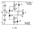
- Figure 2 shows an example of a power converter for one phase of a switched reluctance (SR) motor or generator according to the invention.
- SR switched reluctance
- V L an electrical power supply
- the driven rotor or other secondary element is mechanically driven to enhance the current in the windings which are sequentially switched to feed the generated power to a storage device or to drive electrical equipment.
- the positive and negative terminals 10 and 12 of a dc link have a string of four series connected capacitors 14 (of similar capacitance and voltage rating) connected between them.
- the connection between the middle two capacitors defines an electrical mid-point connection 16.
- a winding 18 of the SR motor has one end 20 connected, via two series connected gate turn-off (GTO) thyristors 22 and 24, to the positive terminal 10 and, via a diode 26 to the negative terminal 12.
- GTO thyristors 22 and 24 are connected to conduct from the positive terminal 10 to the end 20 of the winding 18 and the diode 26 is connected to conduct from the negative terminal 12 to the end 20.
- the other end 28 of the winding 18 is connected, via two series GTO thyristors 30 and 32 to the negative terminal and, via a diode 34 to the positive terminal 10.
- the GTO thyristors 30 and 32 are connected to conduct from the end 28 of the winding 18 to the negative terminal 12 and the diode 34 is connected to conduct from the end 28 to the positive terminal 10.
- the mid-point connection 16 is connected via a diode 36 to the common connection between the GTO's 22 and 24 and via a diode 38 to the common connection between the GTO's 30 and 32.
- the benefits provided by the invention are realised not by turning off the GTO thyristors 22 and 24 or 30 and 32 simultaneously, but in sequence.
- the GTO thyristor connected to a particular end of the winding is turned off after its associated GTO thyristor connected with the dc link.
- the GTO thyristor connected to a particular end of the winding is turned on before its associated GTO thyristor connected with the dc link.
- the circuit of Figure 2 ensures that each GTO thyristor will only be exposed to an OFF state voltage which is approximately half of the dc link voltage appearing across the string of capacitors 14.
- the turn-off and turn-on sequences for the four GTO thyristors follow a prescribed pattern, examples of which are described below.
- the voltage at the mid-point 16 then ceases changing negatively and the winding current circulates through the GTO 30, the diodes 38 and 36, and the GTO 22 with substantially zero voltage across the winding 18.
- the GTO 22 is then turned off, forcing the winding current to transfer to the diode 26. Winding current then flows via the GTO 30, and the diode 38 to the mid-point 16 causing the voltage of the mid-point 16 to change slightly positively.
- the GTO 30 is then turned off after a further delay during which the voltage at the mid-point 16 has returned to its desired value approximately midway between the potentials at the terminals 10 and 12.
- the time delays between turning off (or on) GTO's 24 and 32 and GTO's 22 and 30 can be conveniently determined by the voltage excursions of the mid-point 16 or by other means or measurements whereby the voltage at the mid-point 16 is maintained at substantially half V L or at least within prescribed safe limits.
- the purpose of the invention is to avoid exposing the GTO's to a damagingly large voltage and the voltage of the mid-point need not necessarily be maintained at half of V L during switch-over to achieve this.
- the turn-on sequence involves turning on three of the four GTO's, omitting GTO 24 or 32 initially. This applies half of the dc link voltage V L to the motor winding, but causes the mid-point 16 to change its potential either negatively or positively, depending on which GTO is omitted. Assuming the GTO 24 was initially not turned on, to restore the mid-point potential, the omitted GTO 24 is turned on and the GTO 32 is turned off until the mid-point 16 potential has been restored to its desired value approximately midway between the potentials of the terminals 10 and 12 of the direct voltage source.
- the other (non-conducting) GTO 32 is reactuated so that winding current is drawn from the direct voltage source not from (or directed to) the mid-point 16.
- successive turn-on sequences can alternate between that in which GTO 24 is omitted initially and that in which GTO 32 is omitted initially. This would ensure that any change in voltage at the midpoint 16 caused by a particular turn-on sequence is removed by the next turn-on sequence, thus ensuring that there is no progressive change in potential at the midpoint 16.
- Additional phase windings of an SR motor or generator with their own sets of power semiconductor devices can conveniently use the same string (or sets of strings in parallel) of capacitors or can be provided with their own independent strings of capacitors. Where the same strings of capacitors serve all phases of the SR motor or generator, the switching sequences of all phases can be coordinated to limit the voltage excursions of the mid-point 16, maintaining its potential between prescribed limits.
- FIG 3 shows a switching circuit for a 3-phase switched reluctance motor or generator.
- the circuit comprises three switching circuits, A, B and C as shown in Figure 2 all connected in parallel with the terminals D and E and to the midpoint F between series connected capacitors E.
- a controller H is arranged to actuate the sequential switching of the power switching devices in an appropriate sequence(s).
- two or more separately powered sources of direct voltage each capacitively smoothed, and in series with each other, may be used with their common connection(s) providing the mid-point or intermediate points to which diodes or diode strings are connected.
- the provision of separately powered sources of direct voltage removes the need to incorporate means for measuring and maintaining the voltage(s) at the said mid-point or intermediate points within prescribed limits.
Landscapes
- Engineering & Computer Science (AREA)
- Power Engineering (AREA)
- Control Of Electric Motors In General (AREA)
Applications Claiming Priority (2)
| Application Number | Priority Date | Filing Date | Title |
|---|---|---|---|
| GB9300734 | 1993-01-14 | ||
| GB939300734A GB9300734D0 (en) | 1993-01-14 | 1993-01-14 | High voltage power converters for switched reluctance motors |
Publications (3)
| Publication Number | Publication Date |
|---|---|
| EP0608979A2 true EP0608979A2 (fr) | 1994-08-03 |
| EP0608979A3 EP0608979A3 (en) | 1996-02-07 |
| EP0608979B1 EP0608979B1 (fr) | 1998-06-10 |
Family
ID=10728762
Family Applications (1)
| Application Number | Title | Priority Date | Filing Date |
|---|---|---|---|
| EP94300156A Expired - Lifetime EP0608979B1 (fr) | 1993-01-14 | 1994-01-10 | Circuit de commutation |
Country Status (4)
| Country | Link |
|---|---|
| US (1) | US5504410A (fr) |
| EP (1) | EP0608979B1 (fr) |
| DE (1) | DE69410836T2 (fr) |
| GB (1) | GB9300734D0 (fr) |
Cited By (3)
| Publication number | Priority date | Publication date | Assignee | Title |
|---|---|---|---|---|
| US6384564B1 (en) | 1999-06-22 | 2002-05-07 | University Of Warwick | Electrical machines |
| CN105191107A (zh) * | 2013-06-14 | 2015-12-23 | 富士电机株式会社 | 多电平逆变器 |
| CN105531921A (zh) * | 2014-04-03 | 2016-04-27 | 富士电机株式会社 | 安全控制装置 |
Families Citing this family (6)
| Publication number | Priority date | Publication date | Assignee | Title |
|---|---|---|---|---|
| GB9507540D0 (en) * | 1995-04-11 | 1995-05-31 | Switched Reluctance Drives Ltd | Control circuit and system for a switched reluctance machine and method of operating |
| GB9513916D0 (en) * | 1995-07-07 | 1995-09-06 | Switched Reluctance Drives Ltd | Switching circuit for an inductive load |
| US6812811B2 (en) * | 2002-05-14 | 2004-11-02 | Halliburton Energy Services, Inc. | Power discriminating systems |
| US7201244B2 (en) * | 2003-10-03 | 2007-04-10 | Letourneau, Inc. | Vehicle for materials handling and other industrial uses |
| US7782007B2 (en) * | 2007-05-22 | 2010-08-24 | Hamilton Sundstrand Corporation | Electrodynamic machine control |
| JP5808630B2 (ja) * | 2011-09-28 | 2015-11-10 | 株式会社ミツバ | Srモータ用制御装置 |
Family Cites Families (7)
| Publication number | Priority date | Publication date | Assignee | Title |
|---|---|---|---|---|
| GB2105933B (en) * | 1981-09-08 | 1984-11-14 | Switched Reluctance Drives Ltd | Power conversion circuit |
| US4584506A (en) * | 1984-11-23 | 1986-04-22 | Polestar Magnetronics Inc. | Reluctance motor with electronically controlled stator windings |
| DE4029335A1 (de) * | 1990-09-15 | 1992-03-19 | Philips Patentverwaltung | Schaltungsanordnung zum kommutieren eines reluktanzmotors |
| US5289107A (en) * | 1992-03-30 | 1994-02-22 | General Electric Company | Switched reluctance generator system with fault recovery capability |
| JP3229897B2 (ja) * | 1992-04-13 | 2001-11-19 | 三菱電機株式会社 | 3レベル3相インバータ装置 |
| US5327069A (en) * | 1992-06-19 | 1994-07-05 | General Electric Company | Switched reluctance machine including permanent magnet stator poles |
| US5291115A (en) * | 1992-09-25 | 1994-03-01 | The Texas A&M University System | Method and apparatus for sensing the rotor position of a switched reluctance motor without a shaft position sensor |
-
1993
- 1993-01-14 GB GB939300734A patent/GB9300734D0/en active Pending
-
1994
- 1994-01-10 EP EP94300156A patent/EP0608979B1/fr not_active Expired - Lifetime
- 1994-01-10 DE DE69410836T patent/DE69410836T2/de not_active Expired - Fee Related
- 1994-01-13 US US08/180,957 patent/US5504410A/en not_active Expired - Fee Related
Cited By (6)
| Publication number | Priority date | Publication date | Assignee | Title |
|---|---|---|---|---|
| US6384564B1 (en) | 1999-06-22 | 2002-05-07 | University Of Warwick | Electrical machines |
| CN105191107A (zh) * | 2013-06-14 | 2015-12-23 | 富士电机株式会社 | 多电平逆变器 |
| EP3010137A4 (fr) * | 2013-06-14 | 2017-03-15 | Fuji Electric Co., Ltd. | Onduleur à plusieurs niveaux |
| CN105191107B (zh) * | 2013-06-14 | 2018-03-30 | 富士电机株式会社 | 多电平逆变器 |
| CN105531921A (zh) * | 2014-04-03 | 2016-04-27 | 富士电机株式会社 | 安全控制装置 |
| CN105531921B (zh) * | 2014-04-03 | 2018-08-28 | 富士电机株式会社 | 安全控制装置 |
Also Published As
| Publication number | Publication date |
|---|---|
| GB9300734D0 (en) | 1993-03-03 |
| DE69410836D1 (de) | 1998-07-16 |
| EP0608979B1 (fr) | 1998-06-10 |
| DE69410836T2 (de) | 1998-10-08 |
| US5504410A (en) | 1996-04-02 |
| EP0608979A3 (en) | 1996-02-07 |
Similar Documents
| Publication | Publication Date | Title |
|---|---|---|
| US9787213B2 (en) | Power cell bypass method and apparatus for multilevel inverter | |
| EP0692862B1 (fr) | Dispositif pour alimenter en énergie le stator d'une machine à reluctance polyphase | |
| CN107872164A (zh) | 用于模块化多电平电力转换器的按需备用电力单元 | |
| EP0608979B1 (fr) | Circuit de commutation | |
| EP0998018A1 (fr) | Onduleur | |
| EP0016778A1 (fr) | Systemes moteurs a reluctance variable | |
| US3859577A (en) | System for adjusting and commutating current in machine windings | |
| CN110190619A (zh) | 用于将同步机与电压网络耦合的操作电路及操作它的方法 | |
| JP3307962B2 (ja) | 電力変換方式 | |
| WO2002063755A1 (fr) | Procede et appareil de conversion d'une forme d'onde | |
| JPH07111784A (ja) | 電力変換装置 | |
| US7262982B2 (en) | Power conversion apparatus | |
| JPH09331684A (ja) | 非絶縁形無停電電源装置 | |
| US3879646A (en) | System for adjusting and commutating current in the windings of an AC machine from a constant-voltage DC supply | |
| GB2050083A (en) | Electrical converter | |
| US3984752A (en) | Electrical valve circuit apparatus | |
| SU744900A1 (ru) | Способ ступенчатой коммутации вентилей многофазных вентильных преобразователей | |
| SU1515254A1 (ru) | Устройство дл компенсации реактивной мощности | |
| SU959226A1 (ru) | Вентильный двигатель | |
| SU1111244A1 (ru) | Частотно-регулируемый электропривод дл грузоподъемного механизма | |
| US4238823A (en) | Inverter apparatus | |
| SU817873A1 (ru) | Трехфазный инвертор | |
| SU851703A1 (ru) | Инвертор напр жени | |
| RU2548679C2 (ru) | Частотно-токовый электропривод и способ коммутации вентилей в его схеме | |
| SU543116A1 (ru) | Устройство управлени реверсивным преобразователем |
Legal Events
| Date | Code | Title | Description |
|---|---|---|---|
| PUAI | Public reference made under article 153(3) epc to a published international application that has entered the european phase |
Free format text: ORIGINAL CODE: 0009012 |
|
| AK | Designated contracting states |
Kind code of ref document: A2 Designated state(s): DE ES FR GB IT NL SE |
|
| PUAL | Search report despatched |
Free format text: ORIGINAL CODE: 0009013 |
|
| AK | Designated contracting states |
Kind code of ref document: A3 Designated state(s): DE ES FR GB IT NL SE |
|
| 17P | Request for examination filed |
Effective date: 19960711 |
|
| RAP1 | Party data changed (applicant data changed or rights of an application transferred) |
Owner name: SWITCHED RELUCTANCE DRIVES LIMITED |
|
| 17Q | First examination report despatched |
Effective date: 19961014 |
|
| GRAG | Despatch of communication of intention to grant |
Free format text: ORIGINAL CODE: EPIDOS AGRA |
|
| GRAG | Despatch of communication of intention to grant |
Free format text: ORIGINAL CODE: EPIDOS AGRA |
|
| GRAG | Despatch of communication of intention to grant |
Free format text: ORIGINAL CODE: EPIDOS AGRA |
|
| GRAH | Despatch of communication of intention to grant a patent |
Free format text: ORIGINAL CODE: EPIDOS IGRA |
|
| GRAH | Despatch of communication of intention to grant a patent |
Free format text: ORIGINAL CODE: EPIDOS IGRA |
|
| GRAA | (expected) grant |
Free format text: ORIGINAL CODE: 0009210 |
|
| ITF | It: translation for a ep patent filed | ||
| AK | Designated contracting states |
Kind code of ref document: B1 Designated state(s): DE ES FR GB IT NL SE |
|
| PG25 | Lapsed in a contracting state [announced via postgrant information from national office to epo] |
Ref country code: NL Free format text: LAPSE BECAUSE OF FAILURE TO SUBMIT A TRANSLATION OF THE DESCRIPTION OR TO PAY THE FEE WITHIN THE PRESCRIBED TIME-LIMIT Effective date: 19980610 Ref country code: ES Free format text: THE PATENT HAS BEEN ANNULLED BY A DECISION OF A NATIONAL AUTHORITY Effective date: 19980610 |
|
| REF | Corresponds to: |
Ref document number: 69410836 Country of ref document: DE Date of ref document: 19980716 |
|
| ET | Fr: translation filed | ||
| NLV1 | Nl: lapsed or annulled due to failure to fulfill the requirements of art. 29p and 29m of the patents act | ||
| REG | Reference to a national code |
Ref country code: GB Ref legal event code: 711B |
|
| REG | Reference to a national code |
Ref country code: GB Ref legal event code: 711L |
|
| APAC | Appeal dossier modified |
Free format text: ORIGINAL CODE: EPIDOS NOAPO |
|
| PLBE | No opposition filed within time limit |
Free format text: ORIGINAL CODE: 0009261 |
|
| STAA | Information on the status of an ep patent application or granted ep patent |
Free format text: STATUS: NO OPPOSITION FILED WITHIN TIME LIMIT |
|
| 26N | No opposition filed | ||
| APAC | Appeal dossier modified |
Free format text: ORIGINAL CODE: EPIDOS NOAPO |
|
| APAE | Appeal reference modified |
Free format text: ORIGINAL CODE: EPIDOS REFNO |
|
| REG | Reference to a national code |
Ref country code: GB Ref legal event code: 711H |
|
| APAC | Appeal dossier modified |
Free format text: ORIGINAL CODE: EPIDOS NOAPO |
|
| REG | Reference to a national code |
Ref country code: GB Ref legal event code: IF02 |
|
| PGFP | Annual fee paid to national office [announced via postgrant information from national office to epo] |
Ref country code: DE Payment date: 20050106 Year of fee payment: 12 |
|
| PGFP | Annual fee paid to national office [announced via postgrant information from national office to epo] |
Ref country code: SE Payment date: 20050107 Year of fee payment: 12 |
|
| PGFP | Annual fee paid to national office [announced via postgrant information from national office to epo] |
Ref country code: FR Payment date: 20050110 Year of fee payment: 12 |
|
| APAH | Appeal reference modified |
Free format text: ORIGINAL CODE: EPIDOSCREFNO |
|
| PG25 | Lapsed in a contracting state [announced via postgrant information from national office to epo] |
Ref country code: SE Free format text: LAPSE BECAUSE OF NON-PAYMENT OF DUE FEES Effective date: 20060111 |
|
| PG25 | Lapsed in a contracting state [announced via postgrant information from national office to epo] |
Ref country code: FR Free format text: LAPSE BECAUSE OF NON-PAYMENT OF DUE FEES Effective date: 20060131 |
|
| PGFP | Annual fee paid to national office [announced via postgrant information from national office to epo] |
Ref country code: IT Payment date: 20060131 Year of fee payment: 13 |
|
| PG25 | Lapsed in a contracting state [announced via postgrant information from national office to epo] |
Ref country code: DE Free format text: LAPSE BECAUSE OF NON-PAYMENT OF DUE FEES Effective date: 20060801 |
|
| EUG | Se: european patent has lapsed | ||
| REG | Reference to a national code |
Ref country code: FR Ref legal event code: ST Effective date: 20060929 |
|
| PG25 | Lapsed in a contracting state [announced via postgrant information from national office to epo] |
Ref country code: IT Free format text: LAPSE BECAUSE OF NON-PAYMENT OF DUE FEES Effective date: 20070110 |
|
| PGFP | Annual fee paid to national office [announced via postgrant information from national office to epo] |
Ref country code: GB Payment date: 20130109 Year of fee payment: 20 |
|
| REG | Reference to a national code |
Ref country code: GB Ref legal event code: PE20 Expiry date: 20140109 |
|
| PG25 | Lapsed in a contracting state [announced via postgrant information from national office to epo] |
Ref country code: GB Free format text: LAPSE BECAUSE OF EXPIRATION OF PROTECTION Effective date: 20140109 |