EP0609497B1 - Anordnung und Verfahren zur Aufrechterhaltung einer hohen Spannung für niedrige Leistungsverwendungen - Google Patents
Anordnung und Verfahren zur Aufrechterhaltung einer hohen Spannung für niedrige Leistungsverwendungen Download PDFInfo
- Publication number
- EP0609497B1 EP0609497B1 EP93117388A EP93117388A EP0609497B1 EP 0609497 B1 EP0609497 B1 EP 0609497B1 EP 93117388 A EP93117388 A EP 93117388A EP 93117388 A EP93117388 A EP 93117388A EP 0609497 B1 EP0609497 B1 EP 0609497B1
- Authority
- EP
- European Patent Office
- Prior art keywords
- voltage
- circuit
- clock
- pump
- signal
- Prior art date
- Legal status (The legal status is an assumption and is not a legal conclusion. Google has not performed a legal analysis and makes no representation as to the accuracy of the status listed.)
- Expired - Lifetime
Links
- 238000000034 method Methods 0.000 title claims description 18
- 238000005086 pumping Methods 0.000 claims description 44
- 239000000758 substrate Substances 0.000 claims description 9
- 230000006870 function Effects 0.000 claims description 6
- 238000012544 monitoring process Methods 0.000 claims 12
- 230000004044 response Effects 0.000 claims 11
- 230000004913 activation Effects 0.000 claims 9
- 230000002401 inhibitory effect Effects 0.000 claims 2
- 239000003990 capacitor Substances 0.000 description 32
- 230000007704 transition Effects 0.000 description 23
- 238000010586 diagram Methods 0.000 description 18
- 230000009286 beneficial effect Effects 0.000 description 6
- 230000008878 coupling Effects 0.000 description 3
- 238000010168 coupling process Methods 0.000 description 3
- 238000005859 coupling reaction Methods 0.000 description 3
- 230000000694 effects Effects 0.000 description 3
- 230000001419 dependent effect Effects 0.000 description 2
- 230000001105 regulatory effect Effects 0.000 description 2
- 238000013459 approach Methods 0.000 description 1
- 230000001276 controlling effect Effects 0.000 description 1
- 230000003247 decreasing effect Effects 0.000 description 1
- 238000007599 discharging Methods 0.000 description 1
- 239000002184 metal Substances 0.000 description 1
- 230000011664 signaling Effects 0.000 description 1
Images


Classifications
-
- G—PHYSICS
- G05—CONTROLLING; REGULATING
- G05F—SYSTEMS FOR REGULATING ELECTRIC OR MAGNETIC VARIABLES
- G05F3/00—Non-retroactive systems for regulating electric variables by using an uncontrolled element, or an uncontrolled combination of elements, such element or such combination having self-regulating properties
- G05F3/02—Regulating voltage or current
- G05F3/08—Regulating voltage or current wherein the variable is DC
- G05F3/10—Regulating voltage or current wherein the variable is DC using uncontrolled devices with non-linear characteristics
- G05F3/16—Regulating voltage or current wherein the variable is DC using uncontrolled devices with non-linear characteristics being semiconductor devices
- G05F3/20—Regulating voltage or current wherein the variable is DC using uncontrolled devices with non-linear characteristics being semiconductor devices using diode- transistor combinations
- G05F3/205—Substrate bias-voltage generators
-
- G—PHYSICS
- G05—CONTROLLING; REGULATING
- G05F—SYSTEMS FOR REGULATING ELECTRIC OR MAGNETIC VARIABLES
- G05F1/00—Automatic systems in which deviations of an electric quantity from one or more predetermined values are detected at the output of the system and fed back to a device within the system to restore the detected quantity to its predetermined value or values, i.e. retroactive systems
- G05F1/10—Regulating voltage or current
- G05F1/46—Regulating voltage or current wherein the variable actually regulated by the final control device is DC
- G05F1/462—Regulating voltage or current wherein the variable actually regulated by the final control device is DC as a function of the requirements of the load, e.g. delay, temperature, specific voltage/current characteristic
- G05F1/465—Internal voltage generators for integrated circuits, e.g. step down generators
-
- G—PHYSICS
- G11—INFORMATION STORAGE
- G11C—STATIC STORES
- G11C5/00—Details of stores covered by group G11C11/00
- G11C5/14—Power supply arrangements, e.g. power down, chip selection or deselection, layout of wirings or power grids, or multiple supply levels
-
- G—PHYSICS
- G11—INFORMATION STORAGE
- G11C—STATIC STORES
- G11C5/00—Details of stores covered by group G11C11/00
- G11C5/14—Power supply arrangements, e.g. power down, chip selection or deselection, layout of wirings or power grids, or multiple supply levels
- G11C5/145—Applications of charge pumps; Boosted voltage circuits; Clamp circuits therefor
- G11C5/146—Substrate bias generators
Definitions
- This invention relates to a method for maintaining a voltage greater than a power supply voltage in an integrated circuit memory device, and a voltage generator for maintaining such a voltage greater than a supply voltage.
- a high voltage, greater than a power supply voltage, for an integrated circuit has been generated by free running oscillators and DC regulators.
- these circuits can often draw considerable power.
- One method to reduce the power is to use a low-frequency oscillator and to break the DC path in the voltage regulator circuit.
- power is still consumed in the oscillator and regulator circuit when they are turned on.
- R. C. Foss et al. disclose in "Application of a High-Voltage Pumped Supply for lower power DRAM" a regulated high-voltage pumped supply for CMOS DRAMs.
- improved regulators allowing low-power standby-mode operation are disclosed.
- Time multiplexing techniques reduce standby current consumed by the circuit.
- a low duty-cycle clock produced by a free-running oscillator enables the Vbb substrate back bias generator only a fraction of the time to reduce power.
- the same clock can be used to reduce the power consumed in the Vpp supply.
- the regulator remains active until Vpp is fully restored by the pump.
- the oscillator and the pump are disabled during standby.
- P. Gillingham et al. disclose in a "High-Speed, High-Reliability Circuit Design for Megabit DRAM" a regulated high voltage supply circuit to maintain the word line voltage in a DRAM. Diode losses in the pump are eliminated by fully driven MOS switches to improve efficiency. Nonoverlapping clocks are used to keep crowbar current from flowing between Vpp and Vdd. A regulator shuts off the pump when the exact voltage required to fully turn on memory cell access devices is attained. When Vpp rises enough, the oscillator is shut off to conserve power.
- EP-A- 0 469 587 discloses a circuit arrangement for providing the bias to the substrate of a dynamic memory device, comprising a low-power standby circuit and an active circuit both adapted to pump charge to the substrate.
- the substrate bias voltage is of opposite polarity with respect to the power supply source.
- the low power circuit and the active circuit comprise each a respective simple oscillator to drive a corresponding charge pump connected to a substrate contact.
- GB-A- 2 256 950 discloses a circuit for sensing the level of a back-bias voltage in a back-bias generator.
- the circuit comprises a PMOS transistor receiving on its gate the back-bias voltage and having its source connected to ground, so that an oscillator causes a pump circuit to perform a charge pumping operation to increase the back-bias voltage when the latter becomes lower than a predetermined level.
- GB-A- 2 111 336 discloses a substrate bias generating circuit for a dynamic RAM memory, including a free-running oscillator which supplies the substrate bias current required by the memory in its standby state, via a capacitor and diode-connected FETs.
- An object of the present invention is to minimize power consumption in a current pump for maintaining a voltage V CCP greater than the power supply voltage VCC, of a DRAM or other memory device by using separate standby and active circuitry.
- Another object of the present invention is to provide a circuit having a low current standby circuit which continuously maintains V CCP of a DRAM and an active circuit which is activated whenever V CCP drops below a desired value and a word line of a DRAM is accessed.
- Another object of the present invention is to provide a low current standby circuit which continuously maintains V CCP of a DRAM and an active circuit which is activated whenever a word line of a DRAM is accessed.
- the present invention relates to a voltage regulator (or voltage-up converter) circuit for low-power applications.
- the circuit is designed to provide a voltage V CCP , such as when driving the access word lines in a DRAM (Dynamic Random Access Memory) or other memory devices.
- V CCP voltage-up converter
- the present invention could find application in any circuit requiring a low power voltage generator for maintaining a high voltage at a particular node.
- the present invention combines separate standby and active circuits for maintaining V CCP under different circumstances.
- the standby circuit operates independently of the other, but may operate simultaneously, to pump charge to maintain V CCP .
- the standby circuit is used to respond to power up and leakage current to maintain V CCP . To minimize power consumption, the current in the standby circuit is maintained as low as possible.
- the standby circuit includes a low power standby voltage regulator circuit and low power standby pump which are sufficient to respond to a decreased V CCP due to a power-up condition or leakage current.
- the standby regulator monitors V CCP and enables a standby clock when V CCP drops below a desired value.
- the standby clock generates clock signals to operate the standby pump for pumping charge to restore V CCP .
- the standby clock is a self-timed clock and, therefore, eliminates the need for a constantly running oscillator. Further, the standby clock and standby pump are off when V CCP is at the desired voltage in order to reduce power consumption. Only the standby voltage regulator circuit is continuously operating and drawing current.
- the active charge pumps may be responsive to the voltage V CCP as well as a signal RASBP which indicates when a circuit or device associated with the present invention is drawing current from V CCP .
- V CCP can be maintained at the desired potential when a large amount of current is drawn by a circuit associated with the present invention, such as when the word lines are driven and more current is drawn to lower V CCP .
- multiple active pumps can be used depending upon the amount of current drawn. For example, two active pumps can be used for a 16 MEG generation DRAM having the option to refresh with 2K cycles (versus 4K cycles). Since 2K cycles refresh twice as many word lines, twice as much current is drawn to lower V CCP in this type of DRAM. Therefore, depending upon the size of pump employed, it may be beneficial to use two or more charge pumps.
- the multiple active pumps can be driven by single active clock, each active pump preferably is driven by a separate active clock.
- the active regulator can be removed and the active pumps can be activated whenever a certain condition occurs in a circuit coupled to the voltage generator of the present invention.
- charge pumps can be activated in a DRAM whenever RASBP signal goes low, signaling that the word lines of the DRAM are accessed. Because V CCP is often lowered when the word lines are accessed, it is possible to design the pump and related circuitry to react quickly enough to restore the charge that is lost within the time that RASBP is low.
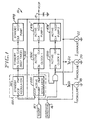
- FIG. 1 is a block diagram of an embodiment of the voltage generator according to the present invention.
- FIG 2 is a block diagram of the voltage regulator circuit 100 including standby regulator circuit 110 and active regulator circuit 200 shown in Figure 1.
- FIG 3 is a detailed schematic of standby regulator circuit 110 (shown in Figure 2) for the standby circuit.
- Figure 4 is a detailed schematic of the standby master clock circuit of the standby clock circuit for generating a standby master clock signal.
- Figure 5 is a block diagram of the clock circuit for both the standby clock and the active clock for generating clock signals for the standby pump and the active pump, respectively.
- Figure 6 is a schematic diagram of the pump circuit used for the standby pump and the active pump.
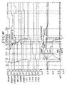
- Figure 7 is a timing diagram for the input and output signals and voltages at various nodes of the standby pump circuit.
- Figure 8 is a detailed schematic of the active regulator circuit 200 shown in Figure 2 for the active circuit.
- Figure 9 is a detailed schematic of the active master clock circuit of the active clock circuit for generating a master clock signal.
- Figure 10 is a timing diagram for the input and output signals and voltages at various nodes of the active pump circuit.
- Figure 11 is a block diagram of a second embodiment of the voltage regulator circuit having no active regulator.
- Figure 12 is a detailed schematic of the master clock circuit for the active pump for the second embodiment.
- FIG. 1 is a block diagram of a voltage generator circuit 10 according to a first embodiment of the present invention.
- the voltage generator circuit of the present invention is used for generating, controlling, and maintaining a high voltage V CCP for low power applications in an integrated circuit, such as a DRAM or other memory device.
- an integrated circuit such as a DRAM or other memory device.
- the present invention is described in reference to a DRAM by way of example, this circuit could be employed in other circuits where the voltage at a node may drop and must be maintained at a certain voltage.
- Circuit 10 produces its output voltage V CCP at an output node 12.
- Inputs 14 and 16 receive signals RASPB and 2KREFPAD, respectively. These are described infra .
- the voltage at output node 12 is used to drive word lines in an array of memory cells, for example, as represented by circuits 18 and 20 controlled by switches (e.g., decoders) S1 and S2 in Figure 1.
- switches e.g., decoders
- S1 and S2 switches
- the voltage V CCP will be low at initial power-up, as well as through leakage current.
- This voltage drop at V CCP is shown by a constant current source 22 in the block diagram of Figure 1 representing the continuous current leakage.
- a voltage regulator circuit 100 including standby regulator 110 and active regulator 200, monitors the voltage V CCP to determine whether V CCP has dropped too low.
- the standby regulator When V CCP has dropped below a desired voltage, the standby regulator activates a standby clock 300 which outputs clock signals to drive a standby pump 478. Because standby regulator 110 is constantly running, it is designed to generally draw low current to minimize power consumption in the circuit. The standby circuits react quickly enough and pump enough current to maintain V CCP at a desired voltage as a result of leakage current.
- a circuit may experience greater current loss other than merely leakage current and therefore may require an active pump.
- current is often drawn from node 12, as by operation of circuits 18 or 20, and this lowers the voltage V CCP .
- Switches S1 and S2 are closed when RASBP goes low to show the current typically drawn in a DRAM when word lines are accessed or driven. Note that the constant current sources shown in the circuit are merely representative of current loss resulting from leakage or accessing the word lines.
- a low RASBP enables active regulator circuit 200 to monitor V CCP . If V CCP is low when the word lines are accessed, then the active regulator enables the active clock 500 to generate clock signals for active pump 478'. Generally, the active regulator 200 responds more quickly than the standby regulator 110 for pumping charge to maintain V CCP when word lines are accessed. Because active regulator 200 draws more current and consumes more power, preferably it is activated only if V CCP falls or has fallen below a desired value when the word lines are accessed. In addition, active pump 478' is a larger pump (i.e. able to pump more current than the standby pump) to pump charge to maintain V CCP more quickly when the word lines are accessed. Further, the active clock circuit is a self-timed circuit and, therefore, eliminates the need for a free running oscillator. The self-timed feature will be discussed in more detail infra .
- the 2KREFPAD input 16 is included to optionally activate a second active pump 478'.
- the second active pump and associated clock circuitry is employed when a 2K refresh cycle for the DRAM is used. When a 2K refresh cycle is used, twice as many word lines are accessed, drawing more current to lower V CCP . While any number of active pumps could be used, these pumps (and related circuits) are identical. Similarly, a single active clock could drive multiple active pumps, or preferably, a separate active clock could drive each pump. Therefore, the description of active circuitry infra will refer to only one active pump and one active clock circuit.
- Regulator 100 includes a first resistor divider network 112, having resistors 113, 114 and 115 and an output node N1.
- Network 112 generates a reference signal V CCPREF , which is proportional to the voltage V CCP .
- a second resistor divider network 116 including resistors 117 and 118 and an output node N2, generates a reference voltage V CCREF , which is proportional to a power supply voltage V CC .
- the voltage divider outputs V CCREF and V CCPREF are applied to positive and negative (non-inverting and inverting) inputs respectively of a differential amplifier 120 of the standby voltage regulator 110.
- V CCREF exceeds V CCPREF
- the output of the differential amplifier 120 is high, outputting a high PUMP signal after being passed through a series of inverters 140, 150, a latch 170 and an inverter 190.
- the standby circuit is designed to limit power in the circuit, and to this end, inverters 140, 150, latch 170 and inverter 190 are included and do limit current in the circuit. The details of the inverters and latch will be described in reference to Figure 3, infra .
- Active regulator circuit 200 is also shown in Figure 2 to contrast how standby regulator circuit 110 and active regulator circuit 200 compare the reference voltages at nodes N1 and N2 to output signals to enable the standby and active clock circuits, respectively, which drive the standby and active pump circuits.
- active regulator circuit 200 receives an ENREGB signal and is enabled only under certain circumstances.
- Active regulator circuit 200 employs a differential amplifier 220 which also receives reference voltages V CCREF and V CCPREF from resistor divider networks 112 and 116.
- the active regulator circuit also includes an inverter 202 and an enabling transistor 210.
- Enabling transistor 210 is responsive to the ENREGB signal and enables or disables the differential amplifier 220 depending on whether word lines are being accessed.
- An enabling transistor is not used with differential amplifier 120 of the standby circuit which outputs a signal depending only upon the voltages at nodes N1 and N2.
- a switch 240 is also coupled to an inverter 202. Switch 240 controls whether the output of differential amplifier 220 is passed to a Schmitt trigger inverter 260 and an inverter 270 to output a PUMPA signal.
- the active regulator circuit 200 will be described in detail in reference to the active circuit.
- FIG. 3 having shown the general operation of the voltage regulator circuit 100 in Figure 2, additional features of the standby regulator circuit 110 which reduce current loss and power consumption are shown in the detailed schematic diagram.
- the preferred dimensions of the transistors in Figure 3 can be found in Appendix A, although other dimensions could be used within the scope of the invention.
- the preferred devices shown in the schematic diagrams are those well known in the art (e.g. for example, transistor 114 of Figure 3 is a P channel enhancement type transistor with the substrate coupled to the source), although other devices could be used.
- all transistors are preferably enhancement type transistors, although depletion type transistors could be used.
- the standby voltage regulator circuit 110 of Figure 3 is designed to generally operate on low current and limit current loss in the circuit.
- the resistor networks 112 and 116 include transistors configured as resistors (i.e., transistors having the gate tied to the source or drain). Because the current through the transistors is a function of the ratio of the channel width/length ratio, the channel lengths of these enhancement transistors are generally long to limit current through the transistor networks.
- capacitors 111 and 119 can be added at nodes N1 and N2 respectively to cause the voltage at the nodes to change more rapidly.
- capacitor 111a is 2pf and capacitor 111b is 1pf.
- Capacitors 119 are preferably 1pf.
- the transistors are preferably formed using metal and oxide layers on the device, transistors configured as capacitors could be used.
- the differential amplifier circuit 120 preferably consists of a conventional configuration of transistors 122-128 and is used to compare V CCREF at a node N2 with V CCPREF at a node N1 to output a PUMP signal.
- the preferred dimensions of the transistors 122-128 (shown in Appendix A) of the differential amplifier circuit 120 are specifically chosen to keep current in the circuit low, and therefore minimize power consumption.
- the width/length ratio of the transistors of the differential amplifier circuit 120 is preferably kept small by selecting long channel lengths to limit the current flow.
- a slow changing signal can often lead to current loss in a circuit, particularly when input to a two transistor inverter. Specifically, both transistors of the inverter will be on for a certain period of time, leading to "through current” or “crowbar current” through the series of transistors. Therefore, there is often current loss from V CC to ground by way of a two transistor inverter during the transition.
- transistors 130-136 are added to differential amplifier circuit 120.
- the sources of transistors 130 and 132 are coupled together at V CC , while the drains of transistors 130 and 132 are also coupled together to transistor 122.
- the gate electrode of transistors 130 and 132 are coupled together and are coupled to the gates of transistors 122, 124 and 134.
- the sources of transistors 134 and 136 are coupled together at V CC , while the drains of transistor 134 and 136 are coupled together at transistor 124.
- the gate of transistor 136 is coupled to the output of the differential amplifier 120.
- Transistors 130-136 are added to drive the output more quickly without drawing additional current. Particularly, these transistors drive the output V OUT at node N3 of the differential amplifier circuit 120 when output V OUT is at a transition point (i.e. a point between outputting a high and low signal).
- transistor 126 begins to turn on harder, pulling node N3 low. Since node N3 is coupled to the gate of transistor 136, which is a p channel FET, it begins to turn on harder. Its source-drain path couples VCC to the source of transistor 124, which now reaches a higher potential and, therefore, turns on transistor 124 harder. This raises the potential at the drain of FET 124 and the gate electrodes of transistors 122, 130, and 132. This permits the output at node N3 to be pulled low even more quickly.
- circuit 120 acts to drive the output at node N3 high quickly as V CCPREF (node N1) begins to drop below V CCREF (node N2). Specifically, as V CCPREF begins to drop, FET 126 becomes less conductive, permitting the voltage at node N3 to begin to rise. When this happens, p channel transistor 136 becomes less conductive, which lowers the voltage at the source of transistor 124. As a result, the voltage at the drain of transistor 124 is lowered, turning on transistor 122, 130, and 132 harder and driving the output at node N3 high more quickly.
- inverters 140 and 160 and latch 170 are specifically designed to reduce the "through current" in the inverters and to output a PUMP signal (i.e. clock enabling signal) having a sharp transition.
- the switching time of transistors is generally dependent on the channel width/length ratio. Therefore, the channel widths and lengths can be chosen to establish when the transistors of the inverters will switch. Because the widths of the transistors in inverter circuit 140 are the same, the switching time will be a function of their channel lengths.
- the channel lengths of the transistors 144, 146, 156 and 158 of circuit 140 are chosen so that the voltages at nodes N4 and N5 (and therefore transistors 162 and 164 of circuit 160) switch at an appropriate time.
- the width/length ratios of the transistors of inverter 140 are selectively chosen. Specifically, the width/length ratio of transistor 144 is generally greater than that of transistor 156. As a result, transistor 144 turns on before transistor 156 turns on. Therefore, node N4 is pulled high before node N5 is pulled high to ensure that transistor 162 switches before transistor 164.
- the width/length of transistors 146 and 158 are selectively chosen. Specifically, the width/length ratio of transistor 158 is generally greater than that of transistor 146. As a result, transistor 158 turns on before transistor 146 turns on. Therefore, node N5 is pulled low before node N4 is pulled low to ensure that transistor 164 turns off before transistor 162 turns on. Accordingly, the selection of channel lengths of the transistors of inverter circuit 140 reduces any current path from V CC to ground in inverter 160 during either transition.
- transistors 148 and 154 are added to inverter 140 to eliminate any through current in inverters 143 and 153. Because of the "current-limiting" transistors 148 and 154 have long channel lengths, nodes N4 and N5 will not be pulled rapidly to ground and V CC respectively. Therefore, a path from V CC to ground will exist while driving transistors 162 and 164, but the current will be reduced in the series of transistors 144-148 and 154-158 by the long channel lengths of transistors 148 and 154. Also, transistors 148 and 154 are selectively positioned to ensure that the timing of the switching of the transistors as described above is not affected.
- transistor 148 While “current-limiting" transistor 148 does effect the timing of driving node N4 low when node N3 transitions from low to high, the capacitive coupling of transistor 148 to node N4 is large enough to pull node N4 low enough to turn on transistor 162 at an appropriate time.
- inverter 153 drive node N5 low very quickly by turning on transistor 158 to shut off transistor 164.
- the "current-limiting" transistor 154 is added only to the p-channel side of inverter 153 to limit the effect of transistor 154 on transistor 158.
- a current limiting transistor is not added in series between transistor 158 and ground in order to avoid limiting the rate at which transistor 158 pulls N5 to ground.
- "current-limiting" transistor 154 does affect the timing of driving node N5 high when node N3 transitions from high to low, the capacitive coupling of transistor 154 to node N5 is large enough to pull node N5 high enough to turn on transistor 164 at an appropriate time.
- the standby regulator circuit 110 includes a latch 170 to maintain the output of the PUMP signal during the period when neither transistor 162 nor transistor 164 of inverter 160 is on (as discussed above to prevent through current).
- the inverted PUMP signal is fed back via line 185 to transistor network 174-180 to maintain the original voltage at node N6 until the state of N6 changes when invertor 160 drives node N6.
- latch 170 itself is designed to limit the through current while also providing a weak latch.
- Transistors 162 and 164 are generally small transistors (i.e., small widths and lengths) to limit the current required from inverter 140 to switch inverter 160.
- they because of their size, they generally cannot drive a large capacitive load at node N6. Too large a capacitance at node N6 is undesirable because this capacitance will cause the voltage at the node to switch slowly. Therefore, a weak latch is provided at node N6 by selecting transistors 174 and 176 to have smaller widths and lengths, preferably on the order of 1-2 ⁇ m, to limit the capacitance.
- transistors 174 and 176 of the latch have widths and lengths which are about equal, they also have a large width/length ratio and drive greater current. Therefore, "current-limiting" transistors 178 and 180 are included. These transistors have long channel lengths (and therefore small width/length ratios) to limit the current in the latch 170 and reduce power consumption in the circuit.
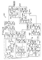
- the master clock circuit 301 for the standby clock 300 is shown in Figure 4.
- Circuit 301 receives the PUMP signal at an input and produces a master clock output signal MCLKS.
- MCLKS master clock output signal
- the pump circuit pumps on a two-cycle principle: a precharge cycle and a pumping cycle. Therefore, the clock circuit must generate different signals during these cycles. The clock signals generated during the pumping cycle will be described first, followed by the clock signals generated during the precharge cycle.
- the standby master clock circuit 301 of Figure 4 which generates the master clock signal MCLKS for the standby circuit will be described first, followed by the operation of a clock circuit 445 shown in Figure 5.
- the standby regulator 110 when the constantly running standby regulator 110 ( Figure 3) detects that V CCPREF has fallen below a selected value, the standby regulator will output a high PUMP signal.
- a high PUMP signal drives the gate of transistor 312 high.
- FET 314 is on, so that when FET 312 turns on, it pulls the gates of transistors 304 and 306 low.
- Transistors 304 and 306 form an inverter having an output node "START,” which thus is pulled high.
- the output MCLKS of master clock circuit 301 is high after START is transmitted through a sequence of inverters 316 and 322.
- a high pump signal and MCLKS signal are generated by the circuits to drive the charge pump, the circuits could be configured to generate active low pump and MCLKS signals within the scope of the present invention.
- MCLKS varies during the different cycles. Therefore, the feedback operation of standby master clock circuit 301 designed to change the MCLKS signal (i.e., between a binary low and binary high signal) will be described first, followed by a description of the clock circuit 445 which receives the MCLKS signal.
- MCLKS While the pumping cycle is completed when MCLKS is high, MCLKS is fed back through circuit 301 of Figure 4 to generate a low MCLKS during the precharge cycle to reset the inputs and voltages at the nodes of the pump circuit for the next pumping cycle.
- MCLKS signal After passing through inverters 328 and 334, MCLKS signal follows two paths. Two paths are designed to establish the proper voltages at node START for the precharge and pumping cycles. Depending on the state of MCLKS, MCLKS signal generally will be transmitted through the circuit quickly in one of the paths, while a delay will be provided in the other path. Generally, a first path exists through an inverter 342, a delay circuit 350, and gates 370, 380 and 390.
- a second path is provided by a delay circuit 400 (having inputs at the gate electrodes of transistors 404 and 412) and inverter 430 and 440. Because the signal from the fast path (i.e. either the first or second path, depending upon the state of MCLKS) reaches a latch 302 first and, therefore, establishes a condition of the latch, the fast path will be discussed first, followed by the slow path.
- inverter 342 When MCLKS is high (for example, during the pumping cycle), the signal is passed through inverters 328 and 334 and a high signal is input to inverter 342. The output of inverter 342 is low, turning on a transistor 354 and turning off a transistor 352. Because there is no path from a node N1 to ground through transistors 352 and 360, capacitor 364 is pulled to V CC via the source-drain path of FET 354. As a result, capacitor 364 charges quickly, providing the fast path through the circuit to latch 302. Specifically, the voltage at node N1 is transmitted through Schmitt Trigger inverter 370 and inverters 380 and 390 to output a low signal at the gate of a transistor 314, turning it off. With transistor 314 off, the circuit ignores the PUMP signal at the gate of transistor 312, providing the self-timed feature of the circuit. Accordingly, an oscillator is not needed to provide timing for the clock circuit.
- inverter 334 is input to delay circuit 400 (which provides the slow path of the circuit in this case). Because the output of inverter 334 is high, transistor 404 is off and transistor 412 is on. Therefore, a path from a capacitor 402 through transistor 406 and resistor 410 is provided to ground, leading to the discharge of capacitor 402. Because capacitor 402 is relatively large, preferably 1.2 pf, and resistor 410 is also large, preferably 10K ⁇ , this discharge of the capacitor provides a long delay (preferably 40-60 nanoseconds). The delay provided by discharging the capacitor is established to ensure the pump circuit 478 completes the pumping cycle (described in detail in reference to the pump circuit).
- the voltage at node N2 of the capacitor 402 is input to a Schmitt Trigger inverter 420 and inverters 430 and 440 to provide an output to the gate of a transistor 450.
- the high output at the gate of the n-channel transistor 450 turns it on, thereby pulling the node START to ground and inverting the latch 302.
- the low voltage at the node START is transferred through inverters 316 and 322 to provide a low MCLKS output signal which starts the precharge cycle of the pumping circuit to prepare the circuit for the next pumping cycle.
- MCLKS When master clock MCLKS is low, MCLKS is passed through inverters 328 and 334, providing a low output of inverter 334.
- the output of inverter 342 is high, turning off transistor 354 and turning on transistor 352. Because a path from capacitor 364 to ground is provided by way of transistors 360 and 352, allowing for the discharge of capacitor 364 (i.e., node N1), the delay through delay circuit 350 is long, while the delay through delay circuit 400 is short. Therefore, the passage of the low MCLKS through delay circuit 350 will be described after the short path through delay circuit 400.
- the low output signal of inverter 334 is input to transistors 404 and 412 of delay circuit 400.
- the low signal turns on transistor 404 and turns off transistor 412. Therefore, the capacitor 402 is coupled to V CC via transistor 404 and the capacitor charges quickly, pulling the voltage at node N2 high.
- the voltage at node N2 is transmitted through Schmitt trigger inverter 420 and inverters 430 and 440.
- a low output of inverter 440 is input to transistor 450.
- the low signal at the gate of transistor 450 turns off the transistor and allows the pumping cycle to begin again after the signal passes through the slow path (i.e., delay circuit 350) and the circuit receives an active pump signal to reset latch 302.
- the discharge of capacitor 364 generally provides a delay.
- the low output of inverter 334 is input to inverter 342.
- the output of inventer 342 is input to delay circuit 350.
- the high input turns on transistor 352 and turns off transistor 354.
- a path is provided from capacitor 364 to ground by way of transistor 360, a resistor 362 (preferably 10K ⁇ ) and transistor 352.
- a transistor 356 and resistor 358 are added to maintain a constant current in the path from node N1 to ground and, therefore, establish a set delay.
- the inputs to the pump circuit and voltages at various nodes of the pump are reset for a subsequent precharge and pumping cycle.
- This delay for the precharge cycle (set by delay circuit 350) is generally shorter than the delay for the pumping cycle (set by delay circuit 400) by providing a smaller capacitor which is discharged.
- a long delay during the precharge cycle is not required because the internal voltages in the pump reach precharge levels more quickly. This is because the gate-to-source voltages are higher and can react or provide more current at a faster rate.
- the standby master clock circuit 301 shown in Figure 4 is responsive to an active PUMP signal (or clock enabling signal from the standby regulator circuit shown in Figure 3 when V CCPREF drops below a certain value) and generates the MCLKS signal.
- MCLKS is fed back through the circuit and varies during different cycles.
- MCLKS is input to the clock circuit 445 shown in Figure 5. As MCLKS transitions high or low, clock circuit 445 generates different clock signals during the different cycles to drive the charge pump.
- clock circuit 445 receives MCLKS at an input and outputs signals CP1 through CP5. This circuit shows the preferred configuration of gates to generate the signals to drive the charge pump in Figure 6.
- the signals generated by clock circuit 445 are shown in the timing diagram of Figure 7.
- Clock circuit 445 uses a series of gates and feedback paths to generate the outputs shown in the timing diagram of Figure 7.
- the operation of each gate shown in Figure 5 is well known in the art.
- each signal is a part of a feedback loop to provide an inverted output depending on the status of the signals. As a result, the outputs transition based upon state of the master clock signal as well as the previous signal.
- the configuration of the gates is designed to establish the signals shown in Figure 7.
- One skilled in the art could follow the MCLKS input signal to generate the output signals in Figure 7 at any period based upon the previous input signals. While the preferred clock circuit is shown in Figure 7, any other circuit or other means of generating signals (CP1-CP4) shown in Figure 7 could be used within the scope of the present invention to generate the input signals to the pump circuits.
- Pump 478 receives at several inputs the clock signals CP1 through CP5, and provides an output V CCP . While the operation of the pump is shown having a 2.7 volt V CC , some other value of V CC could be used. The use of a 2.7 volt V CC is simply illustrative.
- the charge pump of the present invention is a hybrid two-stage charge pump having a first stage 477. Charge pumped to a node N4 during the first stage of a pump cycle (by first stage 477) is used to enable the charge pump to pump charge from a node N1 to V CCP during a second stage of the pumping cycle.
- signal CP1 is used to drive nodes N1 and N2 to a greater potential by way of capacitors 479 and 480.
- Signals CP2, CP3, CP4 and CP5 are generally used to regulate the operation of the remaining transistors in the circuit to pump charge to V CCP during the pumping cycle, and to reset the nodes during the precharge cycle. Further details of the charge pump are disclosed in copending European Application No. 93202505.9 filed on August 26, 1993, the entire specification of which is incorporated herein by reference.
- the input signal to the pump circuit and the voltages at various nodes are shown at t0 when the pump circuit is in a quiescent state.
- the input signals CP1 to CP5 are established by the clock circuit 445 shown in Figure 5, while the voltage at the nodes of the pump circuit in Figure 6 are determined by the clock signals CP1-CP5.
- CP2 is high (V CC ), turning on transistors 486 and 491 to maintain nodes N1 and N2 at V CC .
- PUMP signal goes high (after the standby voltage regular circuit 110 shown in Figure 3 detects a drop in V CCP ).
- MCLKS signal also goes high.
- CP2 goes low (0 volts), turning off transistors 486 and 491 to prevent any transfer of charge from node N1 by way of transistor 486 to V CC and to prevent any transfer of charge from node N2 by way of transistor 491 to V CC .
- CP4 also goes high to turn on transistor 490 and to allow transfer of charge from N2 to N4 (when CP1 goes high at t2).
- CP5 goes low to turn off transistor 488 and unclamp node N4 from V CC .
- CP1 goes high, driving the voltage at nodes N1 and N2 to approximately 2V CC (or 5.4 volts for a 2.7 volt V CC ). Because transistor 490 is on, node N4 approaches 2V CC (or approximately 2V CC minus V t or 3V CC /2). This transfer of charge is necessary to turn on transistor 489 at a time t4.
- CP4 goes low to turn off transistor 490 and to end the first stage of the pumping cycle of node N4 by preventing a transfer of charge from node N4 to node N2.
- CP3 goes high to start the second stage of the pumping cycle.
- a high CP3 signal turns on transistor 489 to allow the transfer of charge from node N1 to V CCP .
- the charge at node N1 and V CCP begin to equalize.
- the pump signal may or may not go low (as shown by the dotted line), depending on whether V CCP has been restored to its desired value.
- the dashed line designating a high pump signal is shown in Figure 7 and will be discussed further in regard to the end of the precharge cycle (at time t10).
- the pumping cycle is complete as the high MCLKS signal is fed back through the master clock circuit 301 (discussed in Figure 4). As MCLKS goes low, CP3 goes low to end the pump cycle.
- the pump must then reset the inputs (CP1-CP5) and the voltages at the nodes (N1-N5) to their quiescent values for the next precharge and pumping cycle.
- CP5 transitions high to couple node N4 to V CC .
- CP1 transitions low to drive nodes N1 and N2 to V CC .
- CP2 goes high to couple nodes N1 and N2 to V CC and maintain the voltage at the node.
- MCLKS has passed through master clock circuit 301 to turn on transistor 314 to receive a pump signal. If enough charge had not been pumped as of t5 (i.e., the PUMP signal had not gone low as indicated by the dashed line), pumping would begin at time t10 as MCLKS goes high (as shown in the dashed line). The precharge cycle would again begin as shown at time t1. Otherwise, the circuit remains in a quiescent state until a time t11, when V CCP has again dropped and an active PUMP signal is generated by the standby regulator 110 to begin the pumping cycle again.
- the standby circuit of the present invention monitors V CCP and activates the standby charge pump to maintain a desired voltage at V CCP .
- the standby regulator circuit, clock circuit and standby pump are designed to consume low power. Specifically, only the standby regulator circuit is constantly operating to monitor V CCP and is specifically designed to minimize power consumption.
- the clock circuit and pump circuits are enabled and draw current only when V CCP has dropped below a desired value, due typically to leakage current or initial power up.
- active circuit 500 includes active regulator 200 (Figure 8), active master clock 501 (Figure 9), clock circuit 445 ( Figure 5) and pump circuit 478' ( Figure 6).
- active circuits operate independently of (although simultaneously with) the standby circuits and are enabled when the word lines of a DRAM are accessed, as indicated by a RASBP signal. If V CCP drops below a desired value when the word lines are accessed and the active circuit is enabled, the active pump (which is generally a larger pump than the standby pump) will pump charge to V CCP to maintain the desired voltage at V CCP .
- active regulator circuit 200 also regulates the voltages V CCPREF and V CCREF at nodes N1 and N2, respectively, to determine if V CCP has fallen below a desired value.
- the active regulator 200 also receives an ENREGB signal, which enables or disables the active regulator circuit 200.
- the state of ENREGB signal is determined, for example, by whether the word lines of a DRAM are driven and, therefore, the circuit is drawing current which lowers V CCP .
- a low ENREGB signal is inverted by inverter 202 and drives the gate of transistor 210 to enable differential amplifier 220.
- Differential amplifier 220 includes the conventional configuration of transistors 222-228. The operation of the differential amplifier is well known in the art. However, the differential amplifier further includes transistors 232 and 234 to enable the amplifier to respond more quickly to provide an output at V OUT .
- Transistors 232 and 234 generally serve the same functions as transistors 130 to 136 of standby differential amplifier 120 (Fig. 3). However, because long channel transistors are not used in this differential amplifier (unlike those of the standby differential amplifier 120) to limit current, the capacitance at the output node V OUT is not as great. Therefore, transistors 232 and 234 could be coupled in parallel to transistors 222 and 224, respectively, to more quickly drive the output without increasing the capacitance at the output node V OUT.
- a switch 240 is also responsive to the ENREGB signal to allow the output of the differential amplifier 220 to be output as a PUMPA signal (similar to the PUMP signal of the standby master clock circuit).
- a low ENREGB signal is twice inverted by inverters 202 and 241, so node N7 is also low and is coupled to the gate of transistor 208, turning off the transistor.
- the low output of inverter 241 is inputted to inverter 249 and is also applied to the gate of transistor 252, which turns on.
- the output of inverter 249 turns on transistor 250, providing a path from the output of the differential amplifier (V OUT ) to the output at PUMPA by way of inverters 260 and 270.
- the output V OUT of differential amplifier 220 is transmitted through the switch 240 to node N8.
- Node N8 is coupled to a Schmitt trigger inverter 260, the output of which is inverted by an inverter 270 to provide the output signal PUMPA.
- the PUMPA signal is used by the active master clock circuit 501 (shown in Figure 9) to generate a MCLK signal.
- the active master clock circuit 500 outputs a high MCLK signal when an input RASBP is low and an input PUMPL (i.e. PUMPA previously latched as PUMPL) is high.
- a high RASBP drives ENREGB low which enables the active voltage regulator described supra in Figure 8 to monitor V CCP . If V CCP has dropped below a desired value, the active voltage regulator will output an active PUMPA signal (which is input to the active master clock circuit 501 of Figure 9).
- PUMPL is high
- MCLK is high to enable a clock circuit to drive the pump circuit.
- the same clock circuit 445 shown in Figure 5 is used to generate clock signals CP1-CP5 to drive the active pump circuit 478'.
- the active pump circuit 478' is identical in structure to the standby pump circuit.
- transistors having different channel widths and lengths are used in the active pump circuit to drive more current to maintain the voltage at V CCP .
- the preferred values of the channel lengths and widths of corresponding transistors employed in the active pump are shown in parenthesis in Appendix A.
- clock circuit 445 and the active pump circuit 478' are identical to that of the standby circuit.
- clock circuit 445 is responsive to the MCLK signal (similar to MCLKS of the standby master clock circuit 301) to generate clock signals to operate the active pump circuit 478'.
- MCLK signal similar to MCLKS of the standby master clock circuit 301
- the relationship of the MCLK signal to the clock circuit 445 and the active pump circuit 478' has been described in detail in reference to the standby circuit and will not be repeated here. Therefore, only the role of the RASBP signal (indicating that the word lines of a DRAM are being accessed) and other signals in the active master clock circuit 501 to generate a MCLK signal will be discussed in detail.
- active master clock circuit 501 of Figure 9 The detailed operation of active master clock circuit 501 of Figure 9 is now described. Because RASBP can be either high or low (indicating whether the word lines of a DRAM are being accessed and the active pump should be activated if V CCP drops below a given value), the operation of the circuit will be described separately in both states.
- delay circuit 502 provides a low RASBPP at node N2 after a small delay.
- RASBPP is a signal which remains low for an additional period of time longer than RASBP, as will be explained infra .
- a transistor 506 is turned off, decoupling the path from a current source 509 to ground.
- a low RASBP signal also turns on a transistor 504, which couples a node N1 to V CC . Because FET 504 presents little resistance between node N1 and V CC , capacitor 508 charges almost immediately and node N1 transitions quickly to V CC . This high state at node N1 provides a low RASBPP after passing through a sequence of inverters 520, 530 and 536.
- RASBPP signal is input to a number of circuits which control the output MCLK.
- the timing of the circuit will be understood in reference to the diagram of Figure 10.
- a constant current source is used to discharge a capacitor to set a delay, although other means of setting the delay could be used.
- transistor 546 of the delay circuit 540 when the RASBPP signal transitions from high to low, transistor 546 of the delay circuit 540 is turned off, decoupling the path from current source 549 to ground. Also, transistor 544 is turned on, coupling the capacitor 548 at node N3 to V CC . This capacitor charges quickly, providing a high output at node N3 to inverters 560 and 570.
- inverter 570 and signal RASBPP are input to a NAND gate 580 at nodes N4 and N5 respectively.
- the output of the NAND gate (NAND OUT) is therefore high.
- This high output of the NAND gate provides a high ENREGB signal after NAND OUT passes through inverters 590 and 596. Therefore, when RASBP is low, active master clock circuit 500 disables the active voltage regulator circuit 200 (shown in Figure 8) and regulator 200 then no longer monitors V CCP or transmits a high PUMPA signal if V CCP has dropped below a desired value.
- NAND OUT The output (NAND OUT) of NAND gate 580 also coupled to a switch 600.
- This switch generally allows the PUMPA input signal to be latched by latch 610 (as PUMPL).
- Inverters 590 and 596 are coupled to the output of NAND gate 580 to add a short delay to ensure that switch 600 is disabled before ENREGB goes high to disable the voltage regulator circuit. This ensures that the correct PUMPA signal is latched.
- Latch circuit 610 is coupled to an inverter 620, the output of which is a signal PUMPL.
- switch 600 prevents the PUMPA signal from being transferred to transistor 626. Therefore the value of PUMPL will be determined by the previously latched PUMPA signal (i.e. when RASBPP was previously high).
- PUMPL is input to a transistor 626.
- the latch 630 will be allowed to receive PUMPL when transistor 640 is turned on by a low RASBPP signal passed through inverter 642. When RASBPP is low, transistor 648 is turned off and the output of latch 630 is determined by PUMPL.
- the output of latch 630 is passed through inverters 650 and 660 to generate the output signal MCLK. If PUMPL is high and RASBPP low, the START signal will be high, which is output through inverters 650 and 660 to provide a high MCLK. If PUMPL is low, the START signal will be low to provide a low MCLK.
- active master clock 501 will be described as RASBP transitions from low to high at time t5.
- transistor 504 is turned off and transistor 506 is turned on. Therefore, capacitor 508 discharges to ground through constant current source 509. Therefore, a delay is provided (designated as delay 3 in Figure 10). As stated earlier, this delay is to ensure that the pumping circuit 478' remains in the pumping cycle for a sufficient time to adequately pump V CCP to a desired voltage.
- the low signal at node N1 is transmitted through inverters 520, 530 and 536.
- the output of inverter 536 provides a high RASBPP signal at a time t6 after capacitor 508 is discharged (i.e. after delay 3).
- the high RASBPP signal is input to delay circuit 540.
- the high signal turns off transistor 544 and turns on transistor 546, providing a path from capacitor 548 at node N3 to ground by way of current source 549.
- RASBPP is high while the output of inverter 570 is high.
- Both RASBPP and the output of inverter 570 are input to NAND 580.
- the output (NAND OUT) of the NAND gate is low, opening switch 600 and providing a low ENREGB.
- the output of inverter 570 is low, driving the output of the NAND gate (and ENREGB) high.
- This delay (designated as delay 4 in Figure 10) is provided to ensure that ENREGB remains low for a predetermined time for the voltage regulator circuit to compare V CCPREF with V CCREF to determine whether to pump on the next cycle where RASBP goes low. Also, as stated earlier, inverters 590 and 596 are added to the output of the NAND gate 580 to ensure that ENREGB stays low when switch 600 is closed (i.e. when the output NAND OUT of the NAND gate 580 goes low) to ensure that the correct PUMPA signal is latched by latch 610 when RASBP is high.
- the high RASBPP signal generates the ENREGB signal to determine whether to pump when RASBP goes low
- the high RASBPP also generates a low MCLK signal (at time t7 in Figure 10).
- the latch 630 will be allowed to receive PUMPL only when transistor 640 is turned on by a low RASBPP signal passed through inverter 642. Because RASBPP is high, the output of inverter 642 is low, turning off transistor 640 to ignore the PUMPL signal, providing a self-timing clock which eliminates the requirement for an oscillator.
- the gate of transistor 648 is high, turning on the transistor to drive the START node low and to generate a low MCLKS signal.
- the active regulator circuit can be eliminated as shown in the block diagram of Figure 11 and the charge pump can pump whenever RASBP goes low.
- the master clock circuit 501 Like circuit components in Figure 12 are numbered the same as those in Figure 9.
- the primary difference in the circuit is that the circuit does not require an active regulator. Rather, a pump signal (i.e. PUMPA or PUMPL) is pinned at V CC and the output MCLK of this master clock circuit is high whenever RASBP goes low.
- PUMPA or PUMPL a pump signal
- the operation of this circuit is identical to the circuit in Figure 9, excluding any requirement to generate a PUMPA signal, a PUMPL signal and an ENREGB signal, and therefore, is not described again in detail here.
Landscapes
- Engineering & Computer Science (AREA)
- Power Engineering (AREA)
- Physics & Mathematics (AREA)
- Microelectronics & Electronic Packaging (AREA)
- Electromagnetism (AREA)
- General Physics & Mathematics (AREA)
- Radar, Positioning & Navigation (AREA)
- Automation & Control Theory (AREA)
- Nonlinear Science (AREA)
- Dram (AREA)
- Dc-Dc Converters (AREA)
Claims (23)
- Verfahren zum Aufrechterhalten einer Spannung, welche größer als eine Energieversorgungsspannung (VCCP) ist, in einer die Energieversorgungsspannung empfangenden integrierten Schaltspeichervorrichtung, wobei das Verfahren die folgenden Schritte umfaßt:kontinuierliches Überwachen der Spannung, welche größer als die Energieversorgungsspannung (VCCP) ist, auf einen Spannungsabfall;Erzeugen erster Taktgebersignale (CP1-CP5) als Reaktion auf die Entdeckung eines Abfalls in der Spannung, welche größer als die Energieversorgungsspannung (VCCP) ist, während des Schritts des kontinuierlichen Überwachens;Betätigen einer ersten Ladungspumpe (478) als Reaktion auf die ersten Taktgebersignale (CP1-CP5) und Anlegen von Ladung daraus mit derselben Polarität wie die Energieversorgungsspannung an einen kapazitiven Knoten (12) zwecks Antreibens von Wortleitungen in einer Anordnung von Speicherzellen;diskontinuierliches Überwachen der Spannung, welche größer als die Energieversorgungsspannung (VCCP) ist, auf einen Spannungsabfall, wobei der Schritt des diskontinuierlichen Überwachens der Spannung, welche größer als die Energieversorgungsspannung (VCCP) ist, unabhängig vom Schritt des kontinuierlichen Überwachens der Spannung, welche größer als die Energieversorgungsspannung (VCCP) ist, immer dann durchgeführt wird, wenn eine Wortleitung der Speichervorrichtung angetrieben wird;Erzeugen zweiter Taktgebersignale (CP1-CP5) als Reaktion auf die Entdeckung eines Abfalls in der Spannung, welche größer als die Energieversorgungsspannung (VCCP) ist, während des Schritts des diskontinuierlichen Überwachens;Betätigen einer zweiten Ladungspumpe (478') als Reaktion auf die zweiten Taktgebersignale und Anlegen von Ladung daraus mit derselben Polarität wie die Energieversorgungsspannung an den kapazitiven Knoten (12);wobei zumindest einer dieser Erzeugungsschritte die Erzeugung eines vollständigen Zyklus von Taktgebersignalen zum Pumpen von Ladung aus der entsprechenden Ladungspumpe (478; 478') und zum Voraufladen der entsprechenden Ladungspumpe nach dem Starten dieses Erzeugungsschrittes beinhaltet, ungeachtet des Überwachens eines Abfalls in der Spannung, welche größer als die Energieversorgungsspannung (VCCP) ist.
- Verfahren zum Aufrechterhalten einer Spannung, welche größer als die Energieversorgungsspannung (VCCP) ist, in einer Speichervorrichtung nach Anspruch 1, worin der Schritt des kontinuierlichen Überwachens durchgeführt wird mittels einer Standby-Schaltung, enthaltend einen Standby-Spannungsregulator (110), der gekoppelt ist zum Überwachen der Spannung, welche größer als die Energieversorgungsspannung ist, und zum Ausgeben eines Standby-Taktgeberfreigabesignals (PUMP), wenn die Spannung von einem vorbestimmten Pegel abweicht, einer auf das Standby-Taktgeberfreigabesignal (PUMP) ansprechenden ersten Standby-Taktgeberschaltung (300) zum Erzeugen der Standby-Taktgebersignale (CP1-CP5) und der ersten Ladungspumpe, welche eine auf die Standby-Taktgebersignale (CP1-CP5) ansprechende Standby-Pumpenschaltung (478) ist, zum Pumpen von Ladung zwecks Änderung der Spannung, welche größer als die Energieversorgungsspannung (VCCP) ist.
- Verfahren zum Aufrechterhalten einer Spannung, welche größer als die Energieversorgungsspannung (VCCP) ist, in einer Speichervorrichtung nach Anspruch 1, worin der Schritt des diskontinuierlichen Überwachens der Spannung, welche größer als die Energieversorgungsspannung (VCCP) ist, durchgeführt wird mittels einer aktiven Schaltung, enthaltend einen aktiven Spannungsregulator (200), welcher gekoppelt ist zum überwachen der Spannung, welche größer als die Energieversorgungsspannung (VCCP) ist, und enthaltend einen ersten Eingang (14) zwecks Empfangs des Freigabesignals (RASBP), wobei der aktive Spannungsregulator (200) ein aktives Taktgeberfreigabesignal (PUMPA) ausgibt, wenn er durch das Freigabesignal (RASBP) freigegeben worden ist und wenn die Spannung, welche größer als die Energieversorgungsspannung (VCCP) ist, von einem vorbestimmten Pegel abweicht, zumindest einer auf das aktive Taktgeberfreigabesignal (PUMPA) ansprechenden zweiten aktiven Taktgeberschaltung (500) zum Erzeugen der aktiven Taktgebersignale (CP1-CP5) und der zweiten Ladungspumpe, welche zumindest eine auf die aktiven Taktgebersignale (CP1-CP5) ansprechende aktive Pumpenschaltung (478') ist, zum Pumpen von Ladung zwecks Änderung der Spannung, welche größer als die Energieversorgungsspannung (VCCP) ist.
- Verfahren zum Aufrechterhalten einer Spannung, welche größer als die Energieversorgungsspannung (VCCP) ist, in einer Speichervorrichtung nach Anspruch 1, worin der Schritt des diskontinuierlichen Überwachens der Spannung, welche größer als die Energieversorgungsspannung (VCCP) ist, durchgeführt wird mittels einer aktiven Schaltung, enthaltend zumindest eine auf ein Freigabesignal (PUMPA) ansprechende zweite aktive Taktgeberschaltung (500) zum Erzeugen der aktiven Taktgebersignale (CP1-CP5), und der zweiten Ladungspumpe, welche zumindest eine auf die aktiven Taktgebersignale (CP1-CP5) ansprechende aktive Pumpenschaltung (478') ist, zum Pumpen von Ladung zwecks Änderung der Spannung, welche größer als die Energieversorgungsspannung (VCCP) ist.
- Verfahren nach Anspruch 1, worin die integrierte Schaltung ein dynamischer Speicher mit Energieerhöhungs-, aktivem und Standby-Modus ist;worin der Schritt des kontinuierlichen Überwachens die Betätigung einer Niederleistungsregulatorschaltung (10), welche zu allen Zeiten aktiv ist, in denen der Speicher mit Energie versorgt wird, beinhaltet;worin der Schritt des Betätigens der ersten Ladungspumpe (478) die Spannung, welche größer als eine Energieversorgungsspannung ist, zum kapazitiven Knoten (12) liefert, wenn der Speicher hochfährt und sich im Speicher-Standby-Modus befindet;worin der Schritt des Betätigens der zweiten Ladungspumpe (478') die Spannung, welche größer als eine Energieversorgungsspannung ist, zum kapazitiven Knoten (12) liefert, wenn sich der Speicher im aktiven Modus befindet;worin das Verfahren zur Erzeugung einer Spannung, welche größer als eine Energieversorgungsspannung ist, weiters das selektive Anlegen eines ersten Freigabesteuersignals (RASBP) an einen zweiten Regulator (200) und das Überwachen der Spannung, welche größer als eine Energieversorgungsspannung ist, mit dem zweiten Regulator (200) nach Empfang des ersten Freigabesteuersignals umfaßt;worin der Schritt des Erzeugens zweiter Taktgebersignale die Lieferung eines Aktivierungssignals vom zweiten Regulator (200) an eine zweite Taktgeberschaltung (500) beinhaltet.
- Verfahren nach Anspruch 5, worin beide Schritte des Erzeugens von Taktgebersignalen das Selbsttakten der Erzeugung jeweils vollständiger Taktgeberimpuls-Zyklen trotz einer etwaigen Beendigung der entsprechenden Aktivierungssignale beinhalten.
- Verfahren nach Anspruch 6, worin das Betätigen der zumindest einen Selbsttaktgeberschaltung (300) folgendes umfaßt:das gezielte Einstellen eines Verriegelungsteils (302) auf einen ausgewählten ersten oder zweiten Zustand, wobei der erste Zustand der Erzeugung von Taktgebersignalen für das Pumpen von Ladung und der zweite Zustand der Erzeugung von Taktgebersignalen für das Voraufladen der entsprechenden Ladungspumpe (478) entspricht, unddas Blockieren des Einstellens des Verriegelungsteils (302) auf den ersten Zustand trotz des Zustands irgendeines entsprechenden Aktivierungssignals oder Freigabesignals, bis ein vollständiger Zyklus von Pump- und Vorauflade-Taktgebersignalen erzeugt ist.
- Verfahren nach Anspruch 7, worin das Betätigen der zumindest einen Selbsttaktgeberschaltung (300) weiters umfaßt:als Reaktion auf das Einstellen des Verriegelungsteils (302) auf den ersten Zustand das Erzeugen einer ersten Mehrzahl von Taktgebersignalen zum Pumpen der Ladungspumpe (478) über ein erstes Selbsttaktintervall;das Erzeugen eines ersten internen Steuersignals am Ende des ersten Selbsttaktintervalls;das Verwenden des ersten internen Steuersignals zur Einstellung des Verriegelungsteils (302) auf den zweiten Zustand;als Reaktion auf den auf den zweiten Zustand eingestellten Verriegelungsteil (302) das Erzeugen einer zweiten Mehrzahl von Taktgebersignalen zum Voraufladen der Ladungspumpe (478) über ein zweites Selbsttaktintervall;das Erzeugen eines zweiten Intervallsteuersignals am Ende des zweiten Selbsttaktintervalls;und danachdas Freigeben des Verriegelungsteils (302) zur Einleitung eines weiteren vollständigen Zyklus von Taktgeberimpulsen für die Ladungspumpe (478).
- Verfahren nach Anspruch 1, worin die Schritte des Erzeugens von ersten und zweiten Taktgebersignalen (CP1-CP5) jeweils das Selbsttakten des entsprechenden Intervalls, über welches die ersten Taktgebersignale erzeugt werden, und das Selbsttakten des entsprechenden Intervalls, über welches die zweiten Taktgebersignale erzeugt werden, beinhalten, so daß jeweils vollständige Gruppen von ersten und zweiten Taktgeberimpulsen zur Verwendung durch die entsprechenden Ladungspumpen (478, 478') erzeugt werden trotz einer etwaigen Beendigung des entsprechenden Aktivierungs- oder Freigabesignals während des entsprechenden vollständigen Zyklus von Taktgeberimpulsen.
- Verfahren nach Anspruch 1, welches weiters die folgenden Schritte umfaßt:
selektives Erzeugen dritter Selbsttaktgebersignale (CP1-CP5) beim Empfang eines zweiten Freigabesteuersignals (2KREFPAD) an einem zweiten Eingang (16);Betätigen einer dritten Ladungspumpe (478') auf Basis der dritten Taktgebersignale zwecks Pumpen von Spannung, welche größer als eine Energieversorgungsspannung ist, von derselben Polarität wie die Energieversorgungsspannung zum kapazitiven Ausgangsknoten (12);worin die zweite und dritte Ladungspumpe (478', 478') die Spannung, welche größer als eine Energieversorgungsspannung ist, nur dann zum kapazitiven Knoten (12) liefert, wenn sich der Speicher in einem aktiven Modus befindet. - Verfahren nach Anspruch 10, umfassend das Betätigen von ersten, zweiten und dritten Taktgeberschaltungen, welche jeweils Selbsttaktgeberschaltungen sind, und worin das Betätigen jeder Selbsttaktgeberschaltung jeweils umfaßt:das Einstellen einer Logikvorrichtung (300, 630) auf einen ersten Zustand als Reaktion auf ein Freigabesignal oder ein Aktivierungssignal;das Erzeugen eines vollständigen Zyklus von Selbsttaktgebersignalen zum Pumpen von Ladung aus der entsprechenden Ladungspumpe und zum Voraufladen derselben als Reaktion auf den Schritt des Einstellens der Logikvorrichtung (302, 630); unddas Blockieren des Einstellens der Logikvorrichtung (302, 630) zurück auf den ersten Zustand trotz des Zustands des entsprechenden Aktivierungs- oder Freigabesignals, bis der vollständige Zyklus von Taktgebersignalen erzeugt ist.
- Spannungsgenerator zum Aufrechterhalten einer Spannung (VCCP), welche größer als eine Energieversorgungsspannung (VCC) ist, für eine integrierte Schaltung mit einem Eingang zum Empfang der Energieversorgungsspannung, umfassend:eine zum Überwachen der Spannung (VCCP) gekoppelte Niederleistungs-Standby-Schaltung,eine erste Selbsttaktgeberschaltung (300) mit einem Eingang zum Empfang eines Anforderungssignals (PUMP),die Taktgeberschaltung (300), welche derart ausgelegt ist, daß die einmal in Gang gesetzte Taktgeberschaltung (300) einen vollständigen Selbsttaktzyklus ausführt, auch wenn das Anforderungssignal (PUMP) während des Selbsttaktzyklus aufhört; undeine Ladungspumpe (478), welche zum Pumpen von Ladung mit derselben Polarität wie die Energieversorgungsspannung (VCC) zu einem kapazitiven Knoten (12) auf die Taktgebersignale anspricht, um Wortleitungen in einer Anordnung von Speicherzellen anzutreiben,die Ladungspumpe (478), welche als Vorbereitung auf nachfolgendes Pumpen nach dem Pumpen weiters auf die im vollständigen Zyklus vorgesehenen Taktgebersignale anspricht.
- Spannungsgenerator nach Anspruch 12, welcher weiters eine zweite Taktgeberschaltung (500) und eine daran und an den kapazitiven Knoten (12) gekoppelte zweite Ladungspumpe (478') umfaßt.
- Spannungsgenerator nach Anspruch 13, welcher weiters eine erste Spannungsregulatorschaltung (110) umfaßt, welche gekoppelt ist zur Lieferung des Anforderungssignals (PUMP) an die erste Taktgeberschaltung (300).
- Spannungsgenerator nach Anspruch 13, worin die zweite Taktgeberschaltung (500) eine zweite Selbsttaktgeberschaltung (501) mit einem zweiten Eingang zum Empfang eines zweiten Anforderungssignals (PUMPA) umfaßt,die zweite Taktgeberschaltung (500) derart ausgelegt ist, daß die einmal in Gang gesetzte zweite Taktgeberschaltung einen vollständigen Selbsttaktzyklus ausführt, auch wenn das zweite Anforderungssignal (PUMPA) während des Selbsttaktzyklus aufhört; undworin die zweite Ladungspumpe (478') zum Pumpen von Ladung mit derselben Polarität wie die Energieversorgungsspannung (VCC) zum kapazitiven Knoten (12), welcher nicht zum Substrat geht, auf die Taktgebersignale anspricht,die zweite Ladungspumpe (478') als Vorbereitung auf nachfolgendes Pumpen nach dem Pumpen weiters auf die im vollständigen Zyklus der zweiten Taktgeberschaltung (500) vorgesehenen Taktgebersignale anspricht.
- Spannungsgenerator nach Anspruch 15, welcher weiters einen zweiten Spannungsregulator (200) umfaßt, welcher gekoppelt ist zur Lieferung des zweiten Anforderungssignals (PUMPA) an die zweite Selbsttaktgeberschaltung (501).
- Spannungsgenerator nach Anspruch 15, welcher weiters einen Eingangsknoten (14) umfaßt, welcher gekoppelt ist zum Empfang eines Steuersignals (RASBP), wobei der Eingangsknoten (14) an das Anforderungssignal an den zweiten Eingang gekoppelt ist.
- Spannungsgenerator nach Anspruch 15, welcher weiters eine dritte Selbsttaktgeberschaltung (500) umfaßt, welche gekoppelt ist zur Lieferung von dritten Taktgebersignalen an eine dritte Ladungspumpe (478'), die gekoppelt ist zum Pumpen von Ladung mit derselben Polarität wie die Energieversorgungsspannung (VCC) an den kapazitiven Knoten (12).
- Spannungsgenerator nach Anspruch 14, worin die integrierte Schaltung ein dynamischer Speicher ist;worin der erste Regulator (110) eine Niederleistungsschaltung ist, welche derart ausgelegt ist, daß sie zu allen Zeiten, in denen der Speicher mit Energie versorgt ist, aktiv ist;worin die erste Ladungspumpe (478) zur Lieferung der Spannung, welche größer als eine Energieversorgungsspannung ist, an den kapazitiven Knoten (12) wirksam ist, wenn der Speicher hochfährt und sich in einem Speicher-Standby-Modus befindet;worin die zweite Ladungspumpe (478') zur Lieferung der Spannung, welche größer als eine Energieversorgungsspannung ist, an den kapazitiven Knoten (12) wirksam ist, wenn sich der Speicher in einem aktiven Modus befindet;worin der zweite Regulator (200) einen Eingang (14) zum Empfang eines ersten Freigabesteuersignals (RASBP) enthält, wobei der zweite Regulator (200) darauf anspricht.
- Spannungsgenerator nach den Ansprüchen 12 bis 19, worin die zumindest eine Selbsttaktgeberschaltung (300) umfaßt:ein Verriegelungsteil (302) mit einem ersten Verriegelungseingang zum Einstellen des Verriegelungsteils (302) auf einen ersten Zustand und einem zweiten Verriegelungseingang zum Rückstellen des Verriegelungsteils auf einen zweiten Zustand;eine mit dem ersten Verriegelungseingang verbundene Verriegelungs-Eingangsschaltung (312, 314), wobei die Eingangsschaltung (312, 314) zum Empfang eines entsprechenden Aktivierungs- oder Freigabesignals (PUMP) gekoppelt ist;die Selbsttaktgeberschaltung (300), welche ausgelegt ist zur Blockierung des Einstellens des Verriegelungsteils (302) auf den ersten Zustand trotz des Zustands eines etwaigen entsprechenden Aktivierungssignals oder Freigabesignals (PUMP), bis ein vollständiger Zyklus von Taktgebersignalen aus einer früheren Einstellung des Verriegelungsteils (302) auf den ersten Zustand erzeugt ist.
- Spannungsgenerator nach Anspruch 20, worin die zumindest eine Selbsttaktgeberschaltung (300) weiters umfaßt:eine Mehrzahl von Verzögerungsschaltungen (350, 400) und Kaskaden-Gates (316, 322, 328, 334), welche auf reagierende Weise an den Verriegelungsteil (302) gekoppelt sind;wobei die Selbsttaktgeberschaltung (300) derart ausgelegt ist, daß die Taktgeberschaltung (300) in Reaktion auf den auf den ersten Zustand eingestellten Verriegelungsteil (302) eine erste Mehrzahl von Taktgebersignalen zum Pumpen der Ladungspumpe über ein erstes Selbsttaktintervall erzeugt;wobei die Mehrzahl von Verzögerungsschaltungen (350, 400) und Kaskaden-Gates (316, 322, 328, 334) im wesentlichen am Ende des ersten Selbsttaktintervall ein erstes internes Steuersignal erzeugt;wobei der zweite Verriegelungseingang zum Empfang des ersten internen Steuersignals gekoppelt ist, wobei der Verriegelungsteil (302) in Reaktion auf das erste interne Steuersignal auf den zweiten Zustand rückgestellt wird;wobei die Selbsttaktgeberschaltung (300) derart ausgelegt ist, daß die Taktgeberschaltung (300) in Reaktion auf den auf den zweiten Zustand rückgestellten Verriegelungsteil (302) eine zweite Mehrzahl von Taktgebersignalen zum Voraufladen der Ladungspumpe über ein zweites Selbsttaktintervall erzeugt;wobei die Mehrzahl an Verzögerungsschaltungen (350, 400) und Kaskaden-Gates (316, 322, 328, 334) im wesentlichen am Ende des zweiten Selbsttaktintervalls ein zweites internes Steuersignal erzeugt;wobei die Verriegelungs-Eingangsschaltung (312, 314) zum Empfang des zweiten internen Steuersignals gekoppelt und zum Ansprechen auf ein weiteres Aktivierungs- oder Freigabesignal freigegeben ist, um dadurch einen weiteren vollständigen Zyklus von Taktgeberimpulsen für die Ladungspumpe einzuleiten.
- Spannungsgenerator nach Anspruch 19, worin der Spannungsgenerator weiters umfaßt:eine dritte Taktgeberschaltung (500), welche eine Selbsttaktgeberschaltung ist;einen zum Empfang eines zweiten Freigabesteuersignals (2KREFPAD) gekoppelten zweiten Eingang (16); undeine auf reagierende Weise an die dritte Taktgeberschaltung (500) gekoppelte dritte Ladungspumpe (478') mit einem an den kapazitiven Ausgangsknoten (12) gekoppelten Ausgang;worin die dritte Taktgeberschaltung (500) nur dann betriebsbereit ist, wenn das zweite Freigabesteuersignal (2KREFPAD) am zweiten Eingang (16) empfangen wird;worin die zweite und dritte Ladungspumpe (478') zur Lieferung der Spannung (VCCP), welche größer als eine Energieversorgungsspannung (VCC) ist, an den kapazitiven Knoten (12) wirksam ist, nur wenn sich der Speicher in einem aktiven Modus befindet.
- Spannungsgenerator nach Anspruch 22, welcher weiters eine Logikschaltung umfaßt, welche ausgelegt ist zum Empfang des ersten Freigabesteuersignals und eines weiteren Steuersignals und zur Ausführung einer UND-Funktion darauf zwecks Erzeugung des zweiten Freigabesteuersignals.
Applications Claiming Priority (2)
| Application Number | Priority Date | Filing Date | Title |
|---|---|---|---|
| US08/003,028 US5337284A (en) | 1993-01-11 | 1993-01-11 | High voltage generator having a self-timed clock circuit and charge pump, and a method therefor |
| US3028 | 1993-01-11 |
Publications (3)
| Publication Number | Publication Date |
|---|---|
| EP0609497A2 EP0609497A2 (de) | 1994-08-10 |
| EP0609497A3 EP0609497A3 (de) | 1995-03-15 |
| EP0609497B1 true EP0609497B1 (de) | 1999-07-28 |
Family
ID=21703749
Family Applications (1)
| Application Number | Title | Priority Date | Filing Date |
|---|---|---|---|
| EP93117388A Expired - Lifetime EP0609497B1 (de) | 1993-01-11 | 1993-10-27 | Anordnung und Verfahren zur Aufrechterhaltung einer hohen Spannung für niedrige Leistungsverwendungen |
Country Status (4)
| Country | Link |
|---|---|
| US (1) | US5337284A (de) |
| EP (1) | EP0609497B1 (de) |
| JP (1) | JP3374258B2 (de) |
| DE (1) | DE69325788T2 (de) |
Cited By (1)
| Publication number | Priority date | Publication date | Assignee | Title |
|---|---|---|---|---|
| WO2007036019A1 (en) * | 2005-09-30 | 2007-04-05 | Mosaid Technologies Incorporated | Power up circuit with low power sleep mode operation |
Families Citing this family (78)
| Publication number | Priority date | Publication date | Assignee | Title |
|---|---|---|---|---|
| GB9007790D0 (en) | 1990-04-06 | 1990-06-06 | Lines Valerie L | Dynamic memory wordline driver scheme |
| GB9007791D0 (en) * | 1990-04-06 | 1990-06-06 | Foss Richard C | High voltage boosted wordline supply charge pump and regulator for dram |
| US5532915A (en) * | 1994-03-23 | 1996-07-02 | Intel Corporation | Method and apparatus for providing an ultra low power regulated negative charge pump |
| US5553295A (en) * | 1994-03-23 | 1996-09-03 | Intel Corporation | Method and apparatus for regulating the output voltage of negative charge pumps |
| US5491445A (en) * | 1994-07-05 | 1996-02-13 | Delco Electronics Corporation | Booster power converter having accelerated transient boost response |
| DE69430806T2 (de) * | 1994-12-05 | 2002-12-12 | Stmicroelectronics S.R.L., Agrate Brianza | Ladungspumpe-Spannungsvervielfacherschaltung mit Regelungsrückkopplung und Verfahren dafür |
| KR0137317B1 (ko) * | 1994-12-29 | 1998-04-29 | 김광호 | 반도체 메모리소자의 활성싸이클에서 사용되는 승압회로 |
| US5615162A (en) * | 1995-01-04 | 1997-03-25 | Texas Instruments Incorporated | Selective power to memory |
| GB2313687B (en) * | 1995-05-17 | 1998-05-27 | Samsung Electronics Co Ltd | Semiconductor memory including a peripheral circuit and voltage boosting circuits |
| KR0172337B1 (ko) * | 1995-11-13 | 1999-03-30 | 김광호 | 반도체 메모리장치의 내부승압전원 발생회로 |
| KR0172850B1 (ko) * | 1995-11-23 | 1999-03-30 | 문정환 | 고효율 전하 펌프회로 |
| US5663919A (en) * | 1996-02-28 | 1997-09-02 | Micron Technology, Inc. | Memory device with regulated power supply control |
| US5734291A (en) * | 1996-03-11 | 1998-03-31 | Telcom Semiconductor, Inc. | Power saving technique for battery powered devices |
| JP2917914B2 (ja) * | 1996-05-17 | 1999-07-12 | 日本電気株式会社 | 昇圧回路 |
| KR100262750B1 (ko) * | 1996-10-22 | 2000-09-01 | 김영환 | 반도체 메모리 소자의 전압 발생 장치 |
| JP3117128B2 (ja) * | 1997-01-31 | 2000-12-11 | 日本電気株式会社 | 基準電圧発生回路 |
| TW423162B (en) * | 1997-02-27 | 2001-02-21 | Toshiba Corp | Power voltage supplying circuit and semiconductor memory including the same |
| JPH10289574A (ja) * | 1997-04-10 | 1998-10-27 | Fujitsu Ltd | 電圧発生回路を有した半導体装置 |
| KR100264959B1 (ko) * | 1997-04-30 | 2000-10-02 | 윤종용 | 반도체 장치의 고전압발생회로 |
| KR100554112B1 (ko) * | 1997-05-30 | 2006-02-20 | 미크론 테크놀로지,인코포레이티드 | 256 메가 다이내믹 랜덤 액세스 메모리 |
| FR2773012B1 (fr) | 1997-12-24 | 2001-02-02 | Sgs Thomson Microelectronics | Dispositif a pompe de charges negatives |
| JPH11250665A (ja) * | 1998-03-04 | 1999-09-17 | Mitsubishi Electric Corp | 半導体集積回路 |
| FR2772941B1 (fr) * | 1998-05-28 | 2002-10-11 | Sgs Thomson Microelectronics | Circuit de regulation d'une pompe de charges negatives |
| JP3908415B2 (ja) | 1998-07-30 | 2007-04-25 | 株式会社東芝 | ポンプ回路を有する半導体装置 |
| US6781439B2 (en) | 1998-07-30 | 2004-08-24 | Kabushiki Kaisha Toshiba | Memory device pump circuit with two booster circuits |
| JP3802239B2 (ja) | 1998-08-17 | 2006-07-26 | 株式会社東芝 | 半導体集積回路 |
| ATE246414T1 (de) * | 1998-09-09 | 2003-08-15 | Texas Instruments Inc | Verfahren und vorrichtung zur reduzierung der verlustleistung in einer schaltung |
| KR100348221B1 (ko) * | 1998-12-30 | 2002-09-18 | 주식회사 하이닉스반도체 | 고전압 발생기 |
| EP1190480B1 (de) | 1999-06-25 | 2004-11-17 | The Board of Trustees of the University of Illinois | Batterie mit eingebautem dynamisch geschalteten kapazitiven leistungsumwandler |
| US6310789B1 (en) | 1999-06-25 | 2001-10-30 | The Procter & Gamble Company | Dynamically-controlled, intrinsically regulated charge pump power converter |
| KR100308502B1 (ko) | 1999-06-29 | 2001-11-01 | 박종섭 | 고전압 발생장치 |
| KR100361656B1 (ko) * | 1999-09-17 | 2002-11-21 | 삼성전자 주식회사 | 반도체 메모리 장치의 고전압 발생회로 |
| DE19955775C2 (de) * | 1999-11-19 | 2002-04-18 | Infineon Technologies Ag | Anordnung zur Spannungsversorgung einer elektronischen Schaltung |
| JP2003517160A (ja) * | 1999-12-13 | 2003-05-20 | コーニンクレッカ フィリップス エレクトロニクス エヌ ヴィ | 切換えモード電源および表示装置 |
| US6275096B1 (en) * | 1999-12-14 | 2001-08-14 | International Business Machines Corporation | Charge pump system having multiple independently activated charge pumps and corresponding method |
| EP1113450B1 (de) * | 1999-12-30 | 2007-04-25 | STMicroelectronics S.r.l. | Spannungserhöher für nichtflüchtige Speicher zum Betrieb im verbrauchsarmen Bereitschaftszustand |
| US6370046B1 (en) | 2000-08-31 | 2002-04-09 | The Board Of Trustees Of The University Of Illinois | Ultra-capacitor based dynamically regulated charge pump power converter |
| DE10017920A1 (de) * | 2000-04-11 | 2001-10-25 | Infineon Technologies Ag | Ladungspumpenanordnung |
| US6411157B1 (en) * | 2000-06-29 | 2002-06-25 | International Business Machines Corporation | Self-refresh on-chip voltage generator |
| JP2002074956A (ja) * | 2000-09-04 | 2002-03-15 | Mitsubishi Electric Corp | 半導体装置 |
| US6343044B1 (en) | 2000-10-04 | 2002-01-29 | International Business Machines Corporation | Super low-power generator system for embedded applications |
| KR100426814B1 (ko) * | 2001-02-23 | 2004-04-08 | 삼성전자주식회사 | 고전압 발생회로 및 방법 |
| US7336121B2 (en) * | 2001-05-04 | 2008-02-26 | Samsung Electronics Co., Ltd. | Negative voltage generator for a semiconductor memory device |
| US20030197546A1 (en) * | 2001-07-09 | 2003-10-23 | Samsung Electronics Co., Ltd. | Negative voltage generator for a semiconductor memory device |
| JP3892692B2 (ja) * | 2001-09-21 | 2007-03-14 | 株式会社東芝 | 半導体集積回路 |
| JP4834261B2 (ja) * | 2001-09-27 | 2011-12-14 | Okiセミコンダクタ株式会社 | 昇圧電源発生回路 |
| US6891426B2 (en) * | 2001-10-19 | 2005-05-10 | Intel Corporation | Circuit for providing multiple voltage signals |
| US6803805B2 (en) * | 2002-04-09 | 2004-10-12 | International Business Machines Corporation | Distributed DC voltage generator for system on chip |
| KR100422588B1 (ko) | 2002-05-20 | 2004-03-16 | 주식회사 하이닉스반도체 | 파워 업 신호 발생 장치 |
| JP2004022117A (ja) * | 2002-06-19 | 2004-01-22 | Renesas Technology Corp | 半導体装置 |
| TW556262B (en) * | 2002-10-24 | 2003-10-01 | Nanya Technology Corp | A leakage control circuit and a DRAM with a leakage control circuit |
| KR20040047173A (ko) * | 2002-11-29 | 2004-06-05 | 주식회사 하이닉스반도체 | 노이즈를 감소시킨 전압 발생장치 |
| JP4405216B2 (ja) * | 2003-09-16 | 2010-01-27 | 株式会社ルネサステクノロジ | 半導体装置 |
| US7496774B2 (en) * | 2004-06-04 | 2009-02-24 | Broadcom Corporation | Method and system for generating clocks for standby mode operation in a mobile communication device |
| JP4942979B2 (ja) * | 2004-11-17 | 2012-05-30 | ルネサスエレクトロニクス株式会社 | 半導体装置 |
| KR100610020B1 (ko) * | 2005-01-13 | 2006-08-08 | 삼성전자주식회사 | 반도체 메모리 장치에서의 셀 파워 스위칭 회로와 그에따른 셀 파워 전압 인가방법 |
| US20060170487A1 (en) * | 2005-01-31 | 2006-08-03 | International Business Machines Corporation | A voltage reference circuit for ultra-thin oxide technology and low voltage applications |
| KR20080100539A (ko) * | 2007-05-14 | 2008-11-19 | 주식회사 하이닉스반도체 | 반도체 소자의 내부전압 발생기 및 발생방법 |
| US8169387B2 (en) * | 2007-09-14 | 2012-05-01 | Ixys Corporation | Programmable LED driver |
| KR100913959B1 (ko) * | 2007-12-27 | 2009-08-26 | 주식회사 하이닉스반도체 | 반도체 메모리 소자 |
| KR101542918B1 (ko) * | 2008-04-18 | 2015-08-10 | 삼성전자주식회사 | 액티브 차지 펌프 회로, 이를 포함하는 고전원전압발생회로 및 반도체 장치 |
| US8031550B2 (en) * | 2008-06-03 | 2011-10-04 | Elite Semiconductor Memory Technology Inc. | Voltage regulator circuit for a memory circuit |
| JP5259505B2 (ja) | 2009-06-26 | 2013-08-07 | 株式会社東芝 | 半導体記憶装置 |
| US8013666B1 (en) * | 2009-07-31 | 2011-09-06 | Altera Corporation | Low ripple charge pump |
| US8565040B1 (en) | 2012-05-17 | 2013-10-22 | Elite Semiconductor Memory Technology Inc. | Voltage regulator circuit |
| US8575997B1 (en) | 2012-08-22 | 2013-11-05 | Atmel Corporation | Voltage scaling system |
| US9317095B1 (en) | 2012-09-13 | 2016-04-19 | Atmel Corporation | Voltage scaling system supporting synchronous applications |
| US9298237B1 (en) | 2012-09-13 | 2016-03-29 | Atmel Corporation | Voltage scaling system with sleep mode |
| JP2014160525A (ja) * | 2013-02-20 | 2014-09-04 | Renesas Electronics Corp | 内部電圧発生回路 |
| KR102053944B1 (ko) * | 2013-02-21 | 2019-12-11 | 삼성전자주식회사 | 불 휘발성 메모리 장치 및 그것을 포함하는 메모리 시스템 |
| US9002447B2 (en) | 2013-03-14 | 2015-04-07 | Medtronic, Inc. | Implantable medical device having power supply for generating a regulated power supply |
| KR20150042041A (ko) * | 2013-10-10 | 2015-04-20 | 에스케이하이닉스 주식회사 | 전압발생기, 집적회로 및 전압 발생 방법 |
| US9257905B1 (en) * | 2013-11-02 | 2016-02-09 | Sridhar Kotikalapoodi | Method and apparatus for power supply with fast transient response |
| US9467154B2 (en) * | 2015-01-12 | 2016-10-11 | Microchip Technology Incorporated | Low power and integrable on-chip architecture for low frequency PLL |
| US11092988B2 (en) | 2018-09-25 | 2021-08-17 | Invensense, Inc. | Start-up speed enhancement circuit and method for lower-power regulators |
| KR102611781B1 (ko) * | 2019-06-19 | 2023-12-08 | 에스케이하이닉스 주식회사 | 차지 펌프 회로를 포함하는 반도체 장치 |
| US11355173B2 (en) * | 2019-12-30 | 2022-06-07 | Taiwan Semiconductor Manufacturing Company, Ltd. | Power supply generator assist |
| KR102859352B1 (ko) | 2021-08-04 | 2025-09-12 | 에스케이하이닉스 주식회사 | 차지 펌프 회로를 포함하는 반도체 장치 |
Family Cites Families (19)
| Publication number | Priority date | Publication date | Assignee | Title |
|---|---|---|---|---|
| US4142114A (en) * | 1977-07-18 | 1979-02-27 | Mostek Corporation | Integrated circuit with threshold regulation |
| US4356412A (en) * | 1979-03-05 | 1982-10-26 | Motorola, Inc. | Substrate bias regulator |
| JPS55162257A (en) * | 1979-06-05 | 1980-12-17 | Fujitsu Ltd | Semiconductor element having substrate bias generator circuit |
| US4401897A (en) * | 1981-03-17 | 1983-08-30 | Motorola, Inc. | Substrate bias voltage regulator |
| US4739191A (en) * | 1981-04-27 | 1988-04-19 | Signetics Corporation | Depletion-mode FET for the regulation of the on-chip generated substrate bias voltage |
| JPS58105563A (ja) * | 1981-12-17 | 1983-06-23 | Mitsubishi Electric Corp | 基板バイアス発生回路 |
| US4553047A (en) * | 1983-01-06 | 1985-11-12 | International Business Machines Corporation | Regulator for substrate voltage generator |
| US4585954A (en) * | 1983-07-08 | 1986-04-29 | Texas Instruments Incorporated | Substrate bias generator for dynamic RAM having variable pump current level |
| US4581546A (en) * | 1983-11-02 | 1986-04-08 | Inmos Corporation | CMOS substrate bias generator having only P channel transistors in the charge pump |
| JPS6445157A (en) * | 1987-08-13 | 1989-02-17 | Toshiba Corp | Semiconductor integrated circuit |
| US4883976A (en) * | 1987-12-02 | 1989-11-28 | Xicor, Inc. | Low power dual-mode CMOS bias voltage generator |
| KR920010749B1 (ko) * | 1989-06-10 | 1992-12-14 | 삼성전자 주식회사 | 반도체 집적소자의 내부전압 변환회로 |
| JP2568442B2 (ja) * | 1989-07-14 | 1997-01-08 | セイコー電子工業株式会社 | 半導体集積回路装置 |
| US5220534A (en) * | 1990-07-31 | 1993-06-15 | Texas Instruments, Incorporated | Substrate bias generator system |
| JP2870277B2 (ja) * | 1991-01-29 | 1999-03-17 | 日本電気株式会社 | ダイナミック型ランダムアクセスメモリ装置 |
| JPH04255989A (ja) * | 1991-02-07 | 1992-09-10 | Mitsubishi Electric Corp | 半導体記憶装置および内部電圧発生方法 |
| FR2677771A1 (fr) * | 1991-06-17 | 1992-12-18 | Samsung Electronics Co Ltd | Circuit de detection de niveau de polarisation inverse dans un dispositif de memoire a semiconducteurs. |
| US5126590A (en) * | 1991-06-17 | 1992-06-30 | Micron Technology, Inc. | High efficiency charge pump |
| IT1258242B (it) * | 1991-11-07 | 1996-02-22 | Samsung Electronics Co Ltd | Dispositivo di memoria a semiconduttore includente circuiteria di pompaggio della tensione di alimentazione |
-
1993
- 1993-01-11 US US08/003,028 patent/US5337284A/en not_active Expired - Lifetime
- 1993-10-27 EP EP93117388A patent/EP0609497B1/de not_active Expired - Lifetime
- 1993-10-27 DE DE69325788T patent/DE69325788T2/de not_active Expired - Fee Related
- 1993-12-28 JP JP35286793A patent/JP3374258B2/ja not_active Expired - Lifetime
Cited By (2)
| Publication number | Priority date | Publication date | Assignee | Title |
|---|---|---|---|---|
| WO2007036019A1 (en) * | 2005-09-30 | 2007-04-05 | Mosaid Technologies Incorporated | Power up circuit with low power sleep mode operation |
| CN101278459B (zh) * | 2005-09-30 | 2012-08-22 | 莫塞德技术公司 | 低功率睡眠模式运行的启动电路 |
Also Published As
| Publication number | Publication date |
|---|---|
| US5337284A (en) | 1994-08-09 |
| JP3374258B2 (ja) | 2003-02-04 |
| EP0609497A3 (de) | 1995-03-15 |
| JPH0714384A (ja) | 1995-01-17 |
| DE69325788D1 (de) | 1999-09-02 |
| DE69325788T2 (de) | 2000-04-20 |
| EP0609497A2 (de) | 1994-08-10 |
Similar Documents
| Publication | Publication Date | Title |
|---|---|---|
| EP0609497B1 (de) | Anordnung und Verfahren zur Aufrechterhaltung einer hohen Spannung für niedrige Leistungsverwendungen | |
| EP0596228B1 (de) | Substratvorspannungsgenerator ohne Oszillator | |
| US6064250A (en) | Various embodiments for a low power adaptive charge pump circuit | |
| US5345195A (en) | Low power Vcc and temperature independent oscillator | |
| US5694072A (en) | Programmable substrate bias generator with current-mirrored differential comparator and isolated bulk-node sensing transistor for bias voltage control | |
| US5828620A (en) | High voltage boosted word line supply charge pump and regulator for DRAM | |
| US7468624B2 (en) | Step-down power supply | |
| US5367489A (en) | Voltage pumping circuit for semiconductor memory devices | |
| JP2557271B2 (ja) | 内部降圧電源電圧を有する半導体装置における基板電圧発生回路 | |
| JP2638533B2 (ja) | 不揮発性メモリ用電圧ブースタ | |
| US5243228A (en) | Substrate bias voltage generator circuit | |
| WO1990008426A1 (en) | Substrate bias voltage generating and regulating apparatus | |
| US5744997A (en) | Substrate bias voltage controlling circuit in semiconductor memory device | |
| JP3110257B2 (ja) | 半導体集積回路 | |
| JP4842992B2 (ja) | 半導体基板用のチャージポンプ | |
| KR19990050472A (ko) | 승압전압 발생회로 | |
| KR0144488B1 (ko) | 전하 펌프 회로 | |
| US7372321B2 (en) | Robust start-up circuit and method for on-chip self-biased voltage and/or current reference | |
| KR100585144B1 (ko) | 차아지 펌핑 효율을 유지하는 승압 전압 발생 회로 | |
| US6198344B1 (en) | Back bias voltage level sensing circuit | |
| EP1028363B1 (de) | Ladungspumpenschaltung für ein Halbleiter-Substrat | |
| KR100587026B1 (ko) | 백-바이어스 전압 발생회로 | |
| US6667609B2 (en) | Current generating device with reduced switching time from an energy saving mode | |
| JP3361478B2 (ja) | 半導体集積回路 | |
| KR0144054B1 (ko) | 반도체 소자의 내부고전압 발생기 |
Legal Events
| Date | Code | Title | Description |
|---|---|---|---|
| PUAI | Public reference made under article 153(3) epc to a published international application that has entered the european phase |
Free format text: ORIGINAL CODE: 0009012 |
|
| AK | Designated contracting states |
Kind code of ref document: A2 Designated state(s): DE FR GB IT NL |
|
| PUAL | Search report despatched |
Free format text: ORIGINAL CODE: 0009013 |
|
| AK | Designated contracting states |
Kind code of ref document: A3 Designated state(s): DE FR GB IT NL |
|
| 17P | Request for examination filed |
Effective date: 19950630 |
|
| 17Q | First examination report despatched |
Effective date: 19970603 |
|
| RAP1 | Party data changed (applicant data changed or rights of an application transferred) |
Owner name: NIPPON STEEL SEMICONDUCTOR CORPORATION Owner name: UNITED MEMORIES, INC. |
|
| GRAG | Despatch of communication of intention to grant |
Free format text: ORIGINAL CODE: EPIDOS AGRA |
|
| GRAG | Despatch of communication of intention to grant |
Free format text: ORIGINAL CODE: EPIDOS AGRA |
|
| GRAH | Despatch of communication of intention to grant a patent |
Free format text: ORIGINAL CODE: EPIDOS IGRA |
|
| GRAH | Despatch of communication of intention to grant a patent |
Free format text: ORIGINAL CODE: EPIDOS IGRA |
|
| GRAA | (expected) grant |
Free format text: ORIGINAL CODE: 0009210 |
|
| AK | Designated contracting states |
Kind code of ref document: B1 Designated state(s): DE FR GB IT NL |
|
| ITF | It: translation for a ep patent filed | ||
| REF | Corresponds to: |
Ref document number: 69325788 Country of ref document: DE Date of ref document: 19990902 |
|
| ET | Fr: translation filed | ||
| RIN2 | Information on inventor provided after grant (corrected) |
Free format text: CORDOBA, MICHAEL * HARDEE, KIM C. |
|
| PLBE | No opposition filed within time limit |
Free format text: ORIGINAL CODE: 0009261 |
|
| STAA | Information on the status of an ep patent application or granted ep patent |
Free format text: STATUS: NO OPPOSITION FILED WITHIN TIME LIMIT |
|
| 26N | No opposition filed | ||
| PGFP | Annual fee paid to national office [announced via postgrant information from national office to epo] |
Ref country code: NL Payment date: 20000925 Year of fee payment: 8 Ref country code: DE Payment date: 20000925 Year of fee payment: 8 |
|
| PGFP | Annual fee paid to national office [announced via postgrant information from national office to epo] |
Ref country code: FR Payment date: 20001030 Year of fee payment: 8 |
|
| REG | Reference to a national code |
Ref country code: GB Ref legal event code: IF02 |
|
| PG25 | Lapsed in a contracting state [announced via postgrant information from national office to epo] |
Ref country code: NL Free format text: LAPSE BECAUSE OF NON-PAYMENT OF DUE FEES Effective date: 20020501 |
|
| PG25 | Lapsed in a contracting state [announced via postgrant information from national office to epo] |
Ref country code: FR Free format text: LAPSE BECAUSE OF NON-PAYMENT OF DUE FEES Effective date: 20020628 |
|
| NLV4 | Nl: lapsed or anulled due to non-payment of the annual fee |
Effective date: 20020501 |
|
| PG25 | Lapsed in a contracting state [announced via postgrant information from national office to epo] |
Ref country code: DE Free format text: LAPSE BECAUSE OF NON-PAYMENT OF DUE FEES Effective date: 20020702 |
|
| REG | Reference to a national code |
Ref country code: FR Ref legal event code: ST |
|
| PG25 | Lapsed in a contracting state [announced via postgrant information from national office to epo] |
Ref country code: IT Free format text: LAPSE BECAUSE OF NON-PAYMENT OF DUE FEES Effective date: 20051027 |
|
| PGFP | Annual fee paid to national office [announced via postgrant information from national office to epo] |
Ref country code: GB Payment date: 20121024 Year of fee payment: 20 |
|
| REG | Reference to a national code |
Ref country code: GB Ref legal event code: PE20 Expiry date: 20131026 |
|
| PG25 | Lapsed in a contracting state [announced via postgrant information from national office to epo] |
Ref country code: GB Free format text: LAPSE BECAUSE OF EXPIRATION OF PROTECTION Effective date: 20131026 |