EP0609555A2 - Frequenzselektives Verfahren und Vorrichtung - Google Patents
Frequenzselektives Verfahren und Vorrichtung Download PDFInfo
- Publication number
- EP0609555A2 EP0609555A2 EP93120778A EP93120778A EP0609555A2 EP 0609555 A2 EP0609555 A2 EP 0609555A2 EP 93120778 A EP93120778 A EP 93120778A EP 93120778 A EP93120778 A EP 93120778A EP 0609555 A2 EP0609555 A2 EP 0609555A2
- Authority
- EP
- European Patent Office
- Prior art keywords
- acoustic
- acoustic impedance
- resonator
- substrate
- electrode
- Prior art date
- Legal status (The legal status is an assumption and is not a legal conclusion. Google has not performed a legal analysis and makes no representation as to the accuracy of the status listed.)
- Granted
Links
Images


Classifications
-
- H—ELECTRICITY
- H03—ELECTRONIC CIRCUITRY
- H03H—IMPEDANCE NETWORKS, e.g. RESONANT CIRCUITS; RESONATORS
- H03H9/00—Networks comprising electromechanical or electro-acoustic elements; Electromechanical resonators
- H03H9/15—Constructional features of resonators consisting of piezoelectric or electrostrictive material
- H03H9/17—Constructional features of resonators consisting of piezoelectric or electrostrictive material having a single resonator
- H03H9/171—Constructional features of resonators consisting of piezoelectric or electrostrictive material having a single resonator implemented with thin-film techniques, i.e. of the film bulk acoustic resonator [FBAR] type
- H03H9/172—Means for mounting on a substrate, i.e. means constituting the material interface confining the waves to a volume
- H03H9/175—Acoustic mirrors
Definitions
- This invention relates in general to the field of microfabricated frequency selection components, in particular to acoustic frequency selection devices and more particularly to thin-film acoustic resonator devices.
- Frequency selective components are important for many electronic products requiring stable frequency signals or ability to discriminate between signals based on frequency diversity. These functions are difficult to reliably and repeatably realize in monolithic form together with other microelectronic components such as transistors, diodes and the like.
- One approach to realizing frequency selective functions employs a mass allowed to vibrate in one or more dimensions (e.g., a pendulum).
- a mass is conveniently realized as a thin film supported at critical points, for example, peripherally or alternatively along one edge or end, forming a thin film resonator structure.
- Such structures provide clearly defined mechanical resonances having significant utility, for example, as filters and as frequency stabilizing feedback elements in oscillator circuits.
- a significant drawback of previous thin film resonators has been the need to fabricate a free-standing thin film membrane. Typically, this is effected by forming a sacrificial layer followed by deposition of the thin film membrane. The sacrificial layer is then selectively removed, leaving a self-supporting thin film layer.
- a substrate material having a thin film layer disposed thereon is etched from the back side to provide an opening extending up to the bottom of the membrane.
- This can be accomplished by use of etchants having etch rates sensitive to doping of semiconductor materials coupled with use of a surface layer of material having different doping than the bulk of the material, for example.
- Other options include employing a surface layer or layers of different composition and/or crystallographic form or orientation to provide a thin film layer following etching or other treatment to selectively remove some of the material immediately therebelow. A variety of such techniques are described in U. S. Patent No. 4,556,812, G. R.
- An alternative approach involves forming a cantilevered beam capacitively coupled to adjacent structures (e.g., a conductor placed beneath the beam).
- the beam is free to vibrate and has one or more resonance frequencies.
- Disadvantages of these approaches include need to form free-standing structures and also a tendency of the beam to "stick" to adjacent structures if or when the beam comes into contact therewith.
- a need to remove any sacrificial layer and/or underlying substrate material limits fabrication ease and results in structures which are extremely fragile with respect to externally applied forces. These factors contribute to reduced fabrication yields and reduced robustness of the finished resonator component.
- a new and improved apparatus comprising a substrate having at least a first surface, an acoustic impedance transformer coupled to the substrate and an acoustic resonator atop the acoustic impedance transformer.
- the acoustic impedance transformer transforms an acoustic impedance of the substrate to a second acoustic impedance.
- the acoustic resonator provides a frequency selection function.
- the acoustic resonator desirably but not essentially includes a first electrode atop the acoustic impedance transformer, first layer of piezoelectric material atop the first electrode and a second electrode atop the first layer of piezoelectric material.
- a second layer of piezoelectric material is atop the second electrode and a third electrode is atop the second layer of piezoelectric material.
- the first, second and third electrodes provide first, second and third electrical contacts, respectively.
- the first, second and third electrodes and the first and second layers of piezoelectric material have a combined thickness of one-fourth of an acoustic wavelength.
- An acoustic reflector is desirably realized including a first layer having a first acoustic impedance and a second layer having a second acoustic impedance greater than the first acoustic impedance.
- the first and second layers have thicknesses of one-fourth of an acoustic wavelength at a first frequency.
- the acoustic reflector transforms a low acoustic impedance to a high acoustic impedance.
- the present invention further provides a method for making an acoustic resonator.
- the method involves steps of providing a substrate material having a first acoustic impedance, disposing an acoustic reflector on the substrate material and coupling a piezoelectric resonator one fourth of a first acoustic wavelength thick to the acoustic reflector.
- the method desirably but not essentially includes disposing first layers having a second acoustic impedance on the substrate material.
- the first layers are each one fourth of the first acoustic wavelength in thickness.
- the method also desirably but not essentially includes disposing second layers having a third acoustic impedance on the substrate material.
- the second layers are each one fourth of the first acoustic wavelength in thickness.
- the first and second layers are intercalated.
- the second and third acoustic impedances are not equal to each other.
- the method desirably but not essentially includes steps of coupling a first electrode to the acoustic reflector, coupling a layer of piezoelectric material to the first electrode and coupling a second electrode to the layer of piezoelectric material.
- the first electrode, the layer of piezoelectric material and the second electrode have a combined thickness of one fourth of the first acoustic wavelength.
- the method desirably but not essentially includes steps of coupling a first electrode to the acoustic reflector, coupling a layer of piezoelectric material to the first electrode, coupling a second electrode to the layer of piezoelectric material, coupling a second piezoelectric layer to the second electrode and coupling a third electrode to the second piezoelectric layer.
- FIG. 1 illustrates a simplified side view, in section, of acoustic resonator 15 comprising substrate 110 and piezoelectric layer 150 having electrodes 157 and 159 and thickness 152.
- Thickness 152 is typically chosen to be one-half of an acoustic wavelength or an odd multiple thereof.
- Substrate 110 provides mechanical support for piezoelectric layer 150 and electrodes 157 and 159 and for any ancillary components such as transistors, diodes, capacitors, resistors and the like included as part of a larger microelectronic device (not shown).
- Substrate 110 conveniently comprises semiconductor material(s) or is compatible therewith (e.g., silicon on sapphire, cadmium sulphide on glass, etc.).
- Semiconductor materials presently of particular interest include elemental semiconductors such as diamond, silicon, germanium, III-V materials such as gallium arsenide, aluminum nitride, indium phosphide and the like, II-VI materials such as cadmium sulphide, zinc oxide and so forth and alloys such as, by way of example and not intended to be limiting, Si x Ge 1-x , Al x Ga 1-x As and In x Al 1-x P.
- Cubic semiconductors e.g., Si, Ge, GaAs, etc.
- Other useful orientations include ⁇ 110 ⁇ and ⁇ 111 ⁇ faces.
- Semiconductor substrates are often prepared several degrees "misoriented" in order to avoid problems associated with semiconductor device manufacturing processes. Depending on the specific details of resonator construction, this may require consideration in the detailed design of an acoustic resonator to be fabricated thereon.
- a free surface thus corresponds to an extremely low impedance and provides a reflection coefficient of -1 while a surface having infinite density and/or stiffness provides a reflection coefficient of +1.
- a free surface allows particle motion whilst a high impedance surface "clamps" particle motion.
- high impedance terminations thus comprise stiff, dense materials (e.g., tungsten) while low impedance terminations are materials having low stiffness and low mass density (e.g., silicone rubber, air).
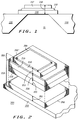
- FIG. 2 is a simplified isometric view of acoustic resonator 201 in accordance with the present invention.
- Acoustic resonator 201 includes quarter-wavelength resonator 203 disposed atop acoustic reflector 218, which, in turn, is disposed atop substrate 255.
- Quarter wavelength resonator 203 comprises electrodes 205, 205' on either side of piezoelectric layer 210. Electrodes 205, 205' and piezoelectric layer 210 have thickness 211 and are atop acoustic reflector 218.
- Acoustic reflector 218 comprises a plurality of layers of material, represented here as layer 215 having thickness 216, layer 220 having thickness 221 and layer 250 having thickness 251. Further layers disposed between layers 220, 250 are denoted by ellipsis. Layer 250 is disposed on substrate 255, analogous to substrate 110 (FIG. 1).
- Layers 215, 220 ... 250 of acoustic reflector 218 are chosen to each have thicknesses 216, 221 ... 251 equal to one-fourth of an acoustic wavelength and are also chosen to have different acoustic impedances, such that in a preferred embodiment acoustic reflector 218 comprises alternating layers of high and low acoustic impedance materials (e.g., layer 250 having higher acoustic impedance than substrate 255).
- Acoustic reflector 218 thus manifests the Ferranti effect, whereby a low impedance (that of substrate 255, for example) at a first end of a transmission line such as acoustic reflector 218 is transformed to a high impedance at a second end (adjacent electrode 205', for example) when acoustic reflector 218 consists of an odd number of layers 215, 220 ... 250.
- a low impedance that of substrate 255, for example
- a transmission line such as acoustic reflector 218
- a second end adjacent electrode 205'
- acoustic reflector 218 may be usefully employed to present a high impedance, analogous to a clamped surface, when acoustic reflector 218 is situated atop a material (e.g., substrate 255) having a low acoustic impedance and when acoustic reflector 218 comprises an odd number of layers each one-fourth of an acoustic wavelength in thickness.
- the effective impedance which acoustic reflector 218 presents increases when the first, third, fifth, etc. layers (e.g., layers 250, 215) have high acoustic impedance and the second, fourth, sixth, etc. layers (e.g., layer 220) have low acoustic impedance.
- acoustic reflector 218 is represented in FIG. 2 as comprising a series of one-fourth wavelength sections
- impedance transformation may be realized through a number of different techniques, such as, by way of example and not intended to be limiting, tapered impedance media (exponentially/hyperbolically/ otherwise tailored impedance profiles may be usefully employed, for example) optimized to provide high impedance or reduced length (thickness) to effect a given impedance transformation, etc. as is known and in accordance with principles discussed, for example, in Chapter 11 and references of Modern Transmission Line Theory and Applications by L. N. Dworsky (John Wiley and Sons: NY, NY, 1979).
- Tapering of acoustic impedance may be effected, for example, by varying the composition of acoustic reflector 218 from an end closest to substrate 255 to an end closest to resonator 203.
- Such variation of composition is usefully realized by sequentially sputtering from a plurality of targets and varying dwell time on each target, or by depositing thin layers of material and varying the number of sequential layers of each material, or by any number of other techniques known in the arts.
- an acoustic resonator disposed at that one end and comprising electrodes 205', 205 and piezoelectric material 210 may usefully be one-fourth of an acoustic wavelength in thickness. This is possible because a lower surface of the acoustic resonator is clamped.
- FIG. 3 is a simplified isometric view of acoustic resonator 301 in accordance with a first preferred embodiment of the present invention.
- Acoustic resonator 301 is analogous to acoustic resonator 203 (FIG. 2) and comprises electrodes 305, 305'' on either side of piezoelectric layer 310 and further comprises electrodes 305'', 305' on either side of piezoelectric layer 310'.
- Piezoelectric layers 310, 310' have thicknesses 320, 320', respectively, wherein thicknesses 320, 320' include thicknesses of electrodes 305, 305', 305''.
- Thicknesses 320, 320' total a thickness of one-fourth of an acoustic wavelength in a first preferred embodiment of the present invention.
- Electrode 305' corresponds to electrode 205' (FIG. 2) and is disposed atop an acoustic reflector such as 218 (FIG.2), for example, in a first preferred embodiment of the present invention.
- Piezoelectric layers 310, 310' (FIG. 3) and 210 (FIG. 2) desirably comprise piezoelectric (or electrostrictive) materials having acceptable electromechanical coupling coefficients, such as, for example, AlN, ZnO, CdS and the like.
- Electrodes 305, 305', 305'' (FIG. 3) and 205, 205' (FIG. 2) are desirably composed of thin layers of metallic materials having low acoustic losses and favorable electrical conductivity properties (e.g., aluminum or aluminum alloys).
- Reflector 218 (FIG. 2) desirably comprises layers of materials having low acoustic propagation losses such as glasses, etc.
- Reflector 218 is conveniently realized as layers of metals because such an arrangement facilitates contacting electrode 205' (FIG. 2) or 305' (FIG. 3), for example, and because metal films are conveniently fabricated and patterned in modern microfabrication facilities. Longitudinal acoustic properties of a few representative materials are summarized in Table I below; comparable shear properties are employed to model resonators using shear vibrational modes.
- stiffness C33 is divided by 1011 and is given in (N/m2), density ⁇ is given in kilograms/m3, longitudinal wave acoustic velocity V a is given in meters/second and acoustic impedance per unit area Z o /A is given in (Watts/m2/(m/s)2) divided by 107.
- Parameters for additional materials are given in a variety of sources such as Air Force Cambridge Research Laboratories Report AFCRL-TR-73-0597, entitled Microwave Acoustics Handbook: Volume 1A. Surface Wave Velocities , by A. Slobodnik et al. and related volumes, which are available from NTIS and/or DTIC, among other places. Further information is also found in Principles of Acoustic Devices , by V. Ristic and in Acoustic Fields and Waves in Solids , Vols. I and II, by B. Auld.
- Electrodes 305, 305', 305'' provide electrical connections to acoustic resonator 301.
- electrodes 305, 305'' may comprise an input electrical port having an associated motional capacitance C m1 while electrodes 305'', 305' may comprise an output electrical port having an associated motional capacitance C m2 .
- FIG. 4 is a graph illustrating relative relative motional capacitances (C m1 , C m2 ) for the first and second portions of resonator structure 301 (FIG. 3) versus the ratio f of thickness of a first resonator element to total resonator thickness in accordance with the first preferred embodiment of the present invention.
- motional capacitance C m1 measured between electrodes 305, 305'' varies as shown by curve 405 of FIG. 4 versus fraction f of thickness 310 compared to (divided by) total thickness 310 + 310', while motional capacitance C m2 measured between electrodes 305', 305'' varies (versus f) as curve 410 where thickness 310' is one-fourth of a wavelength minus thickness 310.
- fraction f is desirably about f ⁇ 0.77, rendering C m1 ⁇ C m2 .
- Fraction f is usefully within about 25% of 0.77, desirably within about 10% of 0.77 and preferably is within about 5% of 0.77, for example.
- FIG. 5 is a graph illustrating relative static shunt capacitance for the first and second portions of the resonator structure of FIG. 3 versus fraction f as defined above (FIG. 4) in accordance with the first preferred embodiment of the present invention.
- curve 505 corresponds to curve 405 while curve 510 corresponds to curve 410.
- Choosing f ⁇ 0.77 provides a capacitance ratio of about 2.5:1.
- a filter incorporating cascaded resonators having a topology input-A1B1-A2B2-output wherein A and B, for example, correspond to the input electrical port and output electrical port, respectively, of the above example, and wherein subscripts 1 and 2 correspond to first and second resonators, respectively, will have asymmetric (i.e., different) input and output electrical impedances.
- a topology such as input-A1B1-B2A2-output may be employed, for example.
- FIG. 6 contains trace 610 describing a measured response taken from an acoustic resonator in accordance with the present invention.
- the axes of FIG. 6 are calibrated in transmitted signal amplitude (ordinate, 0.5 to 0.8) versus frequency in GigaHertz (abscissa, 0.6 to 2.2 GHz).
- Trace 610 shows a sharply defined resonance at a frequency of slightly more than one GigaHertz.
- Measured response 610 is taken from a resonator in accordance with the structure of FIG. 2, wherein three layers of W (corresponding to layers 250, 215) 0.76 micrometers thick are intercalated with two layers of Al (corresponding to layer 220) 0.88 micrometers thick to form an acoustic reflector (corresponding to acoustic reflector 218) on top of a GaAs substrate (corresponding to substrate 255).
- W and Al were chosen for these layers because they provide a substantial acoustic impedance ratio (see Table I, supra), they facilitate electrical contact and they are convenient for fabrication.
- a layer of ZnO (corresponding to piezoelectric layer 210) 0.84 micrometer thick was disposed atop the acoustic reflector.
- Thin layers (ca. 1000 Angstroms) of silicon nitride were deposited by plasma-enhanced chemical vapor deposition above the top W layer and atop the ZnO layer in order to protect them from etchants used to pattern various portions of the experimental resonator structure.
- the ZnO layer is etched with HNO3:HCl:H2O (3:1:4 by volume) which may attack W, Al and/or GaAs, which are protected from such attack by the underlying silicon nitride layer.
- the W and Al layers are patterned using etchants well known in the microfabrication arts.
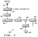
- FIG. 7 is a simplified schematic diagram indicating how the above-described acoustic filters according to the present invention are advantageously used in radio frequency circuit 890.
- Radio frequency circuit 890 comprises antenna 891 sending or receiving signals from optional diplexer 892 (which is coupled to the transmitter if one is used).
- Diplexer 892 sends an incoming signal to filter 893 which passes the resulting band limited signal to amplifier 894. From amplifier 894 the signal passes through another band limiting filter 895 to mixer 896.
- Mixer 896 also receives a signal from local oscillator 897 through band limiting filter 898. The mixed signal from mixer 896 passes through band limiting filter 899 which removes the local oscillator signal and sends the result to the receiver IF via output 800.
- Filters 893, 895, 898 and/or 899 are advantageously thin film resonator filters of the type described here and made according to the structure and method of the present invention, but of varying frequency or other properties according to the particular desired function.
- filter 893 removes input RF frequencies outside the band in which the receiver is intended to operate. This is particularly useful for narrow band receivers such as are frequently required in cellular phone and paging applications and the like.
- local oscillator 897 may employ a thin film resonator in accordance with the present invention for a frequency stabilizing element.
- Filter 895 may have the same or a different pass band than filter 893 and removes any undesired harmonics generated by amplifier 894 or other out-of-band signals not removed by filter 893.
- Filter 898 desirably passes the LO frequency and stops undesired harmonics thereof.
- Filter 899 desirably passes the sum or difference frequencies produced by mixer 896, and blocks the local oscillator and input RF frequencies. This is important to avoid saturating the input stages of the IF amplifier which is typically coupled to output 800.
- electronic apparatus, and especially radios have improved properties as a result of the improved properties of the thin film resonator filters of the present invention.
Landscapes
- Physics & Mathematics (AREA)
- Acoustics & Sound (AREA)
- Piezo-Electric Or Mechanical Vibrators, Or Delay Or Filter Circuits (AREA)
- Obtaining Desirable Characteristics In Audible-Bandwidth Transducers (AREA)
Applications Claiming Priority (2)
| Application Number | Priority Date | Filing Date | Title |
|---|---|---|---|
| US11924 | 1993-02-01 | ||
| US08/011,924 US5373268A (en) | 1993-02-01 | 1993-02-01 | Thin film resonator having stacked acoustic reflecting impedance matching layers and method |
Publications (3)
| Publication Number | Publication Date |
|---|---|
| EP0609555A2 true EP0609555A2 (de) | 1994-08-10 |
| EP0609555A3 EP0609555A3 (de) | 1995-08-23 |
| EP0609555B1 EP0609555B1 (de) | 1999-10-27 |
Family
ID=21752549
Family Applications (1)
| Application Number | Title | Priority Date | Filing Date |
|---|---|---|---|
| EP93120778A Expired - Lifetime EP0609555B1 (de) | 1993-02-01 | 1993-12-23 | Frequenzselektives Verfahren und Vorrichtung |
Country Status (4)
| Country | Link |
|---|---|
| US (1) | US5373268A (de) |
| EP (1) | EP0609555B1 (de) |
| JP (1) | JP3119287B2 (de) |
| DE (1) | DE69326880T2 (de) |
Cited By (17)
| Publication number | Priority date | Publication date | Assignee | Title |
|---|---|---|---|---|
| EP0834989A3 (de) * | 1996-10-02 | 1998-05-06 | Nokia Mobile Phones Ltd. | Anordnung mit abstimmbarem Dünnfilmresonator mit akustischen Volumenwellen für Amplituden- und Phasenmodulation |
| EP0865157A2 (de) | 1997-03-13 | 1998-09-16 | Nokia Mobile Phones Ltd. | Akustisches Volumenwellenfilter |
| US5873154A (en) * | 1996-10-17 | 1999-02-23 | Nokia Mobile Phones Limited | Method for fabricating a resonator having an acoustic mirror |
| US5910756A (en) * | 1997-05-21 | 1999-06-08 | Nokia Mobile Phones Limited | Filters and duplexers utilizing thin film stacked crystal filter structures and thin film bulk acoustic wave resonators |
| US6051907A (en) * | 1996-10-10 | 2000-04-18 | Nokia Mobile Phones Limited | Method for performing on-wafer tuning of thin film bulk acoustic wave resonators (FBARS) |
| US6081171A (en) * | 1998-04-08 | 2000-06-27 | Nokia Mobile Phones Limited | Monolithic filters utilizing thin film bulk acoustic wave devices and minimum passive components for controlling the shape and width of a passband response |
| EP1067685A3 (de) * | 1999-07-07 | 2001-06-27 | Philips Corporate Intellectual Property GmbH | Volumenwellen-Filter |
| WO2001063759A1 (en) * | 2000-02-22 | 2001-08-30 | Koninklijke Philips Electronics N.V. | Method of manufacturing a piezoeletric filter with an acoustic resonator situated on an acoustic reflector layer formed on a carrier substrate |
| EP1126602A3 (de) * | 2000-02-18 | 2002-01-09 | Infineon Technologies AG | Piezoresonator |
| WO2003017480A1 (de) * | 2001-08-14 | 2003-02-27 | Koninklijke Philips Electronics N.V. | Filteranordnung mit volumenwellen-resonator |
| WO2003032486A1 (de) * | 2001-10-08 | 2003-04-17 | Infineon Technologies Ag | Baw-resonator |
| EP1419577A1 (de) * | 2001-08-14 | 2004-05-19 | Koninklijke Philips Electronics N.V. | Filteranordnung mit volumenwellen-resonator |
| US6839946B2 (en) | 1996-10-17 | 2005-01-11 | Nokia Corporation | Method for fabricating a thin film bulk acoustic wave resonator (FBAR) on a glass substrate |
| US6933807B2 (en) | 2002-11-07 | 2005-08-23 | Infineon Technologies Ag | Acoustic reflector for a BAW resonator providing specified reflection of both shear waves and longitudinal waves |
| US7304551B2 (en) | 2002-11-08 | 2007-12-04 | Murata Manufacturing Co., Ltd. | Branching filter and communication device |
| WO2009073049A1 (en) * | 2007-12-04 | 2009-06-11 | Maxim Integrated Products, Inc. | Optimal acoustic impedance materials for polished substrate coating to suppress passband ripple in baw resonators and filters |
| US7768364B2 (en) | 2008-06-09 | 2010-08-03 | Maxim Integrated Products, Inc. | Bulk acoustic resonators with multi-layer electrodes |
Families Citing this family (63)
| Publication number | Priority date | Publication date | Assignee | Title |
|---|---|---|---|---|
| JP3344441B2 (ja) * | 1994-03-25 | 2002-11-11 | 住友電気工業株式会社 | 表面弾性波素子 |
| US5864261A (en) * | 1994-05-23 | 1999-01-26 | Iowa State University Research Foundation | Multiple layer acoustical structures for thin-film resonator based circuits and systems |
| US5596239A (en) * | 1995-06-29 | 1997-01-21 | Motorola, Inc. | Enhanced quality factor resonator |
| US5617065A (en) * | 1995-06-29 | 1997-04-01 | Motorola, Inc. | Filter using enhanced quality factor resonator and method |
| US5696423A (en) * | 1995-06-29 | 1997-12-09 | Motorola, Inc. | Temperature compenated resonator and method |
| US5821833A (en) * | 1995-12-26 | 1998-10-13 | Tfr Technologies, Inc. | Stacked crystal filter device and method of making |
| US5646583A (en) * | 1996-01-04 | 1997-07-08 | Rockwell International Corporation | Acoustic isolator having a high impedance layer of hafnium oxide |
| US5760663A (en) * | 1996-08-23 | 1998-06-02 | Motorola, Inc. | Elliptic baw resonator filter and method of making the same |
| US6087198A (en) * | 1998-02-12 | 2000-07-11 | Texas Instruments Incorporated | Low cost packaging for thin-film resonators and thin-film resonator-based filters |
| FI106894B (fi) | 1998-06-02 | 2001-04-30 | Nokia Mobile Phones Ltd | Resonaattorirakenteita |
| FI108583B (fi) | 1998-06-02 | 2002-02-15 | Nokia Corp | Resonaattorirakenteita |
| FI113211B (fi) * | 1998-12-30 | 2004-03-15 | Nokia Corp | Balansoitu suodatinrakenne ja matkaviestinlaite |
| FI107660B (fi) | 1999-07-19 | 2001-09-14 | Nokia Mobile Phones Ltd | Resonaattorirakenne |
| US6107721A (en) * | 1999-07-27 | 2000-08-22 | Tfr Technologies, Inc. | Piezoelectric resonators on a differentially offset reflector |
| DE19947081A1 (de) * | 1999-09-30 | 2001-04-05 | Infineon Technologies Ag | Akustischer Spiegel und Verfahren zu dessen Herstellung |
| US6307447B1 (en) | 1999-11-01 | 2001-10-23 | Agere Systems Guardian Corp. | Tuning mechanical resonators for electrical filter |
| US6339276B1 (en) * | 1999-11-01 | 2002-01-15 | Agere Systems Guardian Corp. | Incremental tuning process for electrical resonators based on mechanical motion |
| FI107661B (fi) | 1999-11-29 | 2001-09-14 | Nokia Mobile Phones Ltd | Menetelmä balansoidun suotimen keskitaajuuden säätämiseksi ja joukko balansoituja suotimia |
| US6746577B1 (en) | 1999-12-16 | 2004-06-08 | Agere Systems, Inc. | Method and apparatus for thickness control and reproducibility of dielectric film deposition |
| US6524971B1 (en) | 1999-12-17 | 2003-02-25 | Agere Systems, Inc. | Method of deposition of films |
| US6441703B1 (en) | 2000-01-18 | 2002-08-27 | Texas Instruments Incorporated | Multiple frequency acoustic reflector array and monolithic cover for resonators and method |
| US6452310B1 (en) | 2000-01-18 | 2002-09-17 | Texas Instruments Incorporated | Thin film resonator and method |
| US6306313B1 (en) | 2000-02-04 | 2001-10-23 | Agere Systems Guardian Corp. | Selective etching of thin films |
| US6323744B1 (en) | 2000-02-04 | 2001-11-27 | Agere Systems Guardian Corp. | Grounding of TFR ladder filters |
| US6377136B1 (en) | 2000-02-04 | 2002-04-23 | Agere Systems Guardian Corporation | Thin film resonator filter having at least one component with different resonant frequency sets or electrode capacitance |
| US7296329B1 (en) | 2000-02-04 | 2007-11-20 | Agere Systems Inc. | Method of isolation for acoustic resonator device |
| US6437667B1 (en) | 2000-02-04 | 2002-08-20 | Agere Systems Guardian Corp. | Method of tuning thin film resonator filters by removing or adding piezoelectric material |
| US6329305B1 (en) * | 2000-02-11 | 2001-12-11 | Agere Systems Guardian Corp. | Method for producing devices having piezoelectric films |
| US6603241B1 (en) * | 2000-05-23 | 2003-08-05 | Agere Systems, Inc. | Acoustic mirror materials for acoustic devices |
| US6355498B1 (en) | 2000-08-11 | 2002-03-12 | Agere Systems Guartian Corp. | Thin film resonators fabricated on membranes created by front side releasing |
| US6486751B1 (en) | 2000-09-26 | 2002-11-26 | Agere Systems Inc. | Increased bandwidth thin film resonator having a columnar structure |
| US6674291B1 (en) | 2000-10-30 | 2004-01-06 | Agere Systems Guardian Corp. | Method and apparatus for determining and/or improving high power reliability in thin film resonator devices, and a thin film resonator device resultant therefrom |
| US6587212B1 (en) | 2000-10-31 | 2003-07-01 | Agere Systems Inc. | Method and apparatus for studying vibrational modes of an electro-acoustic device |
| US6743731B1 (en) * | 2000-11-17 | 2004-06-01 | Agere Systems Inc. | Method for making a radio frequency component and component produced thereby |
| FI113111B (fi) | 2000-11-24 | 2004-02-27 | Nokia Corp | Pietsosähköisiä resonaattoreita käsittävä suodinrakenne ja järjestely |
| US6509813B2 (en) * | 2001-01-16 | 2003-01-21 | Nokia Mobile Phones Ltd. | Bulk acoustic wave resonator with a conductive mirror |
| US7435613B2 (en) | 2001-02-12 | 2008-10-14 | Agere Systems Inc. | Methods of fabricating a membrane with improved mechanical integrity |
| US6469597B2 (en) * | 2001-03-05 | 2002-10-22 | Agilent Technologies, Inc. | Method of mass loading of thin film bulk acoustic resonators (FBAR) for creating resonators of different frequencies and apparatus embodying the method |
| US6601276B2 (en) | 2001-05-11 | 2003-08-05 | Agere Systems Inc. | Method for self alignment of patterned layers in thin film acoustic devices |
| JP2005236337A (ja) | 2001-05-11 | 2005-09-02 | Ube Ind Ltd | 薄膜音響共振器及びその製造方法 |
| US6720844B1 (en) | 2001-11-16 | 2004-04-13 | Tfr Technologies, Inc. | Coupled resonator bulk acoustic wave filter |
| JP2004222244A (ja) | 2002-12-27 | 2004-08-05 | Toshiba Corp | 薄膜圧電共振器およびその製造方法 |
| JP4024741B2 (ja) | 2003-10-20 | 2007-12-19 | 富士通メディアデバイス株式会社 | 圧電薄膜共振子及びフィルタ |
| US7235915B2 (en) * | 2003-11-18 | 2007-06-26 | Matsushita Electric Industrial Co., Ltd. | Acoustic resonator device, filter device, manufacturing method for acoustic resonator device, and communication apparatus |
| JP2005244184A (ja) * | 2004-01-28 | 2005-09-08 | Toshiba Corp | 薄膜圧電素子及び薄膜圧電素子の製造方法 |
| US7323805B2 (en) | 2004-01-28 | 2008-01-29 | Kabushiki Kaisha Toshiba | Piezoelectric thin film device and method for manufacturing the same |
| US7227433B2 (en) * | 2004-03-31 | 2007-06-05 | Intel Corporation | Electro mechanical device having a sealed cavity |
| US7554422B2 (en) * | 2004-09-10 | 2009-06-30 | Panasonic Corporation | Filter module using piezoelectric resonators, duplexer, communication device, and method for fabricating filter module |
| JP4548088B2 (ja) * | 2004-10-20 | 2010-09-22 | セイコーエプソン株式会社 | 弾性表面波装置 |
| US20060220763A1 (en) * | 2005-03-31 | 2006-10-05 | Tomohiro Iwasaki | Acoustic mirror type thin film bulk acoustic resonator, and filter, duplexer and communication apparatus comprising the same |
| JPWO2007004435A1 (ja) * | 2005-06-30 | 2009-01-22 | パナソニック株式会社 | 音響共振器及びフィルタ |
| US20070035364A1 (en) * | 2005-08-11 | 2007-02-15 | Uppili Sridhar | Titanium-tungsten alloy based mirrors and electrodes in bulk acoustic wave devices |
| DE102006023165B4 (de) | 2006-05-17 | 2008-02-14 | Infineon Technologies Ag | Verfahren zur Herstellung eines akustischen Spiegels aus alternierend angeordneten Schichten hoher und niedriger akustischer Impedanz |
| US20090053401A1 (en) * | 2007-08-24 | 2009-02-26 | Maxim Integrated Products, Inc. | Piezoelectric deposition for BAW resonators |
| US7567024B2 (en) * | 2007-09-26 | 2009-07-28 | Maxim Integrated Products, Inc. | Methods of contacting the top layer of a BAW resonator |
| JP2013201346A (ja) * | 2012-03-26 | 2013-10-03 | Ulvac Japan Ltd | 圧電素子及び圧電素子の製造方法 |
| US10658998B2 (en) | 2013-07-31 | 2020-05-19 | Oepic Semiconductors, Inc. | Piezoelectric film transfer for acoustic resonators and filters |
| US10178459B2 (en) | 2016-03-09 | 2019-01-08 | Mrspeakers, Llc | Loudspeaker with acoustic impedance system |
| US11394361B2 (en) | 2019-02-25 | 2022-07-19 | Texas Instruments Incorporated | Buk acoustic wave resonator with guard rings having recessed space from electrode edge and periodic designs |
| US11264970B2 (en) | 2019-03-02 | 2022-03-01 | Texas Instruments Incorporated | Piezoelectric resonator with patterned resonant confiners |
| US11190164B2 (en) | 2019-05-24 | 2021-11-30 | Texas Instruments Incorporated | Using acoustic reflector to reduce spurious modes |
| US11356082B2 (en) | 2019-12-12 | 2022-06-07 | Texas Instruments Incorporated | Folded ramp generator |
| US12483222B2 (en) | 2023-02-24 | 2025-11-25 | Texas Instruments Incorporated | Spurious mode reduction for electromechanical resonator circuit |
Family Cites Families (17)
| Publication number | Priority date | Publication date | Assignee | Title |
|---|---|---|---|---|
| US3414832A (en) * | 1964-12-04 | 1968-12-03 | Westinghouse Electric Corp | Acoustically resonant device |
| US3313959A (en) * | 1966-08-08 | 1967-04-11 | Hughes Aircraft Co | Thin-film resonance device |
| US3422371A (en) * | 1967-07-24 | 1969-01-14 | Sanders Associates Inc | Thin film piezoelectric oscillator |
| AT353506B (de) * | 1976-10-19 | 1979-11-26 | List Hans | Piezoelektrischer resonator |
| US4460756A (en) * | 1981-04-02 | 1984-07-17 | Phillips Petroleum Company | Olefin polymerization method |
| JPS58137319A (ja) * | 1982-02-09 | 1983-08-15 | Nec Corp | 高周波圧電振動子 |
| JPS58137317A (ja) * | 1982-02-09 | 1983-08-15 | Nec Corp | 圧電薄膜複合振動子 |
| US4556812A (en) * | 1983-10-13 | 1985-12-03 | The United States Of America As Represented By The United States Department Of Energy | Acoustic resonator with Al electrodes on an AlN layer and using a GaAs substrate |
| US4502932A (en) * | 1983-10-13 | 1985-03-05 | The United States Of America As Represented By The United States Department Of Energy | Acoustic resonator and method of making same |
| JPS60100950A (ja) * | 1983-11-09 | 1985-06-04 | 松下電器産業株式会社 | 超音波探触子 |
| JPS60189307A (ja) * | 1984-03-09 | 1985-09-26 | Toshiba Corp | 圧電薄膜共振器およびその製造方法 |
| DE3501808A1 (de) * | 1985-01-21 | 1986-07-24 | Siemens AG, 1000 Berlin und 8000 München | Ultraschallwandler |
| US4719383A (en) * | 1985-05-20 | 1988-01-12 | The United States Of America As Represented By The United States Department Of Energy | Piezoelectric shear wave resonator and method of making same |
| US4749900A (en) * | 1986-11-17 | 1988-06-07 | The Board Of Trustees Of The Leland Stanford Junior University | Multi-layer acoustic transducer for high frequency ultrasound |
| US5011568A (en) * | 1990-06-11 | 1991-04-30 | Iowa State University Research Foundation, Inc. | Use of sol-gel derived tantalum oxide as a protective coating for etching silicon |
| US5075641A (en) * | 1990-12-04 | 1991-12-24 | Iowa State University Research Foundation, Inc. | High frequency oscillator comprising cointegrated thin film resonator and active device |
| US5162691A (en) * | 1991-01-22 | 1992-11-10 | The United States Of America As Represented By The Secretary Of The Army | Cantilevered air-gap type thin film piezoelectric resonator |
-
1993
- 1993-02-01 US US08/011,924 patent/US5373268A/en not_active Expired - Fee Related
- 1993-12-23 EP EP93120778A patent/EP0609555B1/de not_active Expired - Lifetime
- 1993-12-23 DE DE69326880T patent/DE69326880T2/de not_active Expired - Fee Related
-
1994
- 1994-01-28 JP JP06024973A patent/JP3119287B2/ja not_active Expired - Fee Related
Cited By (25)
| Publication number | Priority date | Publication date | Assignee | Title |
|---|---|---|---|---|
| EP0834989A3 (de) * | 1996-10-02 | 1998-05-06 | Nokia Mobile Phones Ltd. | Anordnung mit abstimmbarem Dünnfilmresonator mit akustischen Volumenwellen für Amplituden- und Phasenmodulation |
| US6051907A (en) * | 1996-10-10 | 2000-04-18 | Nokia Mobile Phones Limited | Method for performing on-wafer tuning of thin film bulk acoustic wave resonators (FBARS) |
| US5873154A (en) * | 1996-10-17 | 1999-02-23 | Nokia Mobile Phones Limited | Method for fabricating a resonator having an acoustic mirror |
| US6839946B2 (en) | 1996-10-17 | 2005-01-11 | Nokia Corporation | Method for fabricating a thin film bulk acoustic wave resonator (FBAR) on a glass substrate |
| EP0865157A3 (de) * | 1997-03-13 | 2000-04-05 | Nokia Mobile Phones Ltd. | Akustisches Volumenwellenfilter |
| US5872493A (en) * | 1997-03-13 | 1999-02-16 | Nokia Mobile Phones, Ltd. | Bulk acoustic wave (BAW) filter having a top portion that includes a protective acoustic mirror |
| EP0865157A2 (de) | 1997-03-13 | 1998-09-16 | Nokia Mobile Phones Ltd. | Akustisches Volumenwellenfilter |
| US5910756A (en) * | 1997-05-21 | 1999-06-08 | Nokia Mobile Phones Limited | Filters and duplexers utilizing thin film stacked crystal filter structures and thin film bulk acoustic wave resonators |
| US6081171A (en) * | 1998-04-08 | 2000-06-27 | Nokia Mobile Phones Limited | Monolithic filters utilizing thin film bulk acoustic wave devices and minimum passive components for controlling the shape and width of a passband response |
| EP1067685A3 (de) * | 1999-07-07 | 2001-06-27 | Philips Corporate Intellectual Property GmbH | Volumenwellen-Filter |
| US6466105B1 (en) | 1999-07-07 | 2002-10-15 | Koninklijke Philips Electronics N.V. | Bulk acoustic wave filter |
| EP1126602A3 (de) * | 2000-02-18 | 2002-01-09 | Infineon Technologies AG | Piezoresonator |
| US6534900B2 (en) | 2000-02-18 | 2003-03-18 | Infineon Technologies Ag | Piezoresonator |
| WO2001063759A1 (en) * | 2000-02-22 | 2001-08-30 | Koninklijke Philips Electronics N.V. | Method of manufacturing a piezoeletric filter with an acoustic resonator situated on an acoustic reflector layer formed on a carrier substrate |
| WO2003017480A1 (de) * | 2001-08-14 | 2003-02-27 | Koninklijke Philips Electronics N.V. | Filteranordnung mit volumenwellen-resonator |
| EP1419577A1 (de) * | 2001-08-14 | 2004-05-19 | Koninklijke Philips Electronics N.V. | Filteranordnung mit volumenwellen-resonator |
| CN100361386C (zh) * | 2001-08-14 | 2008-01-09 | Nxp股份有限公司 | 带有体波谐振器的滤波系统及其相关装置 |
| WO2003032486A1 (de) * | 2001-10-08 | 2003-04-17 | Infineon Technologies Ag | Baw-resonator |
| US6975183B2 (en) | 2001-10-08 | 2005-12-13 | Infineon Technologies Ag | BAW resonator having piezoelectric layers oriented in opposed directions |
| US6933807B2 (en) | 2002-11-07 | 2005-08-23 | Infineon Technologies Ag | Acoustic reflector for a BAW resonator providing specified reflection of both shear waves and longitudinal waves |
| US7304551B2 (en) | 2002-11-08 | 2007-12-04 | Murata Manufacturing Co., Ltd. | Branching filter and communication device |
| WO2009073049A1 (en) * | 2007-12-04 | 2009-06-11 | Maxim Integrated Products, Inc. | Optimal acoustic impedance materials for polished substrate coating to suppress passband ripple in baw resonators and filters |
| US8512800B2 (en) | 2007-12-04 | 2013-08-20 | Triquint Semiconductor, Inc. | Optimal acoustic impedance materials for polished substrate coating to suppress passband ripple in BAW resonators and filters |
| US8952768B2 (en) | 2007-12-04 | 2015-02-10 | Triquint Semiconductor, Inc. | Optimal acoustic impedance materials for polished substrate coating to suppress passband ripple in BAW resonators and filters |
| US7768364B2 (en) | 2008-06-09 | 2010-08-03 | Maxim Integrated Products, Inc. | Bulk acoustic resonators with multi-layer electrodes |
Also Published As
| Publication number | Publication date |
|---|---|
| DE69326880D1 (de) | 1999-12-02 |
| JPH06295181A (ja) | 1994-10-21 |
| US5373268A (en) | 1994-12-13 |
| DE69326880T2 (de) | 2000-04-20 |
| EP0609555A3 (de) | 1995-08-23 |
| JP3119287B2 (ja) | 2000-12-18 |
| EP0609555B1 (de) | 1999-10-27 |
Similar Documents
| Publication | Publication Date | Title |
|---|---|---|
| EP0609555B1 (de) | Frequenzselektives Verfahren und Vorrichtung | |
| US6548942B1 (en) | Encapsulated packaging for thin-film resonators and thin-film resonator-based filters having a piezoelectric resonator between two acoustic reflectors | |
| Lakin et al. | Development of miniature filters for wireless applications | |
| Reeder et al. | Characteristics of microwave acoustic transducers for volume wave excitation | |
| Weigel et al. | Microwave acoustic materials, devices, and applications | |
| US9391588B2 (en) | MEMS vibrating structure using an orientation dependent single-crystal piezoelectric thin film layer | |
| EP0973256B1 (de) | Piezoelektrische dünnschichtanordnung | |
| US8829766B2 (en) | Piezoelectric resonator operating in thickness shear mode | |
| Krishnaswamy et al. | Film bulk acoustic wave resonator technology | |
| US5884378A (en) | Method of making an enhanced quality factor resonator | |
| US7463117B2 (en) | Film bulk acoustic-wave resonator (FBAR), filter implemented by FBARs and method for manufacturing FBAR | |
| US5617065A (en) | Filter using enhanced quality factor resonator and method | |
| KR20040051539A (ko) | 압전 공진 필터 및 듀플렉서 | |
| US10658998B2 (en) | Piezoelectric film transfer for acoustic resonators and filters | |
| US9385685B2 (en) | MEMS vibrating structure using an orientation dependent single-crystal piezoelectric thin film layer | |
| Gokhale et al. | GaN-based periodic high-Q RF acoustic resonator with integrated HEMT | |
| JP2001044794A (ja) | 圧電共振子 | |
| Barrera et al. | Frequency and bandwidth design toward millimeter-wave thin-film lithium niobate acoustic filters | |
| Lakin | Thin film resonators and high frequency filters | |
| JP2002374145A (ja) | 圧電薄膜共振子 | |
| KR0158898B1 (ko) | 전자음향집적회로와 그 제조방법 | |
| US20250088166A1 (en) | Bulk acoustic wave resonator, manufacturing method thereof and electronic device | |
| KR100446845B1 (ko) | 박막 압전 소자 | |
| JP2001285021A (ja) | 弾性表面波装置 | |
| Lakin et al. | Thin film bulk acoustic wave resonator and filter technology |
Legal Events
| Date | Code | Title | Description |
|---|---|---|---|
| PUAI | Public reference made under article 153(3) epc to a published international application that has entered the european phase |
Free format text: ORIGINAL CODE: 0009012 |
|
| AK | Designated contracting states |
Kind code of ref document: A2 Designated state(s): DE FR GB |
|
| PUAL | Search report despatched |
Free format text: ORIGINAL CODE: 0009013 |
|
| AK | Designated contracting states |
Kind code of ref document: A3 Designated state(s): DE FR GB |
|
| 17P | Request for examination filed |
Effective date: 19960409 |
|
| 17Q | First examination report despatched |
Effective date: 19980326 |
|
| GRAG | Despatch of communication of intention to grant |
Free format text: ORIGINAL CODE: EPIDOS AGRA |
|
| GRAG | Despatch of communication of intention to grant |
Free format text: ORIGINAL CODE: EPIDOS AGRA |
|
| GRAH | Despatch of communication of intention to grant a patent |
Free format text: ORIGINAL CODE: EPIDOS IGRA |
|
| GRAH | Despatch of communication of intention to grant a patent |
Free format text: ORIGINAL CODE: EPIDOS IGRA |
|
| GRAA | (expected) grant |
Free format text: ORIGINAL CODE: 0009210 |
|
| AK | Designated contracting states |
Kind code of ref document: B1 Designated state(s): DE FR GB |
|
| REF | Corresponds to: |
Ref document number: 69326880 Country of ref document: DE Date of ref document: 19991202 |
|
| ET | Fr: translation filed | ||
| PLBE | No opposition filed within time limit |
Free format text: ORIGINAL CODE: 0009261 |
|
| STAA | Information on the status of an ep patent application or granted ep patent |
Free format text: STATUS: NO OPPOSITION FILED WITHIN TIME LIMIT |
|
| 26N | No opposition filed | ||
| REG | Reference to a national code |
Ref country code: GB Ref legal event code: IF02 |
|
| PGFP | Annual fee paid to national office [announced via postgrant information from national office to epo] |
Ref country code: GB Payment date: 20021104 Year of fee payment: 10 |
|
| PGFP | Annual fee paid to national office [announced via postgrant information from national office to epo] |
Ref country code: FR Payment date: 20021202 Year of fee payment: 10 |
|
| PGFP | Annual fee paid to national office [announced via postgrant information from national office to epo] |
Ref country code: DE Payment date: 20021230 Year of fee payment: 10 |
|
| PG25 | Lapsed in a contracting state [announced via postgrant information from national office to epo] |
Ref country code: GB Free format text: LAPSE BECAUSE OF NON-PAYMENT OF DUE FEES Effective date: 20031223 |
|
| PG25 | Lapsed in a contracting state [announced via postgrant information from national office to epo] |
Ref country code: DE Free format text: LAPSE BECAUSE OF NON-PAYMENT OF DUE FEES Effective date: 20040701 |
|
| GBPC | Gb: european patent ceased through non-payment of renewal fee |
Effective date: 20031223 |
|
| PG25 | Lapsed in a contracting state [announced via postgrant information from national office to epo] |
Ref country code: FR Free format text: LAPSE BECAUSE OF NON-PAYMENT OF DUE FEES Effective date: 20040831 |
|
| REG | Reference to a national code |
Ref country code: FR Ref legal event code: ST |