EP0865157A2 - Akustisches Volumenwellenfilter - Google Patents
Akustisches Volumenwellenfilter Download PDFInfo
- Publication number
- EP0865157A2 EP0865157A2 EP98301934A EP98301934A EP0865157A2 EP 0865157 A2 EP0865157 A2 EP 0865157A2 EP 98301934 A EP98301934 A EP 98301934A EP 98301934 A EP98301934 A EP 98301934A EP 0865157 A2 EP0865157 A2 EP 0865157A2
- Authority
- EP
- European Patent Office
- Prior art keywords
- resonator
- baw
- acoustic
- baw filter
- set forth
- Prior art date
- Legal status (The legal status is an assumption and is not a legal conclusion. Google has not performed a legal analysis and makes no representation as to the accuracy of the status listed.)
- Granted
Links
Images


Classifications
-
- H—ELECTRICITY
- H03—ELECTRONIC CIRCUITRY
- H03H—IMPEDANCE NETWORKS, e.g. RESONANT CIRCUITS; RESONATORS
- H03H9/00—Networks comprising electromechanical or electro-acoustic elements; Electromechanical resonators
- H03H9/46—Filters
- H03H9/54—Filters comprising resonators of piezoelectric or electrostrictive material
- H03H9/58—Multiple crystal filters
- H03H9/582—Multiple crystal filters implemented with thin-film techniques
- H03H9/586—Means for mounting to a substrate, i.e. means constituting the material interface confining the waves to a volume
- H03H9/589—Acoustic mirrors
-
- H—ELECTRICITY
- H03—ELECTRONIC CIRCUITRY
- H03H—IMPEDANCE NETWORKS, e.g. RESONANT CIRCUITS; RESONATORS
- H03H3/00—Apparatus or processes specially adapted for the manufacture of impedance networks, resonating circuits, resonators
- H03H3/007—Apparatus or processes specially adapted for the manufacture of impedance networks, resonating circuits, resonators for the manufacture of electromechanical resonators or networks
- H03H3/02—Apparatus or processes specially adapted for the manufacture of impedance networks, resonating circuits, resonators for the manufacture of electromechanical resonators or networks for the manufacture of piezoelectric or electrostrictive resonators or networks
-
- H—ELECTRICITY
- H03—ELECTRONIC CIRCUITRY
- H03H—IMPEDANCE NETWORKS, e.g. RESONANT CIRCUITS; RESONATORS
- H03H9/00—Networks comprising electromechanical or electro-acoustic elements; Electromechanical resonators
- H03H9/02—Details
- H03H9/05—Holders or supports
- H03H9/0504—Holders or supports for bulk acoustic wave devices
- H03H9/0514—Holders or supports for bulk acoustic wave devices consisting of mounting pads or bumps
- H03H9/0523—Holders or supports for bulk acoustic wave devices consisting of mounting pads or bumps for flip-chip mounting
-
- H—ELECTRICITY
- H03—ELECTRONIC CIRCUITRY
- H03H—IMPEDANCE NETWORKS, e.g. RESONANT CIRCUITS; RESONATORS
- H03H9/00—Networks comprising electromechanical or electro-acoustic elements; Electromechanical resonators
- H03H9/02—Details
- H03H9/05—Holders or supports
- H03H9/0504—Holders or supports for bulk acoustic wave devices
- H03H9/0528—Holders or supports for bulk acoustic wave devices consisting of clips
-
- H—ELECTRICITY
- H03—ELECTRONIC CIRCUITRY
- H03H—IMPEDANCE NETWORKS, e.g. RESONANT CIRCUITS; RESONATORS
- H03H9/00—Networks comprising electromechanical or electro-acoustic elements; Electromechanical resonators
- H03H9/46—Filters
- H03H9/54—Filters comprising resonators of piezoelectric or electrostrictive material
- H03H9/58—Multiple crystal filters
- H03H9/582—Multiple crystal filters implemented with thin-film techniques
- H03H9/583—Multiple crystal filters implemented with thin-film techniques comprising a plurality of piezoelectric layers acoustically coupled
- H03H9/585—Stacked Crystal Filters [SCF]
-
- H—ELECTRICITY
- H03—ELECTRONIC CIRCUITRY
- H03H—IMPEDANCE NETWORKS, e.g. RESONANT CIRCUITS; RESONATORS
- H03H9/00—Networks comprising electromechanical or electro-acoustic elements; Electromechanical resonators
- H03H9/46—Filters
- H03H9/54—Filters comprising resonators of piezoelectric or electrostrictive material
- H03H9/58—Multiple crystal filters
- H03H9/60—Electric coupling means therefor
- H03H9/605—Electric coupling means therefor consisting of a ladder configuration
-
- H—ELECTRICITY
- H10—SEMICONDUCTOR DEVICES; ELECTRIC SOLID-STATE DEVICES NOT OTHERWISE PROVIDED FOR
- H10W—GENERIC PACKAGES, INTERCONNECTIONS, CONNECTORS OR OTHER CONSTRUCTIONAL DETAILS OF DEVICES COVERED BY CLASS H10
- H10W90/00—Package configurations
- H10W90/701—Package configurations characterised by the relative positions of pads or connectors relative to package parts
- H10W90/721—Package configurations characterised by the relative positions of pads or connectors relative to package parts of bump connectors
- H10W90/724—Package configurations characterised by the relative positions of pads or connectors relative to package parts of bump connectors between a chip and a stacked insulating package substrate, interposer or RDL
-
- H—ELECTRICITY
- H10—SEMICONDUCTOR DEVICES; ELECTRIC SOLID-STATE DEVICES NOT OTHERWISE PROVIDED FOR
- H10W—GENERIC PACKAGES, INTERCONNECTIONS, CONNECTORS OR OTHER CONSTRUCTIONAL DETAILS OF DEVICES COVERED BY CLASS H10
- H10W90/00—Package configurations
- H10W90/701—Package configurations characterised by the relative positions of pads or connectors relative to package parts
- H10W90/751—Package configurations characterised by the relative positions of pads or connectors relative to package parts of bond wires
- H10W90/754—Package configurations characterised by the relative positions of pads or connectors relative to package parts of bond wires between a chip and a stacked insulating package substrate, interposer or RDL
Definitions
- the present invention relates to Bulk Acoustic Wave (BAW) filters.
- BAW Bulk Acoustic Wave
- SMT Surface Mount Technology
- SAW Surface Acoustic Wave
- Another known method of protecting layer surfaces of SAW filters includes packaging the SAW filters in hermetically sealed ceramic packages. After being packaged in this manner, the SAW filters can then be surface mounted to a circuit board. Unfortunately, this technique tends to be expensive, as packaging costs can contribute considerably to overall fabrication costs.
- BAW filters typically include several BAW resonators.
- acoustic waves propagate in a direction that is perpendicular to the filter's layer surfaces.
- acoustic waves which propagate within a SAW filter do so in a direction that is parallel to the layer surfaces of the filter.
- the performance of a SAW filter is likely to be more detrimentally effected when its layer surfaces are contaminated or otherwise impaired by external elements than would be the performance of a BAW filter that experiences similar contamination.
- BAW filters can be fabricated to include various known types of BAW resonators. These known types of BAW resonators comprise three basic portions.
- a second one of the portions includes electrodes that are formed on opposite sides of the piezoelectric layer.
- a third portion of the BAW resonator includes a mechanism for acoustically isolating the substrate from vibrations produced by the piezoelectric layer.
- BAW resonators are typically fabricated on silicon, gallium arsenide, or glass substrates using thin film technology (e.g., sputtering, chemical vapor deposition, etc.). BAW resonators exhibit series and parallel resonances that are similar to those of, by example, crystal resonators. Resonant frequencies of BAW resonators can typically range from about 0.5GH to 5GHz, depending on the layer thicknesses of the devices.
- the layers that form BAW filters may be exposed to the air. If a contaminating or otherwise harmful external material comes into contact with any of these layers, the performance of the BAW filters can become degraded. In order to avoid this problem, these layers are typically protected using a semi-hermetic packaging. Unfortunately, the costs of using semi-hermetic packaging can be high. Thus, it would be desirable to provide a novel, inexpensive technique for protecting these surfaces.
- the present invention seeks to address the aforementioned drawbacks of the prior art. Accordingly, and from one aspect, the present invention provides a Bulk Acoustic Wave (BAW) filter, said BAW filter comprising at least one resonator structure which is disposed over a substrate, and further comprising an acoustic mirror disposed over said at least one resonator structure.
- BAW Bulk Acoustic Wave
- the present invention provides a method of fabricating a BAW filter and assembling the BAW filter on a circuit board, comprising the steps of: forming a first acoustic mirror over a substrate; forming at least one resonator structure on the first acoustic mirror; and forming a second acoustic mirror over at least a substantial portion of the at least one resonator structure.
- BAW filters can be fabricated in a manner so as to provide interfaces for reflecting acoustic waves that replace the layer and air interfaces of known types of BAW filters.
- a protective layer for reflecting acoustic waves emanating from within a BAW filter in such a manner that the acoustic waves do not propagate beyond the protective layer.
- the BAW filter comprises a substrate and a first acoustic mirror which is disposed over the substrate.
- a plurality of resonators are disposed adjacent to one another on a surface of the first acoustic mirror.
- a second acoustic mirror is disposed on the plurality of resonators, and a protective passivation layer is situated on top of the second acoustic mirror.
- the present invention provides A Bulk Acoustic Wave (BAW) filter, comprising: a substrate; a first acoustic mirror disposed over said substrate; at least one resonator structure disposed over a portion of said first acoustic mirror; and a second acoustic mirror disposed over said at least one resonator structure.
- BAW Bulk Acoustic Wave
- the second acoustic mirror comprises three layers, namely a top layer, a middle layer, and a bottom layer. Each of these layers has a thickness that is, by example, approximately equal to one-quarter wavelength.
- the top layer and the bottom layer are preferably comprised of materials having low acoustic impedances such as, by example, silicon (Si), poly-silicon, aluminum (Al), or a polymer.
- the middle layer is preferably comprised of a material that has a high acoustic impedance such as, by example, gold (Au), molybdenum (Mo), or tungsten (W).
- the protective passivation layer may be comprised of silicon-dioxide (SiO 2 ), epoxy, a "glop top” material (e.g., an epoxy-based viscous fluid which hardens after being heated), or any other suitable protective material.
- the plurality of resonators are BAW resonators.
- Each of the resonators comprises a first, bottom electrode that is situated over the first acoustic mirror, a piezoelectric layer that is situated over the bottom electrode and over a respective portion of the first acoustic mirror, and a second, top electrode that is formed over portions of the piezoelectric layer and over a respective portion of the first acoustic mirror.
- a portion of the top electrode of a first one of the resonators is exposed to provide a first contact pad.
- a portion of the top electrode of a second one of the resonators is exposed to provide a second contact pad.
- one or more grounding pads are also be provided, and are disposed on the first acoustic mirror.
- the grounding pads are electrically coupled to the top electrode of a third one of the resonators and to the bottom electrode of a fourth one of the resonators.
- the bottom electrode of the first resonator is electrically coupled to the bottom electrode of each of the second and third resonators, and the top electrode of the fourth resonator is coupled to the top electrode of the second resonator.
- the second acoustic mirror fully covers a top surface of the top electrode of each BAW resonator, and no exposed contact pads are provided in the BAW filter.
- the BAW filter of this embodiment includes contacts (i.e., electrodes) that are formed on an external surface of the BAW filter.
- one contact is electrically coupled to the top electrode of the first resonator
- another contact is electrically coupled to the top electrode of the second resonator
- another contact is electrically coupled to the top electrode of the third resonator and to the bottom electrode of the fourth resonator.
- an additional contact is provided which is also electrically coupled to the top electrode of the third resonator and to the bottom electrode of the fourth resonator.
- the contacts enable the BAW filter to be electrically coupled to an external circuit, and further enable the BAW filter to be surface mounted to a wiring substrate.
- a BAW filter that has a stacked crystal structure.
- This type of filter is referred to as a Stacked Crystal Filter (SCF).
- the SCF includes a substrate, a first, bottom acoustic mirror, a second, top acoustic mirror, and a protective passivation layer, that are similar to those described above.
- the SCF also comprises a first, bottom resonator, and a second, top resonator.
- the bottom resonator is disposed over the bottom acoustic mirror.
- the top resonator is disposed over the first resonator, thereby forming a resonator stack.
- the first, bottom resonator includes a piezoelectric layer, a lower electrode, and a ground electrode.
- the piezoelectric layer is located between portions of the ground electrode and the lower electrode.
- the second, top resonator includes the ground electrode, a piezoelectric layer, and an upper electrode.
- the piezoelectric layer is disposed between portions of the ground electrode and the upper electrode.
- the piezoelectric layers and the electrodes comprise similar materials and have similar thicknesses as those described above.
- the second acoustic mirror and the protective passivation layers do not cover portions of the electrodes of the SCF, and the exposed portions of these electrodes provide contact pads.
- the second acoustic mirror fully covers these electrodes, and contacts are provided on an external surface of the SCF structure, enabling the SCF to be coupled to an external circuit or surface mounted to a wiring substrate.
- the use of a second acoustic mirror within a BAW filter offers a number of advantages over prior art filters.
- the second acoustic mirror of the present invention reflects acoustic waves produced by the piezoelectric layers in such a manner that these waves do not propagate to an upper surface of the second acoustic mirror.
- the reflected acoustic waves do not reach the material.
- Another advantage of employing the second acoustic mirror is that it prevents contaminants from coming into contact with the layers of the resonators.
- the cost of fabricating BAW resonators to include second acoustic mirrors is typically significantly less than the cost of employing known techniques for protecting resonator layers, such as semi-hermetic packaging.
- a method for fabricating a BAW filter and assembling it on a circuit board.
- the method includes the steps of: (A) forming a first, bottom acoustic mirror on a substrate, and (B) forming at least one resonator on the bottom acoustic mirror.
- the at least one resonator may include, by example, a plurality of adjacent resonators disposed over a surface of the bottom acoustic mirror, or a pair stacked resonators forming a stacked crystal structure.
- Contact pads may also be formed from portions of electrodes of the resonators to provide input, output, and grounding pads.
- a next step (C) includes forming a top acoustic mirror over the at least one resonator.
- the top acoustic mirror is similar to the second acoustic mirror described above.
- the method further includes the steps of (D) forming a protective passivation layer over the top layer of the top acoustic mirror, and patterning the layers formed in steps (C) and (D) to create openings for the contact pads, if any are provided.
- the protective passivation layer and the contact pads are also similar to those described above.
- a step (E) is performed of assembling the filter on a circuit board using a selected technique. Where the assembly technique selected is an on-board assembly technique, steps (F1) and (F2) are performed.
- step (F1) the wafer is cut into chips.
- step (F2) the chips are coupled to circuitry of a circuit board with bonding wires.
- steps (G1) and (G2) are performed.
- step (G1) solder bumps are fabricated on contact pads of the filter using, by example, vacuum deposition (e.g., evaporation) of a bump metal or electrochemical plating of solder.
- the wafer is then cut into chips.
- step (G2) the chips are coupled to selected contacts of the circuit board using flip-chip technology.
- steps (H1 ) and (H2) are performed.
- step (H1) the wafer is cut into chips and contacts are formed over an external surface of the filter.
- step (H2) the chips are coupled to selected circuit board contact pads using surface mount technology.
- Fig. 1 illustrates a cross-section of an exemplary Bulk Acoustic Wave (BAW) resonator that includes a membrane and an air gap.
- BAW Bulk Acoustic Wave
- Fig. 2 illustrates a top view of the BAW resonator of Fig. 1.
- Fig. 3 illustrates a cross-section of an exemplary BAW resonator that includes a substrate having a via.
- Fig. 4 illustrates a cross-section of an exemplary BAW resonator that comprises a via and a membrane formed by a portion of a substrate.
- Fig. 5 illustrates a cross-section of an exemplary BAW resonator that includes a sacrificial layer.
- Fig. 6a illustrates a cross-section of an exemplary BAW resonator that includes an acoustic mirror.
- Fig. 6b shows high and low impedance transmission lines representing layer impedances of an acoustic mirror of the invention.
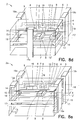
- Figs. 7a and 7b illustrate a side view of a cross-section and a top view of a cross-section, respectively, of a BAW filter that is constructed in accordance with the invention, wherein the cross-sectional view of Fig. 7a is taken along line 7a-7a of Fig. 7b, and wherein in Fig. 7b the upper acoustic mirror and protective layer are removed.
- Fig. 7c illustrates a top view of a cross-section of a BAW filter that is constructed in accordance with another embodiment of the invention, wherein in Fig. 7c the upper acoustic mirror and protective layer are removed, wherein a side view of another cross-section of the BAW filter is represented by Fig. 7a, and wherein the cross-sectional view of Fig. 7a is taken along line 7a-7a of Fig. 7c.
- Fig. 7d illustrates a schematic diagram of the BAW filter of Figs. 7a and 7b.
- Fig. 7e illustrates a schematic diagram of the BAW filter of Figs. 7a and 7c.
- Figs. 8a and 8b illustrate a side view of a cross-section and a top view of a cross-section, respectively, of a BAW filter that is constructed in accordance with another embodiment of the invention, wherein the cross-sectional view of Fig. 8a is taken along line 8a-8a of Fig. 8b, and wherein in Fig. 8b the upper acoustic mirror and protective layer are removed.
- Fig. 8c illustrates a top view of a cross-section of a BAW filter that is constructed in accordance with another embodiment of the invention, wherein in Fig. 8c the upper acoustic mirror and protective layer are removed, wherein a side view of a cross-section of the BAW filter is represented by Fig. 8a, and wherein the cross-sectional view of Fig. 8a is taken along line 8a-8a of Fig. 8c.
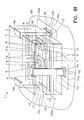
- Fig. 8d shows a perspective view of the BAW filter of Figs. 8a and 8b.
- Fig. 8e shows a perspective view of the BAW filter of Figs. 8a and 8c.
- Fig. 8f illustrates the BAW filter of Fig. 8d surface mounted on a circuit board.
- Fig. 8g illustrates the BAW filter of Fig. 8e surface mounted on a circuit board.
- Fig. 9 illustrates a logic flow diagram of a method in accordance with the invention.
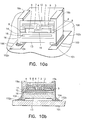
- Fig. 10a illustrates a cross section of a BAW filter of the invention surface mounted on a circuit board.
- Fig. 10b illustrates a front view the cross section of the BAW filter of Fig. 10a surface mounted on a circuit board.
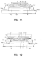
- Fig. 11 shows the BAW filter of Fig. 7a coupled to contacts of a circuit board by bonding wires.
- Fig. 12 shows the BAW filter of Fig. 7a, after having been coupled to contacts of a circuit board using flip-chip technology.
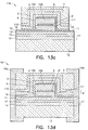
- Fig. 13a is a cross-section of a Stacked Crystal Filter (SCF) that is constructed in accordance with an embodiment of the invention, wherein a top portion of the SCF includes an acoustic mirror.
- SCF Stacked Crystal Filter
- Fig. 13b shows a top view of a portion of the SCF of Fig. 13a, with the acoustic mirror removed.
- Fig. 13c shows a cross-section of the Stacked Crystal Filter of Fig. 13a, taken along lines 13c-13c of Fig. 13a.
- Fig. 13d shows a cross-section of a Stacked Crystal Filter that is constructed in accordance with another embodiment of the invention.
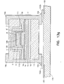
- Fig. 13e shows the Stacked Crystal Filter of Fig. 13c coupled to contacts of a circuit board by bonding wires.
- Fig. 13f shows the Stacked Crystal Filter of Fig. 13c, after having been coupled to contacts of a circuit board using flip-chip technology.
- Fig. 13g shows the Stacked Crystal Filter of Fig. 13d surface mounted on a circuit board.
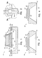
- a cross-section (side view) and a top view, respectively, are shown of a BAW resonator 20 having a membrane or bridge structure 28.
- the BAW resonator 20 comprises a piezoelectric layer 22, a first protective layer 38b, a second protective layer 38a, a first electrode 24, a second electrode 26, the membrane 28, etch windows 40a and 40b, an air gap 34, and a substrate 36.
- the piezoelectric layer 22 comprises, by example, a piezoelectric material that can be fabricated as a thin film such as, by example, zinc-oxide (ZnO), or aluminum-nitride (AIN).
- the membrane 28 comprises two layers, namely, a top layer 30 and a bottom layer 32.
- the top layer 30 is comprised of, by example, poly-silicon (poly-si) or aluminum-nitride (AIN), and the bottom layer 32 is comprised of, by example, silicon-dioxide (SiO 2 ) or gallium arsenide (GaAs).
- the substrate 36 is comprised of a material such as, by example, silicon (Si), SiO 2 , GaAs, or glass. Through the etch windows 40a and 40b, a portion of the substrate 36 is etched to form the air gap 34 after the membrane layers have been deposited over the substrate 36.
- a BAW resonator 21 is shown.
- the BAW resonator 21 is similar to the one illustrated in Fig. 1, with an addition of a sacrificial layer 39.
- the sacrificial layer 39 is deposited over the substrate 36 prior to the deposition of the membrane 28. After all of the resonator layers are formed, the sacrificial layer 39 is removed through the etch windows 40a and 40b to form air gap 34.
- the piezoelectric layer 22 produces vibrations in response to a voltage being applied across the electrodes 24 and 26.
- the vibrations that reach the interface between the membrane 28 and the air gap 34 are reflected by this interface back into the membrane 28. In this manner, the air gap 34 isolates vibrations produced by the piezoelectric layer 22 from the substrate 36.
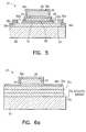
- FIG. 6a another BAW resonator 23 is shown.
- This resonator 23 has a similar structure as that of the BAW resonator 21 of Fig. 1, except that only a single protective layer 38a is provided, and the membrane 28 and the air gap 34 are replaced with an acoustic mirror 70 which acoustically isolates vibrations produced by the piezoelectric layer 22 from the substrate 36.
- the acoustic mirror 70 preferably comprises an odd number of layers (e.g., from three to nine layers).
- the acoustic mirror 70 shown in Fig. 6a comprises three layers, namely a top layer 70a, a middle layer 70b, and a bottom layer 70c.
- Each layer 70a, 70b and 70c has a thickness that is, by example, approximately equal to one quarter wavelength.
- the top layer 70a and bottom layer 70c are comprised of materials having low acoustic impedances such as, by example, silicon (Si), poly-silicon, aluminum (Al), or a polymer.
- the middle layer 70b is comprised of a material having a high acoustic impedance such as, by example, gold (Au), molybdenum (Mo), or tungsten (W).
- a ratio of the acoustic impedances of consecutive layers is large enough to permit the impedance of the substrate to be transformed to a lower value.
- the substrate 36 may be comprised of various high acoustic impedance materials or low acoustic impedance materials (e.g., Si, SiO 2 , GaAs, glass, or a ceramic material).
- Fig. 6b shows an exemplary structure 71 that models layers of an acoustic mirror.
- the structure 71 includes a number of sets of high and low impedance transmission lines L 1 , L 2 , L 3 ...L n-1 and L n that have impedances representing those of acoustic mirror layers. Each transmission line is one-quarter wavelength long.
- the sets of transmission lines L 1 and L 3 have low impedances and represent, by example, the bottom layer 70c and the top layer 70a, respectively, or vice versa, of the acoustic mirror 70.
- the transmission lines of set L 2 have high impedances and represent, by example, the middle layer 70b of the acoustic mirror 70.
- a load impedance Z 2 is also shown which represents the impedance of the substrate 36.
- Transmission lines of set L n-1 and L n are also included in Fig. 6b, and represent layers for a case in which more than three layers are included within the acoustic mirror 70.
- the label "n" represents an even number.
- a ratio of the acoustic impedances of adjacent sets of transmissions lines is large enough to transform the load impedance Z 2 to a minimum impedance Z 1 , which represents an impedance at an interface between the electrode 24 and the top layer 70a of the acoustic mirror 70. In a case in which this ratio is small, however, additional layers are needed to transform the load impedance Z 2 to a minimum impedance.
- the piezoelectric layer 22 vibrates, the vibrations it produces are substantially isolated from the substrate 36 by the interface between the electrode 24 and the top layer 70a.
- the acoustic mirror 70 preferably comprises an odd number of layers, an even number of layers can also be employed in certain cases.
- one or more adhesive layers may be employed between the bottom electrode 24 and the top layer 70a, and/or between the substrate 36 and the bottom layer 70c, in order to securely adhere these layers to one another.
- the adhesive layers may be formed of any suitable adhesive material.
- the particular adhesive material used in the device depends on various factors such as, for example, the thicknesses of the layers surrounding the adhesive layers, the types of materials included within the surrounding layers, the type of deposition process used to fabricate the surrounding layers, and the environmental conditions (e.g., temperature) present during the deposition of the piezoelectric layer 22.
- a cross-section of another type of BAW resonator 80 is shown.
- the resonator 80 comprises a piezoelectric layer 82, a top electrode 84, a bottom electrode 86, a membrane 88, and a substrate 90 having a via 92.
- the resonator 80 functions in a similar manner as the resonator 20 described above in that both of these devices employ air interfaces to reflect acoustic vibrations produced by the piezoelectric layers 22 and 82 of the respective devices.
- a primary difference between these resonators 20 and 80 is the method employed for fabricating the respective air interfaces. For example, for the resonator 80, after all of the layers 84, 86, 82, and 88 are formed, a portion of the substrate is then etched away from underneath the substrate 90 to form the via 92.
- Fig. 4 illustrates another type of resonator 80'which comprises a top electrode 84', a piezoelectric layer 82', a bottom electrode 86', and a substrate 90'that includes a via 92' and a membrane 88'.
- the membrane 88' is formed by removing some material from underneath the substrate 90'.
- the resonator 80' functions like the resonator 80 of Fig. 3.
- At least some of the layers that form the resonators described above may be exposed to the air.
- the inventor has developed a novel and inexpensive technique for protecting layer surfaces of BAW filters.
- the technique avoids the high costs of using presently-available techniques for protecting exposed resonator layer surfaces from becoming contaminated or otherwise damaged.
- the technique also permits BAW filters to be fabricated in a manner so as to provide interfaces for reflecting acoustic waves that replace the air interfaces of known types of BAW resonators.
- Fig. 7b illustrates a top view of a Bulk Acoustic Wave (BAW) filter 1 that is constructed in accordance with the invention
- Fig. 7a which represents a side view of a cross-section of the filter 1 taken along line 7a-7a of Fig. 7b.
- the BAW filter 1 comprises a substrate 13, a first acoustic mirror 17 that is situated atop the substrate 13, a first resonator 7, and a second resonator 12.
- the first and second resonators 7 and 12 are situated over the first acoustic mirror 17.
- a second acoustic mirror 18 is disposed over the first and second resonators 7 and 12.
- the second acoustic mirror 18 can be disposed over a portion of the first acoustic mirror 17, although this is not shown in Figs. 7a or 7b.
- a protective passivation layer 3 is disposed over the second acoustic mirror 18.
- the first, lower acoustic mirror 17 comprises three layers, namely a top layer 14, a middle layer 15, and a bottom layer 16.
- Each layer 14, 15, and 16 has a thickness that is, by example, approximately equal to one quarter wavelength at the resonant frequency of the BAW filter 1.
- the top layer 14 and bottom layer 16 are comprised of materials having low acoustic impedances such as, by example, silicon (Si), poly-silicon, aluminum (Al), or a polymer.
- the middle layer 15 is comprised of a material having a high acoustic impedance such as, by example, gold (Au), molybdenum (Mo), or tungsten (W).
- the acoustic impedance of the middle layer 15 is greater than the acoustic impedance of the top layer 14.
- the acoustic impedance of the middle layer 15 is greater than the acoustic impedance of the bottom layer 16.
- a ratio of the acoustic impedance of layer 15 to that of layer 14, and a ratio of the acoustic impedance of the layer 15 to that of layer 16 are large enough to permit the impedance of the substrate 13 to be transformed to a lower value.
- first acoustic mirror 17 may be provided within the first acoustic mirror 17 to transform this impedance to the lower value.
- the adhesive layers may include any suitable adhesive material, depending on various factors such as, for example, the thicknesses of the layers surrounding the adhesive layers, the types of materials included within the surrounding layers, the type of deposition process used to fabricate the surrounding layers, and the environmental conditions (e.g., temperature) present during the deposition of the piezoelectric layer 22.
- the resonator layers become securely adhered to one another after being deposited such that no adhesive layers need to be employed.
- the vibrations it produces are substantially isolated from the substrate 13 by the first acoustic mirror 17.
- the substrate 13 may be comprised of various low impedance materials such as, by example, Si, SiO 2 , GaAs, glass, or a ceramic material. However, owing to the impedance transformation that occurs via the layers 14, 15 and 16 of the first acoustic mirror 17, the substrate 13 may also be comprised of high impedance materials.
- the second, upper or top acoustic mirror 18 also comprises three layers, namely a top layer 4, a middle layer 5, and a bottom layer 6. Each of these layers has a thickness that is, by example, approximately equal to one-quarter wavelength.
- the top layer 4 and the bottom layer 6 are preferably comprised of materials having low acoustic impedances, such as, by example, silicon (Si), poly-silicon, aluminum (Al), or a polymer.
- the middle layer 5 is preferably comprised of a material having a high acoustic impedance such as, by example, gold (Au), molybdenum (Mo), or tungsten (W).
- the protective passivation layer 3 which protects a top portion of the BAW filter 1, has a thickness of 0.2 ⁇ m or greater.
- the protective passivation layer 3 may be comprised of any suitable protective material such as, by example, epoxy, SiO 2 , or a glop top material (e.g., an epoxy-based viscous fluid which hardens after being heated). It should be recognized that the use of three layers in the second acoustic mirror 18 is exemplary, and that a greater odd number of layers could be used, as was previously described. Also, one or more adhesive layers may be employed if needed to securely adhere the bottom layer 6 to top surfaces of resonators 7 and 12, and/or to securely adhere the top layer 4 to the protective passivation layer 3.
- the first and second resonators 7 and 12 are BAW resonators. Each of these resonators 7 and 12 includes (1) a respective portion of a bottom electrode 19 that is situated over the first acoustic mirror 17, (2) a piezoelectric layer 9 that is situated over the respective portion of the bottom electrode 19 and over a respective portion of the first acoustic mirror 17, and (3) a top electrode 8 that is formed over portions of the piezoelectric layer 9 and over a respective portion of the first acoustic mirror 17. A portion of the top electrode 8 of the first resonator 7 is not covered by the second acoustic mirror 18 or the protective passivation layer 3, and is exposed for providing a first contact pad 10.
- top electrode 8 of the second resonator 12 is not covered by the second acoustic mirror 18 or the protective passivation layer 3, and is exposed for providing a second contact pad 11. Also, referring to Fig. 7b, another portion of this top electrode 8 of resonator 12 forms a top electrode of a resonator 12', which will be described below.
- the contact pads 10 and 11 of the BAW filter 1 provide an input and an output respectively for the filter 1.
- the contact pads 10 and 11 permit the BAW filter 1 to be electrically coupled to an external circuit by wire or solder bonding, or by another suitable technique.
- contact pads 10 and 11 can be coupled to respective contact pads 102a and 102b of a circuit board 106 via bonding wires 112.
- contact pads 10 and 11 can be coupled to contact pads 102a and 102b of circuit board 106 via solder bumps 114, using flip-chip technology.
- the filter 1 also includes third and fourth resonators 7' and 12', respectively, in addition to the first and second resonators 7 and 12.
- the third and fourth resonators 7'and 12' are constructed of similar components as the resonators 7 and 12.
- a ground contact pad (G) is connected to top electrode 8 of the third resonator 7', and is not covered by the second acoustic mirror 18 or the protective passivation layer 3.
- the ground contact pad (G) is also coupled to a portion of bottom electrode 19 of the fourth resonator 12'.
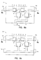
- the filter 1 has a ladder topology.
- a schematic diagram of the filter 1 is shown in Fig. 7d.
- Fig. 7c shows a top view of a cross-section of a filter 1a that is constructed in accordance with another embodiment of the invention.
- the filter 1a is constructed of similar components as the filter 1 shown in Fig. 7b, except that two ground contact pads (G1) and (G2) are provided instead of only a single ground contact pad (G).
- the ground contact pads (G1) and (G2) are not covered by the second acoustic mirror 18 or the protective passivation layer 3. Both of the ground contact pads (G1) and (G2) are coupled to the top electrode 8 of the resonator 7' and to the bottom electrode 19 of the resonator 12'.
- a schematic diagram of the filter 1a is shown in Fig. 7e.
- Figs. 8a and 8b illustrate a side view of a cross-section and a top view of a cross-section, respectively, of a BAW filter 2 that is constructed in accordance with another embodiment of the invention.
- the BAW filter 2 of Figs. 8a and 8b is formed of similar layers as the BAW filter 1 of Figs. 7a and 7b.
- the portions of the electrodes which formed the contact pads 10,11, and (G) of Figs. 7a and 7b are fully covered by the second acoustic mirror 18 (although this is not shown for resonators 7' and 12').
- the BAW filter 2 does, however, include contacts 19a, 19b, and 19c (i.e., electrodes) that are disposed over external surfaces of the BAW filter 2.
- Fig. 8d shows a perspective view of the BAW filter 2, with the top acoustic mirror 18 and the protective layer 3 removed from the area of the filter 2 including the resonators 7' and 12'(only the piezoelectric layers 9 and the top and bottom electrodes 8 and 19, respectively, of the resonators 7' and 12' are shown in Fig. 8d).
- Contacts 19a and 19b are disposed over opposite external surfaces of the BAW filter 2, and contact 19c is disposed over another external surface of the BAW filter 2.
- Contacts 19a and 19b are situated adjacent to respective portions of the protective passivation layer 3, the first and second acoustic mirrors 17 and 18, the substrate 13, and to a portion of the electrode 8 of a respective one of the resonators 7 and 12.
- Contact 19a is electrically coupled to the top electrode 8 of the first resonator 7, and contact 19b is electrically coupled to the top electrode 8 of the second resonator 12.
- Contact 19c is situated adjacent to respective portions of the protective passivation layer 3, the first and second acoustic mirrors 17 and 18, and the substrate 13, and is electrically coupled to the top electrode 8 of the third resonator 7' and to the bottom electrode 19 of the fourth resonator 12'.
- Each contact 19a, 19b, and 19c is comprised of an electrically conductive material such as, by example, gold (Au).
- Au gold
- the placement of the contacts 19a, 19b, and 19c enable the BAW filter 2 to be attached to a circuit board by surface mounting techniques, thereby simplifying circuit assembly.
- the BAW filter 2 can be surface mounted on a circuit board 106 by soldering the contacts 19a, 19b, and 19c to respective contact pads 102a, 102b, and 102c of the circuit board 106. This enables the contacts 19a, 19b, and 19c to be electrically coupled to circuit board wiring 100.
- Fig. 8c shows a top view of a cross-section of a BAW filter 2a that is constructed in accordance with another embodiment of the invention.
- a side view of a cross-section of the BAW filter 2a taken along line 8a-8a of Fig. 8c is represented by Fig. 8a.
- the BAW filter 2a is formed of similar layers as the BAW filter 1a of Figs. 7a and 7c.
- Fig. 8e shows a perspective view of the BAW filter 2a, with the top acoustic mirror 18 and the protective layer 3 removed from the area of the filter 2a including the resonators 7' and 12'.
- the BAW filter 2a includes contacts 19a and 19b, which are similar to those described above, and also includes contacts 19d and 19e.
- contacts 19a and 19b are disposed over opposite external surfaces of the filter 2a, and contacts 19d and 19e are also disposed over opposite external surfaces of the filter 2a.
- the contacts 19a, 19b, 19d, and 19e are comprised of an electrically conductive material such as, by example, gold (Au).
- Contact 19a is electrically coupled to the top electrode 8 of the first resonator 7, and contact 19b is electrically coupled to the top electrode 8 of the second resonator 12.
- each of the contacts 19d and 19e is electrically coupled to the top electrode 8 of the third resonator 7' and to the bottom electrode 19 of the fourth resonator 12'.
- the contacts 19a, 19b, 19d, and 19e enable the BAW filter 2 to be electrically coupled to an external circuit.
- the placement of the contacts 19a, 19b, 19d, and 19e enable the BAW filter 2a to be attached to a circuit board by surface mounting techniques, thereby simplifying circuit assembly.
- the BAW filter 2a can be surface mounted on a circuit board 106 by soldering the contacts 19a, 19b, 19d, and 19e to respective contact pads 102a, 102b, 102d, and 102e of the circuit board 106.
- the contacts 19a, 19b, 19d, and 19e further serve to at least partially isolate the BAW filter 2a from environmental contaminants such as, by example, solder 104 or solvents, that may be encountered during assembly and subsequent use.
- Figs. 13a-13c illustrate various views of another embodiment of the invention, namely a BAW filter 116 having a stacked filter structure.
- the filter 116 is also referred to as a "Stacked Crystal Filter” (SCF) 116.
- SCFs are two part devices and exhibit only a series resonance.
- the SCF 116 includes a substrate 13, a first, bottom acoustic mirror 17, a second, top acoustic mirror 18, and a protective passivation layer 3, which are similar to those described above.
- the SCF 116 also comprises a first, bottom resonator 111, and a second, top resonator 109.
- the bottom resonator 111 is disposed over the bottom acoustic mirror 17.
- the top resonator 109 is disposed over the first resonator 111, thereby forming a resonator stack.
- the first, bottom resonator 111 includes a piezoelectric layer 110, a lower electrode 19, and a ground electrode 8'.
- the piezoelectric layer 110 is located between portions of the ground electrode 8' and the electrode 19.
- the second, top resonator 109 includes the ground electrode 8', a piezoelectric layer 108, and an upper electrode 8.
- the piezoelectric layer 108 is disposed between portions of the ground electrode 8' and the upper electrode 8.
- the piezoelectric layers 108 and 110 and the electrodes 8, 8', and 19 comprise similar materials and may have similar thicknesses as those described above.
- the second acoustic mirror 18 covers the resonator stack and portions of the first acoustic mirror 17.
- a portion of the ground electrode 8' is not covered by the second acoustic mirror 18 or the protective passivation layer 3, and is exposed for providing a ground contact pad 8".
- portions of the upper and lower electrodes 8 and 19, respectively are not covered by the second acoustic mirror 18 or by the protective passivation layer 3, and are exposed for providing first and second contact pads 10 and 11, respectively.
- the contact pads 8", 10 and 11 permit the SCF 116 to be electrically coupled to an external circuit by wire or solder bonding, or by another suitable technique.
- contact pads 10 and 11 can be coupled to respective contact pads 102a and 102b of a circuit board 106 via bonding wires 112.
- contact pads 10 and 11 can be coupled to contact pads 102a and 102b of circuit board 106 via solder bumps 114, using flip-chip technology. It should be noted that, although not shown in Figs. 13e and 13f, the contact pad 8" of the SCF 116 can also be coupled to the circuit board 106 using these techniques.
- Fig. 13d illustrates a cross-section of a SCF 118 that is constructed in accordance with another embodiment of the invention.
- the SCF 118 has a similar structure as the SCF 116 of Figs. 13a-13c. However, in this embodiment of the invention, the portions of the electrodes 8, 8', and 19 that formed the contact pads 10, 8", and 11 of the SCF 116 are fully covered by the second acoustic mirror 18. As such, no exposed contact pads 10, 8", and 11 are provided.
- the SCF 118 does, however, include contacts 19a and 19b (i.e., electrodes) that are disposed over opposite external surfaces of the SCF 118.
- Each contact 19a and 19b is situated adjacent to respective portions of the protective passivation layer 3, the first and second acoustic mirrors 17 and 18, the substrate 13, and to respective portions of the electrodes 8 and 19.
- Each contact 19a and 19b is constructed of, by example gold (Au).
- Contact 19a is electrically coupled to the lower electrode 19 and contact 19b is electrically coupled to upper electrode 8.
- the contacts 19a and 19b enable the SCF 118 to be electrically coupled to an external circuit.
- the contacts 19a and 19b enable the SCF to be surface mounted to a circuit board 106.
- the contacts 19a and 19b may be soldering the contacts 19a and 19b to respective contact pads 102a and 102 of the circuit board 106, thereby enabling the contacts 19a and 19b to be electrically coupled to circuit board wiring 100.
- the contacts 19a and 19b further serve to at least partially isolate the SCF 118 from environmental contaminants such as, for example, solder 104 or solvents, that may be encountered during assembly and subsequent use.
- the BAW filters 1, 1a, 2, and 2a, and the SCFs 116 and 118 described above may comprise more or less than the number of piezoelectric layers and electrodes described above, depending on filter performance requirements for a particular application of interest.
- the first and second acoustic mirrors 17 and 18 of these devices may each comprise more than three layers.
- the first and second acoustic mirrors 17 and 18 may each comprise an additional two, four, six, or more layers, as long as the total number of layers employed are arranged such that consecutive ones of these layers have alternating high and low impedances.
- top and bottom acoustic mirrors 17 and 18 may be employed if needed for securely adhering the top and bottom acoustic mirrors 17 and 18 to respective portions of the filter structures.
- topologies of the BAW filters 1, 1a, 2, and 2a described above is not intended to be limiting to the scope of the invention, and that other topologies may be provided.
- the BAW filters 1, 1a, 2, and 2a may include more or less than the number of resonators, contact pads, and/or external contacts described above.
- a second (i.e., top) acoustic mirror offers a number of advantages over devices that only include a single acoustic mirror, such as the one shown in Fig. 6.
- One advantage of employing a second acoustic mirror can be appreciated in view of the following description.
- acoustic waves propagate from each vibrating piezoelectric layer within these filters in a direction that is towards the first, lower acoustic mirror 17 of the respective filters.
- the first acoustic mirror 17 reflects at least portions of these acoustic vibrations in a direction that is not towards the substrate 13.
- the reflected portions of the acoustic waves do not reach the substrate 13.
- the first acoustic mirror 17 isolates the vibrations produced by the vibrating piezoelectric layers from the substrate 13 within the respective filters 1, 1a, 2, 2a, 116, and 118.
- Acoustic waves also propagate from each vibrating piezoelectric layer in a direction that is towards the second acoustic mirror 18.
- the second acoustic mirror 18 functions in a similar manner as the first acoustic mirror 17. More particularly, owing at least in part of the impedances of the layers 4, 5 and 6 that form the second acoustic mirror 18, the second acoustic mirror 18 reflects the acoustic vibrations in a direction that is not towards the protective passivation layer 3, nor in a direction that is towards the external contacts (e.g., 19a and 19b) for a case in which the BAW filter 2, the BAW filter 2a, or the SCF 118 is employed.
- the reflected acoustic waves do not reach these portions of the respective devices, and hence do not reach the interface between the second acoustic mirror 18 and the protective passivation layer 3.
- the second acoustic mirror 18 prevents the reflected acoustic waves from reaching the interfaces between the second acoustic mirror 18 and portions of the contacts (e.g., contacts 19a and 19b) located in the upper portion of the respective devices.
- the reflected portions of the acoustic waves do not reach the material.
- the second acoustic mirror 18 isolates this material from acoustic vibrations produced by the piezoelectric layers.
- the second acoustic mirror 18 covers substantially all of the resonators 7, 12, 7', and 12' of the BAW filters 1, 1a, 2, and 2a, and substantially all of the resonators 109 and 111 of the SCFs 116 and 118, and thus prevents solvents and the like from coming into contact with, and contaminating or otherwise harming, the layers of these devices.
- the second acoustic mirror 18 protects these layers in this manner, there is no need to provide other forms of protection for these layers, such as, by example, semi-hermetic packaging. Thus, costs associated with these other forms of protection are avoided, and the overall costs of fabricating the devices are considerably reduced.
- the invention employs BAW filters instead of SAW resonator filters
- protective packaging is not required to protect the BAW filters
- the BAW filters of the present invention can exhibit smaller parasitic components (e.g., parasitic capacitances) than filters (e.g., SAW filters) that require protective packaging.
- the overall sizes of these individual devices can be smaller than, for example, individual semi-hermetically packaged filters.
- the second acoustic mirror is employed within BAW filters instead of within SAW filters, which require some form of hermetic packaging for protection.
- the acoustic mirror would need to include inter-digital metallization patterns disposed on a surface of the devices, as acoustic waves propagate within SAW filters in a direction that is parallel to the layer surfaces of the filters.
- inter-digital metallization patterns necessitates the use of hermetic packaged for protection in these SAW devices.
- a method for fabricating a BAW filter and assembling the filter on a circuit board.
- the method includes a step (A) of forming a first, lower acoustic mirror over a substrate.
- a next step (B) includes forming at least one resonator on the lower acoustic mirror.
- the at least one resonator may include one or more BAW resonators that are similar to those described above.
- two or more resonators may be formed adjacent to one another on a top surface of the lower acoustic mirror.
- a stack of resonators may be formed on the top surface of the lower acoustic mirror to form a stacked crystal structure.
- Contact pads may also be formed from portions of the resonator electrodes to provide input, output, and grounding pads.
- a second, upper acoustic mirror is formed over at least a substantial portion of the at least one resonator.
- the upper acoustic mirror may also be formed over other portions of the filter including, by example, a portion of the lower acoustic mirror.
- the step (C) includes the steps of forming a first, lower layer over the at least one resonator and over a portion of the lower acoustic mirror, forming a second, middle layer over the lower layer, and forming a third, upper layer over the middle layer.
- the lower, middle, and upper layers form the upper acoustic mirror which is similar to that described above.
- the lower and upper layers include a material having a low acoustic impedance such as silicon, poly-silicon, aluminum, or a polymer material.
- the middle layer includes a material having a high acoustic impedance such as gold, molybdenum, or tungsten.
- the method further includes the steps of (D) forming a protective passivation layer over the upper layer of the upper acoustic mirror, and patterning the layers formed in steps (C) and (D) to create openings for the contact pads, if any are provided.
- the protective passivation layer and the contact pads are also similar to those described above.
- the upper acoustic mirror protects the resonator from being contacted by external materials that can harm the at least one resonator.
- more than one BAW filter may be fabricated on a wafer in accordance with these method steps.
- step (F1) the wafer is cut into chips.
- step (F2) the chips are coupled to circuitry of a circuit board with bonding wires.
- step (G1) solder bumps are fabricated on contact pads of the filter using, by example, vacuum deposition (e.g., evaporation) of a bump metal or electrochemical plating of solder.
- step (G2) the chips, are coupled to selected contacts of the circuit board using flip-chip technology.
- steps (H1) and (H2) are performed.
- step (H1) the wafer is cut into chips and contacts are formed over portions of the filter. These contacts are similar to the contacts (e.g., contacts 19a and 19b) described above, and can be fabricated using, for example, a silver dipping technique similar to that used to fabricate terminations for conventional surface mount discrete components.
- step (H2) the chips are coupled to selected circuit board contact pads using surface mount technology.
- the upper acoustic mirror protects the at least one resonator from being contacted by external materials that can harm the resonator.
Landscapes
- Physics & Mathematics (AREA)
- Acoustics & Sound (AREA)
- Chemical & Material Sciences (AREA)
- Crystallography & Structural Chemistry (AREA)
- Engineering & Computer Science (AREA)
- Manufacturing & Machinery (AREA)
- Piezo-Electric Or Mechanical Vibrators, Or Delay Or Filter Circuits (AREA)
- Transducers For Ultrasonic Waves (AREA)
Applications Claiming Priority (2)
| Application Number | Priority Date | Filing Date | Title |
|---|---|---|---|
| US816702 | 1977-07-18 | ||
| US08/816,702 US5872493A (en) | 1997-03-13 | 1997-03-13 | Bulk acoustic wave (BAW) filter having a top portion that includes a protective acoustic mirror |
Publications (3)
| Publication Number | Publication Date |
|---|---|
| EP0865157A2 true EP0865157A2 (de) | 1998-09-16 |
| EP0865157A3 EP0865157A3 (de) | 2000-04-05 |
| EP0865157B1 EP0865157B1 (de) | 2009-04-29 |
Family
ID=25221393
Family Applications (1)
| Application Number | Title | Priority Date | Filing Date |
|---|---|---|---|
| EP98301934A Expired - Lifetime EP0865157B1 (de) | 1997-03-13 | 1998-03-13 | Akustisches Volumenwellenfilter |
Country Status (4)
| Country | Link |
|---|---|
| US (1) | US5872493A (de) |
| EP (1) | EP0865157B1 (de) |
| JP (1) | JP4212137B2 (de) |
| DE (1) | DE69840784D1 (de) |
Cited By (18)
| Publication number | Priority date | Publication date | Assignee | Title |
|---|---|---|---|---|
| EP1067685A3 (de) * | 1999-07-07 | 2001-06-27 | Philips Corporate Intellectual Property GmbH | Volumenwellen-Filter |
| DE10007577C1 (de) * | 2000-02-18 | 2001-09-13 | Infineon Technologies Ag | Piezoresonator |
| US6388544B1 (en) | 1999-11-29 | 2002-05-14 | Nokia Mobile Phones Ltd. | Method for adjusting the center frequency of a balanced filter and a plurality of balanced filters |
| EP1017170A3 (de) * | 1998-12-30 | 2003-01-02 | Nokia Corporation | Gegentakt Filterstruktur |
| WO2003043188A1 (de) * | 2001-11-14 | 2003-05-22 | Infineon Technologies Ag | Passivierter baw-resonator und baw-filter |
| EP1187318A3 (de) * | 2000-09-11 | 2003-05-28 | Agilent Technologies, Inc. (a Delaware corporation) | Akustischer Resonator |
| GB2391408A (en) * | 2002-07-30 | 2004-02-04 | Agilent Technologies Inc | FBAR thin-film resonator with protective layer |
| WO2004021568A1 (de) * | 2002-08-27 | 2004-03-11 | Epcos Ag | Resonator und bauelement mit hermetischer verkapselung |
| EP1227581A3 (de) * | 2001-01-16 | 2004-12-15 | Nokia Corporation | Akustischer Vollumenwellenresonator mit einem leitenden akustischen Spiegel |
| US7145417B2 (en) | 2002-03-29 | 2006-12-05 | Fujitsu Limited | Filter chip and filter device |
| US7187254B2 (en) | 2000-11-29 | 2007-03-06 | Tdk Corporation | Film bulk acoustic resonator filters with a coplanar waveguide |
| GB2422969B (en) * | 2003-10-30 | 2007-04-11 | Agilent Technologies Inc | Film bulk acoustic resonator (fbar) devices with simplified packaging |
| US7362198B2 (en) | 2003-10-30 | 2008-04-22 | Avago Technologies Wireless Ip (Singapore) Pte. Ltd | Pass bandwidth control in decoupled stacked bulk acoustic resonator devices |
| EP1120910B1 (de) * | 2000-01-18 | 2009-03-18 | Texas Instruments Incorporated | Akustische Mehrfrequenzreflektoranordnung und Verfahren |
| EP1309084A4 (de) * | 2001-06-11 | 2009-11-04 | Panasonic Corp | Piezoelektrischer vibrator und filter der denselben verwendet |
| USRE42009E1 (en) | 2003-09-17 | 2010-12-28 | Panasonic Corporation | Piezoelectric resonator having a spurious component control layer, filter using the piezoelectric resonator, and duplexer using the piezoelectric resonator |
| US9859205B2 (en) | 2011-01-31 | 2018-01-02 | Avago Technologies General Ip (Singapore) Pte. Ltd. | Semiconductor device having an airbridge and method of fabricating the same |
| WO2024072949A1 (en) * | 2022-09-30 | 2024-04-04 | Texas Instruments Incorporated | Radiator layers for ultrasonic transducers |
Families Citing this family (210)
| Publication number | Priority date | Publication date | Assignee | Title |
|---|---|---|---|---|
| US6087198A (en) * | 1998-02-12 | 2000-07-11 | Texas Instruments Incorporated | Low cost packaging for thin-film resonators and thin-film resonator-based filters |
| US6081171A (en) * | 1998-04-08 | 2000-06-27 | Nokia Mobile Phones Limited | Monolithic filters utilizing thin film bulk acoustic wave devices and minimum passive components for controlling the shape and width of a passband response |
| FI108583B (fi) | 1998-06-02 | 2002-02-15 | Nokia Corp | Resonaattorirakenteita |
| FI106894B (fi) | 1998-06-02 | 2001-04-30 | Nokia Mobile Phones Ltd | Resonaattorirakenteita |
| US5942958A (en) * | 1998-07-27 | 1999-08-24 | Tfr Technologies, Inc. | Symmetrical piezoelectric resonator filter |
| JP2000209063A (ja) * | 1998-11-12 | 2000-07-28 | Mitsubishi Electric Corp | 薄膜圧電素子 |
| US6262637B1 (en) * | 1999-06-02 | 2001-07-17 | Agilent Technologies, Inc. | Duplexer incorporating thin-film bulk acoustic resonators (FBARs) |
| DE19947081A1 (de) * | 1999-09-30 | 2001-04-05 | Infineon Technologies Ag | Akustischer Spiegel und Verfahren zu dessen Herstellung |
| US6339276B1 (en) * | 1999-11-01 | 2002-01-15 | Agere Systems Guardian Corp. | Incremental tuning process for electrical resonators based on mechanical motion |
| US6466107B2 (en) * | 1999-12-14 | 2002-10-15 | Murata Manufacturing Co., Ltd. | Ladder filter comprising stacked piezoelectric resonators |
| US6746577B1 (en) | 1999-12-16 | 2004-06-08 | Agere Systems, Inc. | Method and apparatus for thickness control and reproducibility of dielectric film deposition |
| US6524971B1 (en) | 1999-12-17 | 2003-02-25 | Agere Systems, Inc. | Method of deposition of films |
| US6323744B1 (en) * | 2000-02-04 | 2001-11-27 | Agere Systems Guardian Corp. | Grounding of TFR ladder filters |
| US6306313B1 (en) | 2000-02-04 | 2001-10-23 | Agere Systems Guardian Corp. | Selective etching of thin films |
| US6437667B1 (en) | 2000-02-04 | 2002-08-20 | Agere Systems Guardian Corp. | Method of tuning thin film resonator filters by removing or adding piezoelectric material |
| US7296329B1 (en) | 2000-02-04 | 2007-11-20 | Agere Systems Inc. | Method of isolation for acoustic resonator device |
| US6377136B1 (en) * | 2000-02-04 | 2002-04-23 | Agere Systems Guardian Corporation | Thin film resonator filter having at least one component with different resonant frequency sets or electrode capacitance |
| US6392257B1 (en) * | 2000-02-10 | 2002-05-21 | Motorola Inc. | Semiconductor structure, semiconductor device, communicating device, integrated circuit, and process for fabricating the same |
| US6693033B2 (en) | 2000-02-10 | 2004-02-17 | Motorola, Inc. | Method of removing an amorphous oxide from a monocrystalline surface |
| DE60139444D1 (de) * | 2000-02-22 | 2009-09-17 | Nxp Bv | Verfahren zur herstellung eines auf einem trägersubstrat geformten piezoelektrischen filters mit einem akustischen resonator auf einer akustischen reflektorschicht |
| ATE427583T1 (de) * | 2000-04-06 | 2009-04-15 | Nxp Bv | Abstimmbare filteranordnung |
| WO2001078229A1 (en) * | 2000-04-06 | 2001-10-18 | Koninklijke Philips Electronics N.V. | Tunable filter arrangement comprising resonators. |
| US6603241B1 (en) * | 2000-05-23 | 2003-08-05 | Agere Systems, Inc. | Acoustic mirror materials for acoustic devices |
| KR20030011083A (ko) * | 2000-05-31 | 2003-02-06 | 모토로라 인코포레이티드 | 반도체 디바이스 및 이를 제조하기 위한 방법 |
| GB0014963D0 (en) * | 2000-06-20 | 2000-08-09 | Koninkl Philips Electronics Nv | A bulk acoustic wave device |
| AU2001277001A1 (en) * | 2000-07-24 | 2002-02-05 | Motorola, Inc. | Heterojunction tunneling diodes and process for fabricating same |
| US6555946B1 (en) * | 2000-07-24 | 2003-04-29 | Motorola, Inc. | Acoustic wave device and process for forming the same |
| US6590236B1 (en) | 2000-07-24 | 2003-07-08 | Motorola, Inc. | Semiconductor structure for use with high-frequency signals |
| US6355498B1 (en) | 2000-08-11 | 2002-03-12 | Agere Systems Guartian Corp. | Thin film resonators fabricated on membranes created by front side releasing |
| JP4049239B2 (ja) * | 2000-08-30 | 2008-02-20 | Tdk株式会社 | 表面弾性波素子を含む高周波モジュール部品の製造方法 |
| US6486751B1 (en) | 2000-09-26 | 2002-11-26 | Agere Systems Inc. | Increased bandwidth thin film resonator having a columnar structure |
| US6493497B1 (en) | 2000-09-26 | 2002-12-10 | Motorola, Inc. | Electro-optic structure and process for fabricating same |
| US6638838B1 (en) | 2000-10-02 | 2003-10-28 | Motorola, Inc. | Semiconductor structure including a partially annealed layer and method of forming the same |
| US6674291B1 (en) | 2000-10-30 | 2004-01-06 | Agere Systems Guardian Corp. | Method and apparatus for determining and/or improving high power reliability in thin film resonator devices, and a thin film resonator device resultant therefrom |
| US6587212B1 (en) | 2000-10-31 | 2003-07-01 | Agere Systems Inc. | Method and apparatus for studying vibrational modes of an electro-acoustic device |
| US6501121B1 (en) | 2000-11-15 | 2002-12-31 | Motorola, Inc. | Semiconductor structure |
| US6743731B1 (en) | 2000-11-17 | 2004-06-01 | Agere Systems Inc. | Method for making a radio frequency component and component produced thereby |
| KR100602907B1 (ko) * | 2000-11-27 | 2006-07-20 | 가부시키가이샤 무라타 세이사쿠쇼 | 복합 진동 장치 |
| US6559471B2 (en) | 2000-12-08 | 2003-05-06 | Motorola, Inc. | Quantum well infrared photodetector and method for fabricating same |
| US6550664B2 (en) * | 2000-12-09 | 2003-04-22 | Agilent Technologies, Inc. | Mounting film bulk acoustic resonators in microwave packages using flip chip bonding technology |
| US6496085B2 (en) * | 2001-01-02 | 2002-12-17 | Nokia Mobile Phones Ltd | Solidly mounted multi-resonator bulk acoustic wave filter with a patterned acoustic mirror |
| US6518860B2 (en) * | 2001-01-05 | 2003-02-11 | Nokia Mobile Phones Ltd | BAW filters having different center frequencies on a single substrate and a method for providing same |
| US6424238B1 (en) | 2001-01-08 | 2002-07-23 | Motorola, Inc. | Acoustic wave filter and method of forming the same |
| US20020096683A1 (en) * | 2001-01-19 | 2002-07-25 | Motorola, Inc. | Structure and method for fabricating GaN devices utilizing the formation of a compliant substrate |
| US6515402B2 (en) * | 2001-01-24 | 2003-02-04 | Koninklijke Philips Electronics N.V. | Array of ultrasound transducers |
| US7435613B2 (en) | 2001-02-12 | 2008-10-14 | Agere Systems Inc. | Methods of fabricating a membrane with improved mechanical integrity |
| US6673646B2 (en) | 2001-02-28 | 2004-01-06 | Motorola, Inc. | Growth of compound semiconductor structures on patterned oxide films and process for fabricating same |
| US6483229B2 (en) * | 2001-03-05 | 2002-11-19 | Agilent Technologies, Inc. | Method of providing differential frequency adjusts in a thin film bulk acoustic resonator (FBAR) filter and apparatus embodying the method |
| WO2002082551A1 (en) | 2001-04-02 | 2002-10-17 | Motorola, Inc. | A semiconductor structure exhibiting reduced leakage current |
| WO2002093740A1 (en) * | 2001-05-11 | 2002-11-21 | Ube Electronics, Ltd. | Film bulk acoustic resonator |
| US6709989B2 (en) | 2001-06-21 | 2004-03-23 | Motorola, Inc. | Method for fabricating a semiconductor structure including a metal oxide interface with silicon |
| US6992321B2 (en) | 2001-07-13 | 2006-01-31 | Motorola, Inc. | Structure and method for fabricating semiconductor structures and devices utilizing piezoelectric materials |
| US20030010992A1 (en) * | 2001-07-16 | 2003-01-16 | Motorola, Inc. | Semiconductor structure and method for implementing cross-point switch functionality |
| US6531740B2 (en) | 2001-07-17 | 2003-03-11 | Motorola, Inc. | Integrated impedance matching and stability network |
| US6646293B2 (en) | 2001-07-18 | 2003-11-11 | Motorola, Inc. | Structure for fabricating high electron mobility transistors utilizing the formation of complaint substrates |
| US6693298B2 (en) | 2001-07-20 | 2004-02-17 | Motorola, Inc. | Structure and method for fabricating epitaxial semiconductor on insulator (SOI) structures and devices utilizing the formation of a compliant substrate for materials used to form same |
| US7019332B2 (en) | 2001-07-20 | 2006-03-28 | Freescale Semiconductor, Inc. | Fabrication of a wavelength locker within a semiconductor structure |
| US6855992B2 (en) * | 2001-07-24 | 2005-02-15 | Motorola Inc. | Structure and method for fabricating configurable transistor devices utilizing the formation of a compliant substrate for materials used to form the same |
| US6667196B2 (en) | 2001-07-25 | 2003-12-23 | Motorola, Inc. | Method for real-time monitoring and controlling perovskite oxide film growth and semiconductor structure formed using the method |
| US6594414B2 (en) | 2001-07-25 | 2003-07-15 | Motorola, Inc. | Structure and method of fabrication for an optical switch |
| US6585424B2 (en) | 2001-07-25 | 2003-07-01 | Motorola, Inc. | Structure and method for fabricating an electro-rheological lens |
| US6589856B2 (en) | 2001-08-06 | 2003-07-08 | Motorola, Inc. | Method and apparatus for controlling anti-phase domains in semiconductor structures and devices |
| US6639249B2 (en) | 2001-08-06 | 2003-10-28 | Motorola, Inc. | Structure and method for fabrication for a solid-state lighting device |
| US20030034491A1 (en) | 2001-08-14 | 2003-02-20 | Motorola, Inc. | Structure and method for fabricating semiconductor structures and devices for detecting an object |
| US6673667B2 (en) | 2001-08-15 | 2004-01-06 | Motorola, Inc. | Method for manufacturing a substantially integral monolithic apparatus including a plurality of semiconductor materials |
| US20030036217A1 (en) * | 2001-08-16 | 2003-02-20 | Motorola, Inc. | Microcavity semiconductor laser coupled to a waveguide |
| DE10147075A1 (de) * | 2001-09-25 | 2003-04-30 | Infineon Technologies Ag | Piezoelektrisches Bauelement und Verfahren zu dessen Herstellung |
| US6778038B2 (en) * | 2001-10-05 | 2004-08-17 | Tdk Corporation | Piezoelectric resonant filter, duplexer, and method of manufacturing same |
| DE10149542A1 (de) * | 2001-10-08 | 2003-04-17 | Infineon Technologies Ag | BAW-Resonator |
| DE10150253A1 (de) * | 2001-10-11 | 2003-04-30 | Infineon Technologies Ag | Piezoelektrisches Bauelement |
| US20030071327A1 (en) * | 2001-10-17 | 2003-04-17 | Motorola, Inc. | Method and apparatus utilizing monocrystalline insulator |
| KR20030032401A (ko) * | 2001-10-18 | 2003-04-26 | 한국쌍신전기주식회사 | 압전박막형 공진기 및 그 제조방법 |
| DE60140319D1 (de) * | 2001-11-06 | 2009-12-10 | Avago Technologies Wireless Ip | Filtereinrichtung und verfahren zur herstellung einer filtereinrichtung |
| DE10163462A1 (de) * | 2001-12-21 | 2003-07-03 | Epcos Ag | Symmetrisch arbeitendes Reaktanzfilter |
| TW525284B (en) * | 2002-03-01 | 2003-03-21 | Advanced Semiconductor Eng | Bump process |
| JP3830843B2 (ja) * | 2002-03-28 | 2006-10-11 | 株式会社東芝 | 薄膜圧電共振子 |
| US6916717B2 (en) | 2002-05-03 | 2005-07-12 | Motorola, Inc. | Method for growing a monocrystalline oxide layer and for fabricating a semiconductor device on a monocrystalline substrate |
| US6774729B2 (en) | 2002-05-21 | 2004-08-10 | Murata Manufacturing Co., Ltd. | Composite-material vibrating device |
| DE10321701B4 (de) * | 2002-05-24 | 2009-06-10 | Murata Manufacturing Co., Ltd., Nagaokakyo | Längsgekoppelte piezoelektrische Multi-Mode-Volumenwellenfiltervorrichtung, längsgekoppelter piezoelektrischer Multi-Mode-Volumenwellenfilter und elektronische Komponente |
| DE20221966U1 (de) * | 2002-06-06 | 2010-02-25 | Epcos Ag | Mit akustischen Wellen arbeitendes Bauelement mit einem Anpaßnetzwerk |
| US20040012037A1 (en) * | 2002-07-18 | 2004-01-22 | Motorola, Inc. | Hetero-integration of semiconductor materials on silicon |
| US6828713B2 (en) * | 2002-07-30 | 2004-12-07 | Agilent Technologies, Inc | Resonator with seed layer |
| US6894360B2 (en) * | 2002-07-30 | 2005-05-17 | Agilent Technologies, Inc. | Electrostatic discharge protection of thin-film resonators |
| US7154206B2 (en) | 2002-07-31 | 2006-12-26 | Kyocera Corporation | Surface acoustic wave device and method for manufacturing same |
| US20040027030A1 (en) * | 2002-08-08 | 2004-02-12 | Li-Peng Wang | Manufacturing film bulk acoustic resonator filters |
| US6944922B2 (en) * | 2002-08-13 | 2005-09-20 | Trikon Technologies Limited | Method of forming an acoustic resonator |
| JP2004120016A (ja) * | 2002-09-20 | 2004-04-15 | Fujitsu Media Device Kk | フィルタ装置 |
| US7034387B2 (en) * | 2003-04-04 | 2006-04-25 | Chippac, Inc. | Semiconductor multipackage module including processor and memory package assemblies |
| US20040070312A1 (en) * | 2002-10-10 | 2004-04-15 | Motorola, Inc. | Integrated circuit and process for fabricating the same |
| US20040069991A1 (en) * | 2002-10-10 | 2004-04-15 | Motorola, Inc. | Perovskite cuprate electronic device structure and process |
| US7169619B2 (en) | 2002-11-19 | 2007-01-30 | Freescale Semiconductor, Inc. | Method for fabricating semiconductor structures on vicinal substrates using a low temperature, low pressure, alkaline earth metal-rich process |
| US6885065B2 (en) | 2002-11-20 | 2005-04-26 | Freescale Semiconductor, Inc. | Ferromagnetic semiconductor structure and method for forming the same |
| DE10256116B4 (de) * | 2002-11-29 | 2005-12-22 | Infineon Technologies Ag | Elektronisches Bauteil und Verfahren zur Herstellung desselben |
| DE10301261B4 (de) * | 2003-01-15 | 2018-03-22 | Snaptrack, Inc. | Mit akustischen Volumenwellen arbeitendes Bauelement und Verfahren zur Herstellung |
| DE10301934A1 (de) * | 2003-01-20 | 2004-07-29 | Epcos Ag | Elektrisches Bauelement mit verringerter Substratfläche |
| US7020374B2 (en) * | 2003-02-03 | 2006-03-28 | Freescale Semiconductor, Inc. | Optical waveguide structure and method for fabricating the same |
| US6965128B2 (en) * | 2003-02-03 | 2005-11-15 | Freescale Semiconductor, Inc. | Structure and method for fabricating semiconductor microresonator devices |
| US20040164315A1 (en) * | 2003-02-25 | 2004-08-26 | Motorola, Inc. | Structure and device including a tunneling piezoelectric switch and method of forming same |
| US7275292B2 (en) | 2003-03-07 | 2007-10-02 | Avago Technologies Wireless Ip (Singapore) Pte. Ltd. | Method for fabricating an acoustical resonator on a substrate |
| US20040227578A1 (en) * | 2003-05-14 | 2004-11-18 | Miikka Hamalainen | Acoustic resonance-based frequency synthesizer using at least one bulk acoustic wave (BAW) or thin film bulk acoustic wave (FBAR) device |
| US6954121B2 (en) * | 2003-06-09 | 2005-10-11 | Agilent Technologies, Inc. | Method for controlling piezoelectric coupling coefficient in film bulk acoustic resonators and apparatus embodying the method |
| KR100646135B1 (ko) * | 2003-07-21 | 2006-11-23 | 쌍신전자통신주식회사 | 실리콘 체적탄성파 소자 및 그 제조방법 |
| KR100558439B1 (ko) | 2003-09-15 | 2006-03-10 | 삼성전기주식회사 | 웨이퍼 레벨 패키지의 fbar 소자 및 그 제조 방법 |
| KR100616511B1 (ko) * | 2003-09-24 | 2006-08-29 | 삼성전기주식회사 | Fbar 소자 및 그 제조 방법 |
| KR100662865B1 (ko) * | 2003-10-08 | 2007-01-02 | 삼성전자주식회사 | 박막 벌크 음향 공진기 및 그 제조방법 |
| JP2005129610A (ja) * | 2003-10-22 | 2005-05-19 | Tdk Corp | 電子部品 |
| JP2005136534A (ja) * | 2003-10-29 | 2005-05-26 | Tdk Corp | 薄膜バルク波共振器 |
| US6946928B2 (en) * | 2003-10-30 | 2005-09-20 | Agilent Technologies, Inc. | Thin-film acoustically-coupled transformer |
| EP1528677B1 (de) * | 2003-10-30 | 2006-05-10 | Agilent Technologies, Inc. | Akustisch gekoppelter Dünnschicht-Transformator mit zwei piezoelektrischen Elementen, welche entgegengesetzte C-Axen Orientierung besitzten |
| JP2005136683A (ja) * | 2003-10-30 | 2005-05-26 | Tdk Corp | 電子部品 |
| US7019605B2 (en) * | 2003-10-30 | 2006-03-28 | Larson Iii John D | Stacked bulk acoustic resonator band-pass filter with controllable pass bandwidth |
| US7242270B2 (en) * | 2003-10-30 | 2007-07-10 | Avago Technologies Wireless Ip (Singapore) Pte. Ltd. | Decoupled stacked bulk acoustic resonator-based band-pass filter |
| FR2863789B1 (fr) * | 2003-12-12 | 2006-09-29 | St Microelectronics Sa | Dispositif de resonateur acoustique |
| JP2005197983A (ja) | 2004-01-07 | 2005-07-21 | Tdk Corp | 薄膜バルク波共振器 |
| JP2005311567A (ja) * | 2004-04-20 | 2005-11-04 | Sony Corp | フィルタ装置及び送受信機 |
| US7615833B2 (en) | 2004-07-13 | 2009-11-10 | Avago Technologies Wireless Ip (Singapore) Pte. Ltd. | Film bulk acoustic resonator package and method of fabricating same |
| US7388454B2 (en) | 2004-10-01 | 2008-06-17 | Avago Technologies Wireless Ip Pte Ltd | Acoustic resonator performance enhancement using alternating frame structure |
| US8981876B2 (en) * | 2004-11-15 | 2015-03-17 | Avago Technologies General Ip (Singapore) Pte. Ltd. | Piezoelectric resonator structures and electrical filters having frame elements |
| US7202560B2 (en) | 2004-12-15 | 2007-04-10 | Avago Technologies Wireless Ip (Singapore) Pte. Ltd. | Wafer bonding of micro-electro mechanical systems to active circuitry |
| US7791434B2 (en) * | 2004-12-22 | 2010-09-07 | Avago Technologies Wireless Ip (Singapore) Pte. Ltd. | Acoustic resonator performance enhancement using selective metal etch and having a trench in the piezoelectric |
| US7427819B2 (en) * | 2005-03-04 | 2008-09-23 | Avago Wireless Ip Pte Ltd | Film-bulk acoustic wave resonator with motion plate and method |
| US7369013B2 (en) * | 2005-04-06 | 2008-05-06 | Avago Technologies Wireless Ip Pte Ltd | Acoustic resonator performance enhancement using filled recessed region |
| US7436269B2 (en) | 2005-04-18 | 2008-10-14 | Avago Technologies Wireless Ip (Singapore) Pte. Ltd. | Acoustically coupled resonators and method of making the same |
| JP4550658B2 (ja) * | 2005-04-28 | 2010-09-22 | 富士通メディアデバイス株式会社 | 圧電薄膜共振器およびフィルタ |
| US7443269B2 (en) | 2005-07-27 | 2008-10-28 | Avago Technologies General Ip (Singapore) Pte. Ltd. | Method and apparatus for selectively blocking radio frequency (RF) signals in a radio frequency (RF) switching circuit |
| US7868522B2 (en) | 2005-09-09 | 2011-01-11 | Avago Technologies Wireless Ip (Singapore) Pte. Ltd. | Adjusted frequency temperature coefficient resonator |
| US7362035B2 (en) * | 2005-09-22 | 2008-04-22 | The Penn State Research Foundation | Polymer bulk acoustic resonator |
| US7391286B2 (en) * | 2005-10-06 | 2008-06-24 | Avago Wireless Ip Pte Ltd | Impedance matching and parasitic capacitor resonance of FBAR resonators and coupled filters |
| US7525398B2 (en) * | 2005-10-18 | 2009-04-28 | Avago Technologies General Ip (Singapore) Pte. Ltd. | Acoustically communicating data signals across an electrical isolation barrier |
| US7423503B2 (en) * | 2005-10-18 | 2008-09-09 | Avago Technologies Wireless Ip (Singapore) Pte. Ltd. | Acoustic galvanic isolator incorporating film acoustically-coupled transformer |
| US7675390B2 (en) * | 2005-10-18 | 2010-03-09 | Avago Technologies Wireless Ip (Singapore) Pte. Ltd. | Acoustic galvanic isolator incorporating single decoupled stacked bulk acoustic resonator |
| US7737807B2 (en) | 2005-10-18 | 2010-06-15 | Avago Technologies Wireless Ip (Singapore) Pte. Ltd. | Acoustic galvanic isolator incorporating series-connected decoupled stacked bulk acoustic resonators |
| US7425787B2 (en) | 2005-10-18 | 2008-09-16 | Avago Technologies Wireless Ip (Singapore) Pte. Ltd. | Acoustic galvanic isolator incorporating single insulated decoupled stacked bulk acoustic resonator with acoustically-resonant electrical insulator |
| US7463499B2 (en) | 2005-10-31 | 2008-12-09 | Avago Technologies General Ip (Singapore) Pte Ltd. | AC-DC power converter |
| JP2007129391A (ja) * | 2005-11-02 | 2007-05-24 | Matsushita Electric Ind Co Ltd | 音響共振器及びフィルタ |
| US7561009B2 (en) * | 2005-11-30 | 2009-07-14 | Avago Technologies General Ip (Singapore) Pte. Ltd. | Film bulk acoustic resonator (FBAR) devices with temperature compensation |
| US7612636B2 (en) * | 2006-01-30 | 2009-11-03 | Avago Technologies Wireless Ip (Singapore) Pte. Ltd. | Impedance transforming bulk acoustic wave baluns |
| US20070210724A1 (en) * | 2006-03-09 | 2007-09-13 | Mark Unkrich | Power adapter and DC-DC converter having acoustic transformer |
| US7746677B2 (en) * | 2006-03-09 | 2010-06-29 | Avago Technologies Wireless Ip (Singapore) Pte. Ltd. | AC-DC converter circuit and power supply |
| US7479685B2 (en) * | 2006-03-10 | 2009-01-20 | Avago Technologies General Ip (Singapore) Pte. Ltd. | Electronic device on substrate with cavity and mitigated parasitic leakage path |
| WO2007119556A1 (ja) * | 2006-04-05 | 2007-10-25 | Murata Manufacturing Co., Ltd. | 圧電共振子及び圧電フィルタ |
| DE102006023165B4 (de) * | 2006-05-17 | 2008-02-14 | Infineon Technologies Ag | Verfahren zur Herstellung eines akustischen Spiegels aus alternierend angeordneten Schichten hoher und niedriger akustischer Impedanz |
| JP4884134B2 (ja) * | 2006-05-30 | 2012-02-29 | 京セラ株式会社 | 音響波共振子およびフィルタならびに通信装置 |
| US7629865B2 (en) | 2006-05-31 | 2009-12-08 | Avago Technologies Wireless Ip (Singapore) Pte. Ltd. | Piezoelectric resonator structures and electrical filters |
| US7508286B2 (en) * | 2006-09-28 | 2009-03-24 | Avago Technologies Wireless Ip (Singapore) Pte. Ltd. | HBAR oscillator and method of manufacture |
| US20080202239A1 (en) * | 2007-02-28 | 2008-08-28 | Fazzio R Shane | Piezoelectric acceleration sensor |
| US20090079514A1 (en) * | 2007-09-24 | 2009-03-26 | Tiberiu Jamneala | Hybrid acoustic resonator-based filters |
| US7791435B2 (en) * | 2007-09-28 | 2010-09-07 | Avago Technologies Wireless Ip (Singapore) Pte. Ltd. | Single stack coupled resonators having differential output |
| US8089195B2 (en) * | 2007-12-17 | 2012-01-03 | Resonance Semiconductor Corporation | Integrated acoustic bandgap devices for energy confinement and methods of fabricating same |
| JP5147932B2 (ja) * | 2008-03-04 | 2013-02-20 | 太陽誘電株式会社 | 圧電薄膜共振器、フィルタ、通信モジュール、および通信装置 |
| US7855618B2 (en) * | 2008-04-30 | 2010-12-21 | Avago Technologies Wireless Ip (Singapore) Pte. Ltd. | Bulk acoustic resonator electrical impedance transformers |
| US7732977B2 (en) * | 2008-04-30 | 2010-06-08 | Avago Technologies Wireless Ip (Singapore) | Transceiver circuit for film bulk acoustic resonator (FBAR) transducers |
| JP4586897B2 (ja) * | 2008-06-24 | 2010-11-24 | 株式会社村田製作所 | 分波器 |
| US8030823B2 (en) * | 2009-01-26 | 2011-10-04 | Resonance Semiconductor Corporation | Protected resonator |
| US9735338B2 (en) | 2009-01-26 | 2017-08-15 | Cymatics Laboratories Corp. | Protected resonator |
| US8291559B2 (en) * | 2009-02-24 | 2012-10-23 | Epcos Ag | Process for adapting resonance frequency of a BAW resonator |
| US9255912B2 (en) * | 2009-04-29 | 2016-02-09 | The Trustees Of Columbia University In The City Of New York | Monolithic FBAR-CMOS structure such as for mass sensing |
| US8902023B2 (en) * | 2009-06-24 | 2014-12-02 | Avago Technologies General Ip (Singapore) Pte. Ltd. | Acoustic resonator structure having an electrode with a cantilevered portion |
| US8248185B2 (en) * | 2009-06-24 | 2012-08-21 | Avago Technologies Wireless Ip (Singapore) Pte. Ltd. | Acoustic resonator structure comprising a bridge |
| US8330556B2 (en) * | 2009-11-23 | 2012-12-11 | Avago Technologies Wireless Ip (Singapore) Pte. Ltd. | Passivation layers in acoustic resonators |
| US20110121916A1 (en) * | 2009-11-24 | 2011-05-26 | Avago Technologies Wireless Ip (Singapore) Pte. Ltd. | Hybrid bulk acoustic wave resonator |
| US8193877B2 (en) * | 2009-11-30 | 2012-06-05 | Avago Technologies Wireless Ip (Singapore) Pte. Ltd. | Duplexer with negative phase shifting circuit |
| US9243316B2 (en) | 2010-01-22 | 2016-01-26 | Avago Technologies General Ip (Singapore) Pte. Ltd. | Method of fabricating piezoelectric material with selected c-axis orientation |
| US8796904B2 (en) | 2011-10-31 | 2014-08-05 | Avago Technologies General Ip (Singapore) Pte. Ltd. | Bulk acoustic resonator comprising piezoelectric layer and inverse piezoelectric layer |
| US9479139B2 (en) | 2010-04-29 | 2016-10-25 | Avago Technologies General Ip (Singapore) Pte. Ltd. | Resonator device including electrode with buried temperature compensating layer |
| US9197185B2 (en) * | 2010-04-29 | 2015-11-24 | Avago Technologies General Ip (Singapore) Pte. Ltd. | Resonator device including electrodes with buried temperature compensating layers |
| US20110304412A1 (en) * | 2010-06-10 | 2011-12-15 | Hao Zhang | Acoustic Wave Resonators and Methods of Manufacturing Same |
| US8830012B2 (en) | 2010-09-07 | 2014-09-09 | Wei Pang | Composite bulk acoustic wave resonator |
| US8610333B2 (en) * | 2010-09-24 | 2013-12-17 | Wei Pang | Acoustic wave devices |
| US9203374B2 (en) | 2011-02-28 | 2015-12-01 | Avago Technologies General Ip (Singapore) Pte. Ltd. | Film bulk acoustic resonator comprising a bridge |
| US9136818B2 (en) | 2011-02-28 | 2015-09-15 | Avago Technologies General Ip (Singapore) Pte. Ltd. | Stacked acoustic resonator comprising a bridge |
| US9048812B2 (en) | 2011-02-28 | 2015-06-02 | Avago Technologies General Ip (Singapore) Pte. Ltd. | Bulk acoustic wave resonator comprising bridge formed within piezoelectric layer |
| US9425764B2 (en) | 2012-10-25 | 2016-08-23 | Avago Technologies General Ip (Singapore) Pte. Ltd. | Accoustic resonator having composite electrodes with integrated lateral features |
| US9083302B2 (en) | 2011-02-28 | 2015-07-14 | Avago Technologies General Ip (Singapore) Pte. Ltd. | Stacked bulk acoustic resonator comprising a bridge and an acoustic reflector along a perimeter of the resonator |
| US9148117B2 (en) | 2011-02-28 | 2015-09-29 | Avago Technologies General Ip (Singapore) Pte. Ltd. | Coupled resonator filter comprising a bridge and frame elements |
| US9154112B2 (en) | 2011-02-28 | 2015-10-06 | Avago Technologies General Ip (Singapore) Pte. Ltd. | Coupled resonator filter comprising a bridge |
| US8575820B2 (en) | 2011-03-29 | 2013-11-05 | Avago Technologies General Ip (Singapore) Pte. Ltd. | Stacked bulk acoustic resonator |
| US9444426B2 (en) | 2012-10-25 | 2016-09-13 | Avago Technologies General Ip (Singapore) Pte. Ltd. | Accoustic resonator having integrated lateral feature and temperature compensation feature |
| US9154111B2 (en) * | 2011-05-20 | 2015-10-06 | Avago Technologies General Ip (Singapore) Pte. Ltd. | Double bulk acoustic resonator comprising aluminum scandium nitride |
| US9917567B2 (en) | 2011-05-20 | 2018-03-13 | Avago Technologies General Ip (Singapore) Pte. Ltd. | Bulk acoustic resonator comprising aluminum scandium nitride |
| US20120293278A1 (en) * | 2011-05-20 | 2012-11-22 | Avago Technologies Wireless Ip (Singapore) Pte. Ltd. | Stacked bulk acoustic resonator comprising distributed bragg reflector |
| US8350445B1 (en) | 2011-06-16 | 2013-01-08 | Avago Technologies Wireless Ip (Singapore) Pte. Ltd. | Bulk acoustic resonator comprising non-piezoelectric layer and bridge |
| US8922302B2 (en) | 2011-08-24 | 2014-12-30 | Avago Technologies General Ip (Singapore) Pte. Ltd. | Acoustic resonator formed on a pedestal |
| KR101945723B1 (ko) | 2011-10-25 | 2019-02-11 | 삼성전자주식회사 | 박막 벌크 음향 공진기 및 박막 벌크 음향 공진기의 제조방법 |
| KR101919118B1 (ko) | 2012-01-18 | 2018-11-15 | 삼성전자주식회사 | 체적 음향 공진기 |
| WO2014062936A1 (en) | 2012-10-17 | 2014-04-24 | The Trustees Of Columbia University In The City Of New York | Cmos-integrated jfet for dense low-noise bioelectronic platforms |
| WO2014210307A1 (en) | 2013-06-26 | 2014-12-31 | Edrees Hassan | Co-integrated bulk acoustic wave resonators |
| JP5997796B2 (ja) * | 2015-02-27 | 2016-09-28 | 株式会社日立製作所 | 超音波振動子ユニット |
| JP2016195305A (ja) * | 2015-03-31 | 2016-11-17 | 太陽誘電株式会社 | 弾性波フィルタ、分波器、およびモジュール |
| US10177736B2 (en) | 2015-05-29 | 2019-01-08 | Avago Technologies International Sales Pte. Limited | Bulk acoustic wave resonator comprising multiple acoustic reflectors |
| US10135415B2 (en) * | 2015-12-18 | 2018-11-20 | Texas Instruments Incorporated | Method to reduce frequency distribution of bulk acoustic wave resonators during manufacturing |
| US10361677B2 (en) | 2016-02-18 | 2019-07-23 | X-Celeprint Limited | Transverse bulk acoustic wave filter |
| US10200013B2 (en) | 2016-02-18 | 2019-02-05 | X-Celeprint Limited | Micro-transfer-printed acoustic wave filter device |
| US10128813B2 (en) | 2016-04-21 | 2018-11-13 | Avago Technologies International Sales Pte. Limited | Bulk acoustic wave (BAW) resonator structure |
| US10804880B2 (en) | 2018-12-03 | 2020-10-13 | X-Celeprint Limited | Device structures with acoustic wave transducers and connection posts |
| US10840884B2 (en) * | 2018-05-24 | 2020-11-17 | Qualcomm Incorporated | Bulk acoustic wave (BAW) and passive-on-glass (POG) filter co-integration |
| US11482979B2 (en) | 2018-12-03 | 2022-10-25 | X Display Company Technology Limited | Printing components over substrate post edges |
| US11274035B2 (en) | 2019-04-24 | 2022-03-15 | X-Celeprint Limited | Overhanging device structures and related methods of manufacture |
| US11528808B2 (en) | 2018-12-03 | 2022-12-13 | X Display Company Technology Limited | Printing components to substrate posts |
| US12162747B2 (en) | 2018-12-03 | 2024-12-10 | X-Celeprint Limited | Enclosed cavity structures |
| US10790173B2 (en) | 2018-12-03 | 2020-09-29 | X Display Company Technology Limited | Printed components on substrate posts |
| CN113497594B (zh) * | 2020-04-08 | 2023-10-24 | 诺思(天津)微系统有限责任公司 | 单晶体声波谐振器及其制造方法、滤波器及电子设备 |
| US12206388B2 (en) | 2020-04-22 | 2025-01-21 | The Regents Of The University Of Michigan | Bulk acoustic wave resonators employing materials with piezoelectric and negative piezoelectric coefficients |
| CN111585540B (zh) * | 2020-06-15 | 2025-11-28 | 上海芯波电子科技有限公司 | 一种基于玻璃基板的混合滤波器结构及其制备工艺 |
| US12231109B2 (en) * | 2020-08-14 | 2025-02-18 | Qorvo Us, Inc. | Electronic device with solder interconnect and multiple material encapsulant |
| US12074583B2 (en) | 2021-05-11 | 2024-08-27 | X Display Company Technology Limited | Printing components to adhesive substrate posts |
| DE102022203972A1 (de) * | 2022-04-25 | 2023-10-26 | Robert Bosch Gesellschaft mit beschränkter Haftung | Volumenakustische Vorrichtung und Verfahren zum Herstellen einer volumenakustischen Vorrichtung |
| US20240213957A1 (en) * | 2022-12-22 | 2024-06-27 | Texas Instruments Incorporated | Integrated balun and filter |
| WO2026029955A1 (en) * | 2024-08-01 | 2026-02-05 | Qorvo Us, Inc. | Bulk acoustic wave structures and fabrication methods thereof |
| WO2026038440A1 (ja) * | 2024-08-13 | 2026-02-19 | 株式会社村田製作所 | 弾性波共振子及び電子デバイス |
Citations (3)
| Publication number | Priority date | Publication date | Assignee | Title |
|---|---|---|---|---|
| GB1577692A (en) | 1976-10-19 | 1980-10-29 | List H | Piezoelectric resonator |
| EP0609555A2 (de) | 1993-02-01 | 1994-08-10 | Motorola, Inc. | Frequenzselektives Verfahren und Vorrichtung |
| US5422533A (en) | 1994-03-09 | 1995-06-06 | The United States Of America As Represented By The Secretary Of The Army | Piezoelectric resonator |
Family Cites Families (39)
| Publication number | Priority date | Publication date | Assignee | Title |
|---|---|---|---|---|
| NL277613A (de) * | 1961-04-26 | 1900-01-01 | ||
| US3189851A (en) * | 1962-06-04 | 1965-06-15 | Sonus Corp | Piezoelectric filter |
| US3293557A (en) * | 1964-03-19 | 1966-12-20 | Bell Telephone Labor Inc | Elastic wave devices utilizing mixed crystals of potassium tantalatepotassium niobate |
| US3422371A (en) * | 1967-07-24 | 1969-01-14 | Sanders Associates Inc | Thin film piezoelectric oscillator |
| DE1566009A1 (de) * | 1967-08-26 | 1971-02-18 | Telefunken Patent | Mechanisches Frequenzfilter und Verfahren zu seiner Herstellung |
| US3486046A (en) * | 1968-10-17 | 1969-12-23 | Westinghouse Electric Corp | Thin film piezoelectric resonator |
| US3696312A (en) * | 1970-06-30 | 1972-10-03 | Ibm | Cyclotron resonance devices controllable by electric fields |
| US3686579A (en) * | 1971-06-21 | 1972-08-22 | Zenith Radio Corp | Solid-state, acoustic-wave amplifiers |
| US3723920A (en) * | 1971-06-24 | 1973-03-27 | Gte Automatic Electric Lab Inc | Crystal filter assembly |
| FR2151727A5 (de) * | 1971-09-10 | 1973-04-20 | Thomson Csf | |
| FR2182295A5 (de) * | 1972-04-25 | 1973-12-07 | Thomson Csf | |
| SE384958B (sv) * | 1974-07-19 | 1976-05-24 | Philips Svenska Ab | Sett for overforing av information i en transponderanleggning samt anordning for utforande av settet |
| JPS5213793A (en) * | 1975-07-22 | 1977-02-02 | Kinsekishiya Kenkyusho:Kk | Piezoelectric oscillator |
| GB1592010A (en) * | 1977-01-12 | 1981-07-01 | Suwa Seikosha Kk | Contour vibrator |
| CH630747A5 (fr) * | 1979-01-18 | 1982-06-30 | Ebauches Sa | Procede d'ajustement de la frequence d'un resonateur et resonateur a frequence ajustee obtenu par la mise en oeuvre de ce procede. |
| JPS56100510A (en) * | 1980-01-16 | 1981-08-12 | Clarion Co Ltd | Elastic surface wave device |
| US4320365A (en) * | 1980-11-03 | 1982-03-16 | United Technologies Corporation | Fundamental, longitudinal, thickness mode bulk wave resonator |
| JPS58137317A (ja) * | 1982-02-09 | 1983-08-15 | Nec Corp | 圧電薄膜複合振動子 |
| US4556812A (en) * | 1983-10-13 | 1985-12-03 | The United States Of America As Represented By The United States Department Of Energy | Acoustic resonator with Al electrodes on an AlN layer and using a GaAs substrate |
| US4502932A (en) * | 1983-10-13 | 1985-03-05 | The United States Of America As Represented By The United States Department Of Energy | Acoustic resonator and method of making same |
| JPS60189307A (ja) * | 1984-03-09 | 1985-09-26 | Toshiba Corp | 圧電薄膜共振器およびその製造方法 |
| JPS6276913A (ja) * | 1985-09-30 | 1987-04-09 | Toshiba Corp | 薄膜弾性波装置 |
| US4897618A (en) * | 1989-06-05 | 1990-01-30 | The Curran Company | Harmonic frequency selecting circuit |
| US5162691A (en) * | 1991-01-22 | 1992-11-10 | The United States Of America As Represented By The Secretary Of The Army | Cantilevered air-gap type thin film piezoelectric resonator |
| US5233259A (en) * | 1991-02-19 | 1993-08-03 | Westinghouse Electric Corp. | Lateral field FBAR |
| US5153476A (en) * | 1991-03-11 | 1992-10-06 | The United States Of America As Represented By The Secretary Of The Army | Acoustic vibrator with variable sensitivity to external acceleration |
| US5185589A (en) * | 1991-05-17 | 1993-02-09 | Westinghouse Electric Corp. | Microwave film bulk acoustic resonator and manifolded filter bank |
| US5294898A (en) * | 1992-01-29 | 1994-03-15 | Motorola, Inc. | Wide bandwidth bandpass filter comprising parallel connected piezoelectric resonators |
| US5166646A (en) * | 1992-02-07 | 1992-11-24 | Motorola, Inc. | Integrated tunable resonators for use in oscillators and filters |
| JPH05299970A (ja) * | 1992-04-17 | 1993-11-12 | Murata Mfg Co Ltd | 圧電ラダーフィルタ |
| US5382930A (en) * | 1992-12-21 | 1995-01-17 | Trw Inc. | Monolithic multipole filters made of thin film stacked crystal filters |
| US5332943A (en) * | 1993-10-21 | 1994-07-26 | Bhardwaj Mahesh C | High temperature ultrasonic transducer device |
| US5446306A (en) * | 1993-12-13 | 1995-08-29 | Trw Inc. | Thin film voltage-tuned semiconductor bulk acoustic resonator (SBAR) |
| JPH07170144A (ja) * | 1993-12-15 | 1995-07-04 | Murata Mfg Co Ltd | 表面実装型電子部品 |
| US5587620A (en) * | 1993-12-21 | 1996-12-24 | Hewlett-Packard Company | Tunable thin film acoustic resonators and method for making the same |
| US5629906A (en) * | 1995-02-15 | 1997-05-13 | Hewlett-Packard Company | Ultrasonic transducer |
| US5596239A (en) * | 1995-06-29 | 1997-01-21 | Motorola, Inc. | Enhanced quality factor resonator |
| US5692279A (en) * | 1995-08-17 | 1997-12-02 | Motorola | Method of making a monolithic thin film resonator lattice filter |
| US5646583A (en) * | 1996-01-04 | 1997-07-08 | Rockwell International Corporation | Acoustic isolator having a high impedance layer of hafnium oxide |
-
1997
- 1997-03-13 US US08/816,702 patent/US5872493A/en not_active Expired - Lifetime
-
1998
- 1998-03-09 JP JP05644198A patent/JP4212137B2/ja not_active Expired - Lifetime
- 1998-03-13 EP EP98301934A patent/EP0865157B1/de not_active Expired - Lifetime
- 1998-03-13 DE DE69840784T patent/DE69840784D1/de not_active Expired - Fee Related
Patent Citations (3)
| Publication number | Priority date | Publication date | Assignee | Title |
|---|---|---|---|---|
| GB1577692A (en) | 1976-10-19 | 1980-10-29 | List H | Piezoelectric resonator |
| EP0609555A2 (de) | 1993-02-01 | 1994-08-10 | Motorola, Inc. | Frequenzselektives Verfahren und Vorrichtung |
| US5422533A (en) | 1994-03-09 | 1995-06-06 | The United States Of America As Represented By The Secretary Of The Army | Piezoelectric resonator |
Cited By (30)
| Publication number | Priority date | Publication date | Assignee | Title |
|---|---|---|---|---|
| EP1017170A3 (de) * | 1998-12-30 | 2003-01-02 | Nokia Corporation | Gegentakt Filterstruktur |
| EP2299594A1 (de) * | 1998-12-30 | 2011-03-23 | Nokia Corp. | Gegentakt Filterstruktur |
| EP1067685A3 (de) * | 1999-07-07 | 2001-06-27 | Philips Corporate Intellectual Property GmbH | Volumenwellen-Filter |
| US6466105B1 (en) | 1999-07-07 | 2002-10-15 | Koninklijke Philips Electronics N.V. | Bulk acoustic wave filter |
| US6388544B1 (en) | 1999-11-29 | 2002-05-14 | Nokia Mobile Phones Ltd. | Method for adjusting the center frequency of a balanced filter and a plurality of balanced filters |
| EP1120910B1 (de) * | 2000-01-18 | 2009-03-18 | Texas Instruments Incorporated | Akustische Mehrfrequenzreflektoranordnung und Verfahren |
| DE10007577C1 (de) * | 2000-02-18 | 2001-09-13 | Infineon Technologies Ag | Piezoresonator |
| US6534900B2 (en) | 2000-02-18 | 2003-03-18 | Infineon Technologies Ag | Piezoresonator |
| KR100737088B1 (ko) * | 2000-09-11 | 2007-07-06 | 아바고 테크놀로지스 와이어리스 아이피 (싱가포르) 피티이 리미티드 | 음향 공진기 배치 처리 방법 |
| EP1187318A3 (de) * | 2000-09-11 | 2003-05-28 | Agilent Technologies, Inc. (a Delaware corporation) | Akustischer Resonator |
| US7187254B2 (en) | 2000-11-29 | 2007-03-06 | Tdk Corporation | Film bulk acoustic resonator filters with a coplanar waveguide |
| US7199504B2 (en) | 2000-11-29 | 2007-04-03 | Tdk Corporation | Film bulk acoustic resonator filter |
| EP1227581A3 (de) * | 2001-01-16 | 2004-12-15 | Nokia Corporation | Akustischer Vollumenwellenresonator mit einem leitenden akustischen Spiegel |
| EP1309084A4 (de) * | 2001-06-11 | 2009-11-04 | Panasonic Corp | Piezoelektrischer vibrator und filter der denselben verwendet |
| WO2003043188A1 (de) * | 2001-11-14 | 2003-05-22 | Infineon Technologies Ag | Passivierter baw-resonator und baw-filter |
| US7145417B2 (en) | 2002-03-29 | 2006-12-05 | Fujitsu Limited | Filter chip and filter device |
| DE10313562B4 (de) * | 2002-03-29 | 2011-12-22 | Taiyo Yuden Co., Ltd. | Filter-Chip und Filter-Vorrichtung |
| GB2391408A (en) * | 2002-07-30 | 2004-02-04 | Agilent Technologies Inc | FBAR thin-film resonator with protective layer |
| WO2004021568A1 (de) * | 2002-08-27 | 2004-03-11 | Epcos Ag | Resonator und bauelement mit hermetischer verkapselung |
| US7385467B2 (en) | 2002-08-27 | 2008-06-10 | Epcos Ag | Resonator and component with hermetic encapsulation |
| USRE42009E1 (en) | 2003-09-17 | 2010-12-28 | Panasonic Corporation | Piezoelectric resonator having a spurious component control layer, filter using the piezoelectric resonator, and duplexer using the piezoelectric resonator |
| GB2422969B (en) * | 2003-10-30 | 2007-04-11 | Agilent Technologies Inc | Film bulk acoustic resonator (fbar) devices with simplified packaging |
| US7408428B2 (en) | 2003-10-30 | 2008-08-05 | Avago Technologies Wireless Ip (Singapore) Pte. Ltd. | Temperature-compensated film bulk acoustic resonator (FBAR) devices |
| US7400217B2 (en) | 2003-10-30 | 2008-07-15 | Avago Technologies Wireless Ip Pte Ltd | Decoupled stacked bulk acoustic resonator band-pass filter with controllable pass bandwith |
| US7391285B2 (en) | 2003-10-30 | 2008-06-24 | Avago Technologies Wireless Ip Pte Ltd | Film acoustically-coupled transformer |
| US7362198B2 (en) | 2003-10-30 | 2008-04-22 | Avago Technologies Wireless Ip (Singapore) Pte. Ltd | Pass bandwidth control in decoupled stacked bulk acoustic resonator devices |
| US7358831B2 (en) | 2003-10-30 | 2008-04-15 | Avago Technologies Wireless Ip (Singapore) Pte. Ltd. | Film bulk acoustic resonator (FBAR) devices with simplified packaging |
| US7332985B2 (en) | 2003-10-30 | 2008-02-19 | Avago Technologies Wireless Ip (Singapore) Pte Ltd. | Cavity-less film bulk acoustic resonator (FBAR) devices |
| US9859205B2 (en) | 2011-01-31 | 2018-01-02 | Avago Technologies General Ip (Singapore) Pte. Ltd. | Semiconductor device having an airbridge and method of fabricating the same |
| WO2024072949A1 (en) * | 2022-09-30 | 2024-04-04 | Texas Instruments Incorporated | Radiator layers for ultrasonic transducers |
Also Published As
| Publication number | Publication date |
|---|---|
| US5872493A (en) | 1999-02-16 |
| JPH10270979A (ja) | 1998-10-09 |
| EP0865157A3 (de) | 2000-04-05 |
| DE69840784D1 (de) | 2009-06-10 |
| EP0865157B1 (de) | 2009-04-29 |
| JP4212137B2 (ja) | 2009-01-21 |
Similar Documents
| Publication | Publication Date | Title |
|---|---|---|
| US5872493A (en) | Bulk acoustic wave (BAW) filter having a top portion that includes a protective acoustic mirror | |
| US7378922B2 (en) | Piezoelectric filter | |
| EP1299946B1 (de) | Filtervorrichtung und verfahren zu deren herstellung | |
| US6828713B2 (en) | Resonator with seed layer | |
| JP4248180B2 (ja) | 導電性ミラーを有するバルク音響波共振器 | |
| EP1766679B1 (de) | Verfahren zur verbesserung der wärmeableitung in verkapselten elektronischen komponenten | |
| US7436272B2 (en) | Piezoelectric device | |
| US20060091485A1 (en) | Piezoelectric device and manufacturing method thereof | |
| KR20020020850A (ko) | 음향 공진기 배치 처리 방법 | |
| US7145417B2 (en) | Filter chip and filter device | |
| US7456707B2 (en) | Resonator and filter using the same | |
| US20040021529A1 (en) | Resonator with protective layer | |
| US7094678B2 (en) | Electrostatic discharge protection of thin-film resonators | |
| JP3839492B2 (ja) | 薄膜圧電素子 | |
| US6949990B2 (en) | Filter device | |
| EP1443643A1 (de) | Piezoelektrische komponente und verfahren zu ihrer herstellung | |
| JP3218972B2 (ja) | ラダー形フィルタ | |
| JP2000196400A (ja) | 弾性表面波装置の実装構造 | |
| US20190140616A1 (en) | Acoustic wave device and method of manufacturing the same | |
| WO2004066495A1 (en) | Circuit arrangement providing impedance transformation | |
| KR100585995B1 (ko) | 칩형 공진기 및 그 제조방법 | |
| JP2000201049A (ja) | 弾性表面波装置 | |
| JPH10126199A (ja) | 圧電共振子 | |
| JP2002076833A (ja) | 弾性表面波装置 | |
| JP2002141772A (ja) | 弾性表面波装置 |
Legal Events
| Date | Code | Title | Description |
|---|---|---|---|
| PUAI | Public reference made under article 153(3) epc to a published international application that has entered the european phase |
Free format text: ORIGINAL CODE: 0009012 |
|
| AK | Designated contracting states |
Kind code of ref document: A2 Designated state(s): DE FR GB IT |
|
| AX | Request for extension of the european patent |
Free format text: AL;LT;LV;MK;RO;SI |
|
| PUAL | Search report despatched |
Free format text: ORIGINAL CODE: 0009013 |
|
| AK | Designated contracting states |
Kind code of ref document: A3 Designated state(s): AT BE CH DE DK ES FI FR GB GR IE IT LI LU MC NL PT SE |
|
| AX | Request for extension of the european patent |
Free format text: AL;LT;LV;MK;RO;SI |
|
| 17P | Request for examination filed |
Effective date: 20000914 |
|
| AKX | Designation fees paid |
Free format text: DE FR GB IT |
|
| RAP1 | Party data changed (applicant data changed or rights of an application transferred) |
Owner name: NOKIA CORPORATION |
|
| RAP1 | Party data changed (applicant data changed or rights of an application transferred) |
Owner name: AVAGO TECHNOLOGIES WIRELESS IP (SINGAPORE) PTE. LT |
|
| GRAP | Despatch of communication of intention to grant a patent |
Free format text: ORIGINAL CODE: EPIDOSNIGR1 |
|
| GRAS | Grant fee paid |
Free format text: ORIGINAL CODE: EPIDOSNIGR3 |
|
| GRAA | (expected) grant |
Free format text: ORIGINAL CODE: 0009210 |
|
| AK | Designated contracting states |
Kind code of ref document: B1 Designated state(s): DE FR GB IT |
|
| REG | Reference to a national code |
Ref country code: GB Ref legal event code: FG4D |
|
| REF | Corresponds to: |
Ref document number: 69840784 Country of ref document: DE Date of ref document: 20090610 Kind code of ref document: P |
|
| PLBE | No opposition filed within time limit |
Free format text: ORIGINAL CODE: 0009261 |
|
| STAA | Information on the status of an ep patent application or granted ep patent |
Free format text: STATUS: NO OPPOSITION FILED WITHIN TIME LIMIT |
|
| 26N | No opposition filed |
Effective date: 20100201 |
|
| REG | Reference to a national code |
Ref country code: FR Ref legal event code: ST Effective date: 20101130 |
|
| PG25 | Lapsed in a contracting state [announced via postgrant information from national office to epo] |
Ref country code: FR Free format text: LAPSE BECAUSE OF NON-PAYMENT OF DUE FEES Effective date: 20100331 |
|
| PG25 | Lapsed in a contracting state [announced via postgrant information from national office to epo] |
Ref country code: DE Free format text: LAPSE BECAUSE OF NON-PAYMENT OF DUE FEES Effective date: 20101001 |
|
| PG25 | Lapsed in a contracting state [announced via postgrant information from national office to epo] |
Ref country code: IT Free format text: LAPSE BECAUSE OF FAILURE TO SUBMIT A TRANSLATION OF THE DESCRIPTION OR TO PAY THE FEE WITHIN THE PRESCRIBED TIME-LIMIT Effective date: 20090429 |
|
| PGFP | Annual fee paid to national office [announced via postgrant information from national office to epo] |
Ref country code: GB Payment date: 20130313 Year of fee payment: 16 |
|
| REG | Reference to a national code |
Ref country code: GB Ref legal event code: 732E Free format text: REGISTERED BETWEEN 20130725 AND 20130731 |
|
| GBPC | Gb: european patent ceased through non-payment of renewal fee |
Effective date: 20140313 |
|
| PG25 | Lapsed in a contracting state [announced via postgrant information from national office to epo] |
Ref country code: GB Free format text: LAPSE BECAUSE OF NON-PAYMENT OF DUE FEES Effective date: 20140313 |