EP0609835A1 - Circuit de génération d'adresse pour une table de codage à deux dimensions - Google Patents
Circuit de génération d'adresse pour une table de codage à deux dimensions Download PDFInfo
- Publication number
- EP0609835A1 EP0609835A1 EP94101471A EP94101471A EP0609835A1 EP 0609835 A1 EP0609835 A1 EP 0609835A1 EP 94101471 A EP94101471 A EP 94101471A EP 94101471 A EP94101471 A EP 94101471A EP 0609835 A1 EP0609835 A1 EP 0609835A1
- Authority
- EP
- European Patent Office
- Prior art keywords
- event
- value
- signal
- address
- coincidence
- Prior art date
- Legal status (The legal status is an assumption and is not a legal conclusion. Google has not performed a legal analysis and makes no representation as to the accuracy of the status listed.)
- Granted
Links
- 238000001514 detection method Methods 0.000 claims description 130
- 230000007274 generation of a signal involved in cell-cell signaling Effects 0.000 abstract description 4
- 241001269238 Data Species 0.000 abstract 1
- 238000010586 diagram Methods 0.000 description 8
- 230000000694 effects Effects 0.000 description 4
- 238000009825 accumulation Methods 0.000 description 1
- 230000000712 assembly Effects 0.000 description 1
- 238000000429 assembly Methods 0.000 description 1
- 230000005540 biological transmission Effects 0.000 description 1
- 238000007906 compression Methods 0.000 description 1
- 230000006835 compression Effects 0.000 description 1
- 238000010276 construction Methods 0.000 description 1
- 238000013144 data compression Methods 0.000 description 1
- 238000000034 method Methods 0.000 description 1
- 238000012986 modification Methods 0.000 description 1
- 230000004048 modification Effects 0.000 description 1
Images

Classifications
-
- H—ELECTRICITY
- H03—ELECTRONIC CIRCUITRY
- H03M—CODING; DECODING; CODE CONVERSION IN GENERAL
- H03M7/00—Conversion of a code where information is represented by a given sequence or number of digits to a code where the same, similar or subset of information is represented by a different sequence or number of digits
- H03M7/30—Compression; Expansion; Suppression of unnecessary data, e.g. redundancy reduction
- H03M7/40—Conversion to or from variable length codes, e.g. Shannon-Fano code, Huffman code, Morse code
- H03M7/42—Conversion to or from variable length codes, e.g. Shannon-Fano code, Huffman code, Morse code using table look-up for the coding or decoding process, e.g. using read-only memory
-
- H—ELECTRICITY
- H04—ELECTRIC COMMUNICATION TECHNIQUE
- H04N—PICTORIAL COMMUNICATION, e.g. TELEVISION
- H04N19/00—Methods or arrangements for coding, decoding, compressing or decompressing digital video signals
- H04N19/10—Methods or arrangements for coding, decoding, compressing or decompressing digital video signals using adaptive coding
- H04N19/102—Methods or arrangements for coding, decoding, compressing or decompressing digital video signals using adaptive coding characterised by the element, parameter or selection affected or controlled by the adaptive coding
- H04N19/13—Adaptive entropy coding, e.g. adaptive variable length coding [AVLC] or context adaptive binary arithmetic coding [CABAC]
-
- H—ELECTRICITY
- H04—ELECTRIC COMMUNICATION TECHNIQUE
- H04N—PICTORIAL COMMUNICATION, e.g. TELEVISION
- H04N19/00—Methods or arrangements for coding, decoding, compressing or decompressing digital video signals
- H04N19/60—Methods or arrangements for coding, decoding, compressing or decompressing digital video signals using transform coding
-
- H—ELECTRICITY
- H04—ELECTRIC COMMUNICATION TECHNIQUE
- H04N—PICTORIAL COMMUNICATION, e.g. TELEVISION
- H04N19/00—Methods or arrangements for coding, decoding, compressing or decompressing digital video signals
- H04N19/90—Methods or arrangements for coding, decoding, compressing or decompressing digital video signals using coding techniques not provided for in groups H04N19/10-H04N19/85, e.g. fractals
- H04N19/91—Entropy coding, e.g. variable length coding [VLC] or arithmetic coding
Definitions
- This invention relates to an address generating circuit of two-dimensional coding table, and particularly to an address generating circuit of two-dimensional coding table where coded words are distributed in certain ranges of two events.
- entropy coding For coding of time series signals having deviated generating frequency, unequal length codes which give a short code to a signal having a high occurrence frequency and a long code to a signal having a low occurrence frequency are used to allow compression coding.
- This coding is called an entropy coding (Huffman code is one type of the entropy coding).
- the entropy coding has been applied in various fields such as coding of voice signals and image signals.
- variable length coding and variable length decoding average code length can be minimized by coding to a bit length corresponding to a log (2 is the bottom) with respect to a reciprocal number of the appearance frequency of each code.
- the entropy coding is effective for data compression.
- data is advantageously compressed by assigning a short code to west.
- one-dimensional parameters such as wind direction and wind velocity were coded.
- coding having two parameters can also be considered.
- a short code is assigned in the order of from high to low of occurrence probability.
- the assignment of the entropy codes becomes complex as the assembly of codes is larger.
- the assembly of codes becomes a direct product of two assemblies of codes.
- an escape code may be used for codes having sufficiently low occurrence probability.
- the escape code takes a form having values of two codes (binary fixed length code) coupled with escape identification section as the entropy code.
- This escape code is defined, the entropy code is assigned to a combination of high occurrence probability, and the escape code is assigned to a combination of sufficiently low occurrence probability, so that the size of a coding table for fixing the corresponding relation between data and codes can be made small.
- these to codes are coupled into 10-bit codes indicating the wind direction by high order 4 bits and the wind velocity by low order 6 bits.
- the coding table determining the corresponding relation between recorded data and codes is generally structured by assigning respective coded words to each address on memory. Therefore, to refer to a coded word corresponding to a certain data, the assigned address has to be determined. Particularly, in the two-dimensional coding table, an address in that coding table has to be calculated from the values of two events.
- a conventional address generating circuit to generate the address of such a two-dimensional coding table is as follows.
- a first address generating circuit is a circuit to read from a coding table a coded word corresponding to the values of two events according to a program which is software.
- This address generating circuit has a CPU for processing a program and an instruction memory to store the program as essential components.
- an address is generated as follows. First, an appropriate address is assigned on memory to every coded words corresponding to data.
- the program detects the values of two events and outputs an address corresponding to their parameters. For example, when recording the aforementioned wind direction and wind velocity, among the two events, the wind direction is determined to be event A and the wind velocity as event B, and an address of a coded word for north wind 10 m/sec is to be read.
- an address having a coded word stored in the coded word table is determined to be 0010 address
- condition is judged from the values of events A and B with respect to every coded word to generate an address of the coding table.
- a second address generating circuit is a circuit to output an address of the coding table using hardware means such as a comparator or detector in which the values of two events are entered. Specifically, this is a process to generate an address of the coded word through hardware by preparing a dedicated decoder.
- a third address generating circuit is a circuit having a coding table having the values themselves of two events corresponded to a coded word as an address.
- This address generating circuit has the value of event A as a high order of the address and the value of event B as a low order of the address, and the values of A and B are coupled to generate an address of the coding table.
- Such an address generating circuit does not need the addition of a dedicated hardware, and an address can be generated simply.
- the first address generating circuit according to program successively compares the values of two events on program to output an address and requires a time for comparison operation treatment. Therefore, it cannot be used for a high-speed processing such as a real time image processing. And, it also needs a system for address generation such as a CPU and an instruction memory for storing program. Thus, the construction is complicated.
- the second address generating circuit for generating an address through hardware needs a dedicated hardware for detecting an address of the coding table corresponding to the values of two events, so that the circuit becomes large when the circuit is desired to correspond to a large volume of coded words exceeding 100 words.
- the third address generating circuit with the coding table having the values of two events as an address has an drawback that a memory capacity which is required by a memory for storing a coding table becomes large.
- An object of this invention is to provide an address generating circuit of two-dimensional coding table which operates fast, does not become large even when corresponding to a large volume of coded words, and does not need a large capacity for a memory to store a coding table.
- the address generating circuit of two-dimensional coding table for accomplishing the above object of this invention comprises: a two-dimensional coding table which has respective coded words corresponded to a combination of x and y where the value of event A is determined as x and the value of event B as y (x and y are positive integral numbers) between two events A and B, and stores the coded words in an address disposed in correspondence with each combination of x and y, a coincidence detection means which inputs the values x and y of the events A and B and detects whether these values coincide with the integral number of the range of 1 to S (S is the maximum number among the integral numbers satisfying and P is a positive integral number), a first comparing means which detects whether the inputted value y of the event B satisfies x + log2y ⁇ P with respect to the range of 1 to S of the value x of the event A, a second comparing means which detects whether the inputted value x of the event A satisfies y + log2x
- the address generating circuit of two-dimensional coding table further comprises a priority control means which selects and outputs either one of the coincidence detection signal on the x or the coincidence detection signal on the y when both the value x of the event A and the value y of the event B fall under the integral numbers in the range of 1 to S according to the detected result of the coincidence detection means.
- the coincidence detection means has S numbers of coincidence detectors for inputting the value x of the event A and S numbers of coincidence detectors for inputting the value y of the event B, the above coincidence detectors outputting a coincidence detection signal which becomes an active level when the inputted value x of the event A or the value y of the event B agrees with the integral numbers of the range of the assigned 1 to S
- the first comparing means has S numbers of comparators for inputting the value y of the event B, the comparators outputting a comparison result signal which becomes an active level when the inputted value y of the event B satisfies x + log2y ⁇ P assigned in correspondence with each integral number of 1 to S of x
- the second comparing means has S numbers of comparators for inputting the value x of the event A, the above comparators outputting a comparison result signal which becomes an active level when the inputted value x of the event A satisfies y + log2x ⁇ P assigned in
- the address generating circuit of two-dimensional coding table further comprises an output stop circuit which stops the supply of the output signal of the selection means to the two-dimensional coding table upon receipt of the escape signal outputted from the escape signal generating means.
- the address generating circuit of two-dimensional coding table comprises: a two-dimensional coding table which has respective coded words corresponded to a combination of x and y where the value of event A is determined as x and the value of event B as y (x and y are positive integral numbers) between two events A and B, and stores the coded words in an address disposed in correspondence with each combination of x and y, a coincidence detection means which has S numbers (S is the maximum number among the integral numbers satisfying S + log2S ⁇ P and P is a positive integral number) of coincidence detectors for inputting value x of event A and S numbers of coincidence detectors for inputting value y of event B, the above coincidence detectors outputting a coincidence detection signal which becomes an active level when the inputted value x of the event A or the value y of the event B agrees with the integral numbers of the range of the assigned 1 to S, a first comparing means which has S numbers of comparators for inputting the value y of the event B, the above comparators outputting a
- the address generating circuit of two-dimensional coding table further comprises an output stop circuit which stops the supply of the output signal of the selection means to the two-dimensional coding table upon receipt of the escape signal outputted from the escape signal generating means.
- the address generating circuit of two-dimensional coding table comprises: a two-dimensional coding table which has respective coded words corresponded to a combination of x and y where the value of event A is determined as x and the value of event B as y (x and y are positive integral numbers) between two events A and B, and stores the coded words in an address disposed in correspondence with each combination of x and y, a coincidence detection means which inputs the values x and y of the events A and B, detects whether the value x of the event A coincide with the integral number of the range of 1 to S (S is the maximum number among the integral numbers satisfying 2 (P-S) -1 ⁇ Q - log2S and P and Q are positive integral numbers), and detects whether the value y of the event B coincide with the integral number of the range of 1 to R (R is the maximum number among the integral numbers satisfying 2 (Q-R) -1 ⁇ P - log2R ), a first comparing means which detects whether the inputted value y of the event
- the address generating circuit of two-dimensional coding table further comprises a priority control means which selects and outputs either one of the coincidence detection signal on the x or the coincidence detection signal on the y when the value x of the event A falls under the integral numbers in the range of 1 to S and the value y of the event B falls under the integral numbers in the range of 1 to R according to the detected result of the coincidence detection means.
- the coincidence detection means has S numbers of coincidence detectors for inputting the value x of the event A and R numbers of coincidence detectors for inputting the value y of the event B, the above coincidence detectors outputting a coincidence detection signal which becomes an active level when the inputted x agrees with the integral numbers of the range of the assigned 1 to S and when the inputted y agrees with the integral numbers of the range of the assigned 1 to R,
- the first comparing means has S numbers of comparators for inputting the value y of the event B, the above comparators outputting a comparison result signal which becomes an active level when the inputted value y of the event B satisfies x + log2y ⁇ P assigned in correspondence with each integral number of 1 to S of x
- the second comparing means has S numbers of comparators for inputting the value x of the event A, the above comparators outputting a comparison result signal which becomes an active level when the inputted value x of the event A satisfies
- the address generating circuit of two-dimensional coding table further comprises an output stop circuit which stops the supply of the output signal of the selection means to the two-dimensional coding table upon receipt of the escape signal outputted from the escape signal generating means.
- the address generating circuit of two-dimensional coding table comprises: a two-dimensional coding table which has respective coded words corresponded to a combination of x and y where the value of event A is determined as x and the value of event B as y (x and y are positive integral numbers) between two events A and B, and stores the coded words in an address disposed in correspondence with each combination of x and y, a coincidence detection means which has S numbers (S is the maximum number among the integral numbers satisfying 2 (P-S) - 1 ⁇ Q - log2S and P and Q are positive integral numbers) of coincidence detectors for inputting value x of event A and R numbers (R is the maximum number among the integral numbers satisfying 2 (Q-R) - 1 ⁇ P - log2R ) of coincidence detectors for inputting value y of event B, the above coincidence detectors outputting a coincidence detection signal which becomes an active level when the inputted x agrees with the integral numbers of the range of the assigned 1 to S and when the inputted y agrees
- the address generating circuit of two-dimensional coding table further comprises an output stop circuit which stops the supply of the output signal of the selection means to the two-dimensional coding table upon receipt of the escape signal outputted from the escape signal generating means.
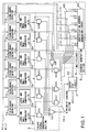
- Fig. 1 is a circuit diagram showing the structure of the address generating circuit of two-dimensional coding table according to a first embodiment of this invention.
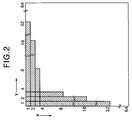
- Fig. 2 is a state diagram showing the distributed condition of coded words of the two-dimensional coding table which is subjected to the treatment according to the embodiment of Fig. 1.
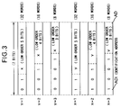
- Fig. 3 is a chart showing the data format of the outputted address signals of the embodiment of Fig. 1.
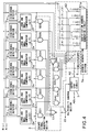
- Fig. 4 is a circuit diagram showing the structure of the address generating circuit of two-dimensional coding table according to a second embodiment of this invention.
- Fig. 5 is a state diagram showing the distributed condition of coded words of the two-dimensional coding table which is subjected to the treatment according to the embodiment of Fig. 4.
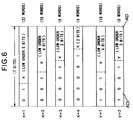
- Fig. 6 is a chart showing the data format of the outputted address signals of the embodiment of Fig. 4.
- Fig. 1 is a circuit diagram showing the structure of the address generating circuit of two-dimensional coding table according to a first embodiment of this invention.
- Fig. 2 is a state diagram showing the distributed condition of coded words of the two-dimensional coding table which is subjected to the address generating circuit of Fig. 1.
- the address generating circuit of this embodiment is intended for a two-dimensional coding table which determines the value of event A as x and the value of event B as y (x and y are positive integral numbers) between two events A and B, corresponds respective coded word to a combination of x and y consisting of x which satisfies x + log2y ⁇ P with respect to each integral number of from 1 through S (S is the maximum value among integral numbers meeting S + log2S ⁇ P , and P is a positive integral number) and y which satisfies y + log2x ⁇ P with respect to each integral number of from 1 through S, and stores the applicable coded word in an address which is disposed to correspond to each combination of x and y.
- the value x of event A determines the number of bits in an effective range of the value y of event B
- the value y of event B determines the number of bits in an effective range of the value x of event A.
- the coded words are distributed in the range of y which is represented by 4 bits
- the coded words are distributed in the range of y which is represented by 3 bits.
- This embodiment shown in Fig. 1 comprises a plurality of coincidence detectors 1a to 1f which input values x and y of events A and B and detect whether the input values coincide with integral numbers 1 to 3, large and small comparators 2a to 2c which detect whether the inputted y satisfies x + log2y ⁇ 6 for each integral number of from 1 to 3 of x, large and small comparators 2d to 2f which detect whether the inputted x satisfies y + log2x ⁇ 6 for each integral number of from 1 to 3 of y, an escape signal generation section 3 which outputs an escape signal according to the output of the coincidence detectors 1a to 1f and the large and small comparators 2a to 2f, an address generation section 5 which generates and outputs an address signal from values x and y and an identification address ADi for identifying that x and y are which of integral numbers of 1 to 3, a priority control section 4 which inputs the output from the coincidence detectors 1a to 1f, determines a signal which is outputted with
- the coincidence detectors 1a to 1f consist of the coincidence detectors 1a to 1c for inputting x and the coincidence detectors 1d to 1f for inputting y. And, they detect whether the inputted x and y coincide with integral numbers 1 to 3, the coincidence detectors 1a and 1d output a coincidence detection signal which becomes an active level when y is 1, the coincidence detectors 1b and 1e output a coincidence detection signal which becomes an active level when y is 2, and the coincidence detectors 1c and 1f output a coincidence detection signal which becomes an active level when y is 3.
- the escape signal generation section 3 has AND type logic gates G31 to G36 and NOR type logic gate G37.
- the logic gates G31 to G36 input one detection signal from the coincidence detectors 1a to 1f and a compared result signal from the large and small comparators 2a to 2f, and the logic gate G37 inputs an output signal from the logic gates G31 to G36. And, when there is no combination at an active level among combinations of coincidence detection signals and compared result signals corresponding thereto, escape signal ES at an active level is outputted.
- the address generation section 5 has an identification address generating circuit 51 which generates an identification address ADi for identifying that x and y are which of integral numbers of 1 to 3, couples each identification address ADi of y with a certain bit at lower order of the inputted x to output respectively as an address signal AD of 7 bits.
- Fig. 3 shows the data format of the address AD thus generated.
- the priority control section 4 has NOR type logic gate G41 and AND type logic gates G42 to G44.
- the logic gate G41 inputs a coincidence detection signal from the coincidence detectors 1d to 1f
- the logic gates G42 to G44 input the coincidence detection signals from the coincidence detectors 1a to 1c and the output from the logic gate G41.
- both the coincidence detection signals on x side and the coincidence detection signals on y side include signals at an active level
- the coincidence detection signal on y side is masked, and the coincidence detection signal on x side only is outputted with precedence.
- both the coincidence detection signal on x side and the coincidence detection signal on y side are outputted as they are.
- a possibility that one address signal AD cannot be surely selected can be avoided.
- the multiplexer 6 selects and outputs the address signal AD containing an identification address ADi corresponding to the applicable x or y among the address signal AD which is outputted from the address generation section 5, according to the coincidence detection signal at an active level of the coincidence detectors 1a to 1f.
- the circuit scale can be made small. And, the memory capacity of the memory for the two-dimensional coding table is also sufficient in the numbers for addresses corresponding to P+1 bit. Further, since processing is directly made through hardware, high-speed processing in real time is possible.
- Fig. 4 is a circuit diagram showing the structure of the address generating circuit of two-dimensional coding table according to a second embodiment of this invention.
- Fig. 5 is a state diagram showing the distributed condition of coded words of the two-dimensional coding table which is subjected to the address generating circuit of Fig. 4.
- the address generating circuit of this embodiment is intended for a two-dimensional coding table which determines the value of event A as x and the value of event B as y (x and y are positive integral numbers) between two events A and B, corresponds respective coded word to a combination of x and y consisting of x which satisfies x + log2y ⁇ P with respect to each integral number of from 1 through S (S is the maximum value among integral numbers satisfying 2 (P-S) - 1 ⁇ Q - log2S , and P and Q are positive integral numbers) and y which satisfies y + log2x ⁇ Q with respect to each integral number of from 1 through R (R is the maximum value among integral numbers satisfying 2 (Q-R) - 1 ⁇ P - log2R ), and stores the applicable coded word in an address which is disposed to correspond to each combination of x and y.
- This embodiment shown in Fig. 1 comprises a plurality of coincidence detectors 1a to 1e and 1g which input values x and y of events A and B and detect whether the inputted values x coincide with integral numbers 1 to 4 and the inputted values y coincide with integral numbers 1 to 2, large and small comparators 2a to 2c and 2g which detect whether the inputted y satisfies x + log2y ⁇ 6 for each integral number of from 1 to 4 of x, large and small comparators 2e to 2f which detect whether the inputted x satisfies y + log2x ⁇ 6 for each integral number of from 1 to 2 of y, an escape signal generation section 3 which outputs an escape signal according to the output of the coincidence detectors 1a to 1e and 1g and the large and small comparators 2a to 2c and 2e to 2g, an address generation section 5 which generates and outputs an address signal from values x and y and an identification address ADi for identifying that x and y are which of integral numbers of 1 to 3,
- This embodiment is slightly different from the first embodiment in the circuit structure, the contents of the address signal AD and others. But such differences are not essential, and the basic operation and effects are same with the first embodiment. More specifically, the coincidence detectors, large and small comparators and others are sufficient in the number corresponding to the number added with the maximum number of integral number S satisfying 2 (P-S) - 1 ⁇ Q - log2S and the maximum number of integral number R satisfying 2 (Q-R) - 1 ⁇ P - log2R , so that the circuit scale can be made small. And, the memory capacity of the memory for the two-dimensional coding table is also sufficient in the numbers for addresses corresponding to a larger number of P or Q+1 bits. Further, since processing is directly made through hardware, high-speed processing in real time is possible.
- this invention is provided with needed and sufficient number of coincidence detectors and comparators derived according to the contributed state of codes and a means for generating an address signal with needed and sufficient address numbers similarly derived, and has the structure to select the address signal according to the output signal of the above coincidence detectors and to generate the escape signal according to the output signal of the above coincidence detectors and comparators, so that it has an effect that the memory capacity of the two-dimensional coding table and the circuit scale can be made small.
- This invention also has an effect of making a high-speed recessing in real time since the processing can be directly made through hardware.
Landscapes
- Engineering & Computer Science (AREA)
- Theoretical Computer Science (AREA)
- Compression, Expansion, Code Conversion, And Decoders (AREA)
Applications Claiming Priority (2)
| Application Number | Priority Date | Filing Date | Title |
|---|---|---|---|
| JP16013/93 | 1993-02-03 | ||
| JP1601393 | 1993-02-03 |
Publications (2)
| Publication Number | Publication Date |
|---|---|
| EP0609835A1 true EP0609835A1 (fr) | 1994-08-10 |
| EP0609835B1 EP0609835B1 (fr) | 1998-09-23 |
Family
ID=11904696
Family Applications (1)
| Application Number | Title | Priority Date | Filing Date |
|---|---|---|---|
| EP94101471A Expired - Lifetime EP0609835B1 (fr) | 1993-02-03 | 1994-02-01 | Circuit de génération d'adresse pour une table de codage à deux dimensions pour un code de Huffman |
Country Status (3)
| Country | Link |
|---|---|
| US (1) | US5553257A (fr) |
| EP (1) | EP0609835B1 (fr) |
| DE (1) | DE69413428T2 (fr) |
Cited By (1)
| Publication number | Priority date | Publication date | Assignee | Title |
|---|---|---|---|---|
| EP0644660B1 (fr) * | 1993-09-14 | 2001-12-12 | Matsushita Electric Industrial Co., Ltd. | Encodeur de codes à longueur variable |
Citations (1)
| Publication number | Priority date | Publication date | Assignee | Title |
|---|---|---|---|---|
| EP0577102A2 (fr) * | 1992-07-02 | 1994-01-05 | Nec Corporation | Circuit de formation d'adresse pour traitement d'images et méthode pour générer les adresses |
Family Cites Families (3)
| Publication number | Priority date | Publication date | Assignee | Title |
|---|---|---|---|---|
| US4545032A (en) * | 1982-03-08 | 1985-10-01 | Iodata, Inc. | Method and apparatus for character code compression and expansion |
| EP0469716B1 (fr) * | 1990-07-03 | 1997-04-23 | Canon Kabushiki Kaisha | Appareil à traitement pour images |
| JPH0486930A (ja) * | 1990-07-31 | 1992-03-19 | Canon Inc | アドレス発生回路 |
-
1994
- 1994-02-01 DE DE69413428T patent/DE69413428T2/de not_active Expired - Fee Related
- 1994-02-01 US US08/189,680 patent/US5553257A/en not_active Expired - Fee Related
- 1994-02-01 EP EP94101471A patent/EP0609835B1/fr not_active Expired - Lifetime
Patent Citations (1)
| Publication number | Priority date | Publication date | Assignee | Title |
|---|---|---|---|---|
| EP0577102A2 (fr) * | 1992-07-02 | 1994-01-05 | Nec Corporation | Circuit de formation d'adresse pour traitement d'images et méthode pour générer les adresses |
Non-Patent Citations (1)
| Title |
|---|
| A. PURI ET AL.: "Adaptative frame/field motion compensated video coding", SIGNAL PROCESSING. IMAGE COMMUNICATION, vol. 5, no. 1/2, February 1993 (1993-02-01), AMSTERDAM NL, pages 39 - 58 * |
Cited By (1)
| Publication number | Priority date | Publication date | Assignee | Title |
|---|---|---|---|---|
| EP0644660B1 (fr) * | 1993-09-14 | 2001-12-12 | Matsushita Electric Industrial Co., Ltd. | Encodeur de codes à longueur variable |
Also Published As
| Publication number | Publication date |
|---|---|
| EP0609835B1 (fr) | 1998-09-23 |
| US5553257A (en) | 1996-09-03 |
| DE69413428T2 (de) | 1999-05-06 |
| DE69413428D1 (de) | 1998-10-29 |
Similar Documents
| Publication | Publication Date | Title |
|---|---|---|
| EP0193185B1 (fr) | Quantificateur de vecteurs de codage interframe adaptable | |
| JP3017380B2 (ja) | データ圧縮方法及び装置並びにデータ伸長方法及び装置 | |
| EP0444717B1 (fr) | Quantificateur de vecteurs | |
| CA1125907A (fr) | Appareil codeur de signaux d'image | |
| EP0481768B1 (fr) | Appareil de codage | |
| US5463701A (en) | System and method for pattern-matching with error control for image and video compression | |
| EP0745946B1 (fr) | Méthode de codage de données et circuit de décodage de données pour la compression de caractères chinois | |
| EP0412047A1 (fr) | Procédé et système pour codage et décodage arithmétique | |
| US4110795A (en) | Method of graphic data redundancy reduction in an optical facsimile system | |
| US4633325A (en) | Adaptive predictive encoding and/or decoding apparatus | |
| US4646148A (en) | Process of compressing a succession of digital data and device for carrying out the same | |
| EP0300775B1 (fr) | Procédé et dispositif de codage et de décodage d'un signal | |
| US4811112A (en) | Vector DPCM image coding method and apparatus | |
| US6091850A (en) | Method of compressing and decompressing graphic images | |
| KR960036647A (ko) | 스캐닝을 이용한 비트플랜 압축전송장치 | |
| US5404138A (en) | Apparatus for decoding variable length codes | |
| US5832131A (en) | Hashing-based vector quantization | |
| US4893187A (en) | Image processing apparatus | |
| EP0609835A1 (fr) | Circuit de génération d'adresse pour une table de codage à deux dimensions | |
| US4467354A (en) | Video format unit | |
| US5091977A (en) | Image data compression method using a run prediction technique | |
| US5173952A (en) | Image filtering system performing transform coding of image data other than boundary picture elements of adjoining blocks | |
| US5404139A (en) | Serial data decoder | |
| US5521641A (en) | Image data coding apparatus and method | |
| US5055919A (en) | Apparatus for image data transposition and compression/decompression |
Legal Events
| Date | Code | Title | Description |
|---|---|---|---|
| PUAI | Public reference made under article 153(3) epc to a published international application that has entered the european phase |
Free format text: ORIGINAL CODE: 0009012 |
|
| AK | Designated contracting states |
Kind code of ref document: A1 Designated state(s): DE FR GB |
|
| 17P | Request for examination filed |
Effective date: 19940829 |
|
| 17Q | First examination report despatched |
Effective date: 19960722 |
|
| GRAG | Despatch of communication of intention to grant |
Free format text: ORIGINAL CODE: EPIDOS AGRA |
|
| GRAG | Despatch of communication of intention to grant |
Free format text: ORIGINAL CODE: EPIDOS AGRA |
|
| GRAH | Despatch of communication of intention to grant a patent |
Free format text: ORIGINAL CODE: EPIDOS IGRA |
|
| GRAH | Despatch of communication of intention to grant a patent |
Free format text: ORIGINAL CODE: EPIDOS IGRA |
|
| GRAA | (expected) grant |
Free format text: ORIGINAL CODE: 0009210 |
|
| AK | Designated contracting states |
Kind code of ref document: B1 Designated state(s): DE FR GB |
|
| REF | Corresponds to: |
Ref document number: 69413428 Country of ref document: DE Date of ref document: 19981029 |
|
| ET | Fr: translation filed | ||
| PLBE | No opposition filed within time limit |
Free format text: ORIGINAL CODE: 0009261 |
|
| STAA | Information on the status of an ep patent application or granted ep patent |
Free format text: STATUS: NO OPPOSITION FILED WITHIN TIME LIMIT |
|
| 26N | No opposition filed | ||
| REG | Reference to a national code |
Ref country code: GB Ref legal event code: IF02 |
|
| PGFP | Annual fee paid to national office [announced via postgrant information from national office to epo] |
Ref country code: GB Payment date: 20030129 Year of fee payment: 10 |
|
| PGFP | Annual fee paid to national office [announced via postgrant information from national office to epo] |
Ref country code: FR Payment date: 20030210 Year of fee payment: 10 |
|
| PGFP | Annual fee paid to national office [announced via postgrant information from national office to epo] |
Ref country code: DE Payment date: 20030213 Year of fee payment: 10 |
|
| REG | Reference to a national code |
Ref country code: GB Ref legal event code: 732E |
|
| REG | Reference to a national code |
Ref country code: FR Ref legal event code: TP |
|
| PG25 | Lapsed in a contracting state [announced via postgrant information from national office to epo] |
Ref country code: GB Free format text: LAPSE BECAUSE OF NON-PAYMENT OF DUE FEES Effective date: 20040201 |
|
| PG25 | Lapsed in a contracting state [announced via postgrant information from national office to epo] |
Ref country code: DE Free format text: LAPSE BECAUSE OF NON-PAYMENT OF DUE FEES Effective date: 20040901 |
|
| GBPC | Gb: european patent ceased through non-payment of renewal fee |
Effective date: 20040201 |
|
| PG25 | Lapsed in a contracting state [announced via postgrant information from national office to epo] |
Ref country code: FR Free format text: LAPSE BECAUSE OF NON-PAYMENT OF DUE FEES Effective date: 20041029 |
|
| REG | Reference to a national code |
Ref country code: FR Ref legal event code: ST |