EP0610949A2 - Statische Halbleiterspeicheranordnung mit verbesserter Soft-Error Immunität - Google Patents
Statische Halbleiterspeicheranordnung mit verbesserter Soft-Error Immunität Download PDFInfo
- Publication number
- EP0610949A2 EP0610949A2 EP94102155A EP94102155A EP0610949A2 EP 0610949 A2 EP0610949 A2 EP 0610949A2 EP 94102155 A EP94102155 A EP 94102155A EP 94102155 A EP94102155 A EP 94102155A EP 0610949 A2 EP0610949 A2 EP 0610949A2
- Authority
- EP
- European Patent Office
- Prior art keywords
- thin film
- channel
- gate electrode
- transistor
- mos transistor
- Prior art date
- Legal status (The legal status is an assumption and is not a legal conclusion. Google has not performed a legal analysis and makes no representation as to the accuracy of the status listed.)
- Withdrawn
Links
Images


Classifications
-
- H—ELECTRICITY
- H10—SEMICONDUCTOR DEVICES; ELECTRIC SOLID-STATE DEVICES NOT OTHERWISE PROVIDED FOR
- H10B—ELECTRONIC MEMORY DEVICES
- H10B10/00—Static random access memory [SRAM] devices
- H10B10/12—Static random access memory [SRAM] devices comprising a MOSFET load element
- H10B10/125—Static random access memory [SRAM] devices comprising a MOSFET load element the MOSFET being a thin film transistor [TFT]
-
- Y—GENERAL TAGGING OF NEW TECHNOLOGICAL DEVELOPMENTS; GENERAL TAGGING OF CROSS-SECTIONAL TECHNOLOGIES SPANNING OVER SEVERAL SECTIONS OF THE IPC; TECHNICAL SUBJECTS COVERED BY FORMER USPC CROSS-REFERENCE ART COLLECTIONS [XRACs] AND DIGESTS
- Y10—TECHNICAL SUBJECTS COVERED BY FORMER USPC
- Y10S—TECHNICAL SUBJECTS COVERED BY FORMER USPC CROSS-REFERENCE ART COLLECTIONS [XRACs] AND DIGESTS
- Y10S257/00—Active solid-state devices, e.g. transistors, solid-state diodes
- Y10S257/903—FET configuration adapted for use as static memory cell
- Y10S257/904—FET configuration adapted for use as static memory cell with passive components,, e.g. polysilicon resistors
Definitions
- the present invention relates to a static semiconductor memory device, and in particular, to a static semiconductor memory having a plurality of memory cells each of which includes a driving transistor formed of a bulk type MOS transistor and a load formed of a thin film transistor.
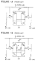
- FIG. 1A there is shown an equivalent circuit of one memory cell in a typical static semiconductor memory device in the prior art.
- the memory cell shown in Figure 1A includes a first inverter circuit composed of a P channel thin film transistor T1 and an N channel MOS transistor T2, and a second inverter circuit composed of a P channel thin film transistor T3 and an N channel MOS transistor T4.
- a flip flop is composed of a cross conjunction of these two inverter circuits, and the flipflop constitutes one memory cell. Data of "1" or "0" can be memorized in memory nodes N1 and N2 of this memory cell.
- N channel MOS transistor T5 and T6 are provided as a transmission gate used to write data to the memory cell and to read data from the memory cell.
- a gate electrode of each of these MOS transistors is connected to a word line W L
- one of source/drain regions of each of these MOS transistors is connected to a corresponding bit line B L
- the other source/drain region is connected to the corresponding memory node N1 or N2 of the memory cell.
- the load transistor (transistor T1, T3 in Figure 1A) of each of the pair of inverters constituting each one flipflop is composed of a P channel thin film transistor, which is in turn located above a bulk type N channel MOS transistor (transistor T2, T4 of Figure 1A) which forms the driving transistor of the inverter.
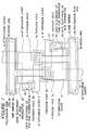
- FIG. 2 there is shown a diagrammatic layout pattern of the above mentioned memory cell circuit in a semiconductor integrated circuit device.
- N+ type impurity regions 1a, 1b and 1c are selectively formed at a surface region of a P-type semiconductor substrate (not shown) made of for example silicon. These N+ type impurity regions 1a, 1b and 1c constitute respective source/drain regions of the transistors T6 and T4 of Figure 1A. In addition, N+ type impurity regions 1d, 1e and 1f are also selectively formed at the surface region of the same P-type semiconductor substrate so as to respective constitute source/drain regions of the transistors T5 and T2.
- Respective gate electrodes 2a and 2b of the transistors T4 and T2 are formed of a first level polysilicon film, and word lines 3a and 3b are also formed of the first level polysilicon film.
- the word lines 3a and 3b also functions as a gate electrode of the transistor T6 and T5, respectively.
- Ground wirings 4a and 4b are formed of a second level polysilicon layer which is formed at a level higher than the first second level polysilicon layer. These ground wirings 4a and 4b are interconnected through through-holes 5a and 5b to the N+ diffusion layers 1c and 1f, respectively.
- Respective gate electrodes 6a and 6b of the P channel thin film transistors are formed of a third level polysilicon film which is formed at a level higher than the second second level polysilicon layer.
- the gate electrode 6a is connected to both of the gate electrode 2b and the N+ type diffusion layer 1b through a through-hole 7a.
- the gate electrode 6b is connected to both of the gate electrode 2a and N+ type diffusion layer 1e through a through-hole 7b.
- Fourth level polysilicon film 8c and 8d which are formed at a level higher than the third second level polysilicon layer, constitute a channel region and source/drain regions of the P channel thin film transistor and also constitute a Vcc wiring.
- the polysilicon film 8c is connected to the gate electrode 6b of the thin film transistor by a through-hole 9a, and similarly, the polysilicon film 8d is connected to the gate electrode 6a of the thin film transistor by a through-hole 9b.
- a through-hole for connecting with a bit line is formed on each of the N+ type diffusion layers 1a and 1d.
- Figure 3A shows a thin film transistor part extracted from Figure 2
- Figure 3B is a cross-sectional view taken along the line A-A in Figure 2.
- a polysilicon film 80 formed of the fourth level polysilicon film is located above the gate electrode 60 formed of the third level polysilicon film through an insulation layer 100 interposed therebetween.
- the polysilicon film 80 is divided into a source region 80a which also functions as the Vcc wiring, a drain region 80b and a channel region 80c.
- the source region 80a is a P type high impurity density region
- the drain region 80b is composed of a P type high impurity region 80b1 and a P type low impurity density region 80b2. These regions are formed by an ion implantation of boron.
- the high impurity density region 80b1 of the drain region is formed apart from the gate electrode 60. This is principally for the purpose of lowering a leak current in an off condition.
- the thin film transistor T1 continues to keep its ON state and the MOS transistor T2 continues to keep its OFF state, and in a short time, the electric potential of the memory node N1 recovers the high level. Accordingly, the soft error immunity is ameliorated in the improved semiconductor memory device mentioned above.
- the injection amount of phosphorus into the gate electrode of the thin film resistor is reduced to a degree of 1 ⁇ 1017 to 1 ⁇ 1019 atoms/cm3.
- a great dispersion of the sheet resistance occurs dependently upon inevitable variations in the manufacturing condition.
- Another object of the present invention is to provide a high reliable static semiconductor memory device has a greater immunity from a soft error caused by an external disturbance such as ⁇ -ray, with no dispersion in characteristics caused dependently upon the manufacturing conditions.
- a static semiconductor memory device including a plurality of memory cells each composed of a first inverter and a second inverter which are cross-connected with each other, said first inverter being composed of a driving transistor formed of a first bulk type N channel MOS transistor and a load transistor formed of a first P channel thin film transistor, and said second inverter being composed of a driving transistor formed of a second bulk type N channel MOS transistor and a load transistor formed of a second P channel thin film transistor, wherein the improvement including a capacitor connected between a gate electrode and a drain of each of the first and second thin film transistors.
- the capacitor may be formed between a gate electrode of of each of the first and second P channel thin film transistors and an extension part which constitutes a drain region of the same P channel thin film transistor and which extends over a channel region of the same P channel thin film transistor.
- the capacitor may be formed between the gate electrode of the first (or second) P channel thin transistor and a gate electrode of the second (or first) bulk type N channel MOS transistor with an insulation film being interposed therebetween.
- a resistor may be connected between the gate electrode of the first (or second ) P channel thin film transistor and the gate electrode of the first (or second ) bulk type N channel MOS transistor.
- This resistor can be formed by making the gate electrode of the thin film transistor by a thin film of a low impurity density semiconductor or a non-doped semiconductor.
- FIG 4 there is shown an equivalent circuit diagram of one memory cell of a number of memory cells included in the first embodiment of the static semiconductor memory device in accordance with the present invention.
- elements similar or corresponding to those shown in Figure 1B are given the same Reference Symbols. Therefore, Reference Symbols T1 and T3 designate a P channel thin film transistor, and Reference Symbols T2, T4, T5 and T6 indicate a bulk type N channel MOS transistor.
- the transistor T1 and T2 are interconnected so as to constitute a first inverter in the form of a so-called CMOS inverter, as shown in Figure 4.
- a source of the P channel transistor T1 is connected to a positive voltage supply voltage Vcc, and a drain of the P channel transistor T1 is connected to a drain of the N-channel transistor T2.
- a source of the N-channel transistor T2 is grounded, and in addition, a gate of the P-channel transistor T1 is connected through a resistor R1 to a gate of the N-channel transistor T2.
- the transistor T3 and T4 are also interconnected so as to constitute a second inverter of the CMOS inverter form. These two inverters are cross-connected with each other in such a manner that an output of each of the inverters is connected to an input of the other inverter. Accordingly, the output of the first inverter is a first memory node N1, and the output of the second inverter is a second memory node N2 complementary to the memory node N1.
- Each of the transistor T5 and T6 constitutes a transfer gate for writing data to the memory cell constructed as mentioned above and for reading data from the memory cell.
- a gate electrode of each of these transistors is connected to a word line W L , and one of a pair of source/drain regions of each of these transistors is connected to a corresponding one of a pair of complementary bit lines B L and B L , and the other source/drain region of each of these transistors is connected to the corresponding memory node N1 or N2.
- a current supplying ability of the transistor T1 greatly increases after the ⁇ -ray hitting, and therefore, the transistor T1 rapidly charges up the memory node N1 so that the electric potential of the node N1 rapidly recovers from -1V to 2V.
- the soft error immunity of the static semiconductor memory device is greatly improved.
- FIG 5 there is shown a diagrammatic layout pattern of the first embodiment of the present invention.
- elements similar or corresponding to those shown in Figure 2 are given the same Reference Numerals.
- N+ type impurity regions 1a, 1b and 1c are selectively formed at a surface region of a P type silicon substrate and are continuous to each other so as to depict an L-shaped pattern having a horizontal arm, a vertical arm and a corner coupling between the horizontal arm and the vertical arm in Figure 5.
- These N+ type impurity regions 1a, 1b and 1c constitute respective source/drain regions of the N channel MOS transistors T6 and T4.
- the source/drain region 1b is in common to both of the N channel MOS transistors T6 and T4.
- N+ type impurity regions 1d, 1e and 1f are also selectively formed at the surface region of the same P type semiconductor substrate so as depict an L-shaped pattern and to constitute respective source/drain regions of the N+ channel MOS transistors T5 and T2.
- the source/drain region 1e is in common to both of the N channel MOS transistors T5 and T2.
- Respective gate electrodes 2a and 2b of the N channel MOS transistors T4 and T2 are formed of a first level polysilicon film to vertically cross the horizontal arm of the corresponding N+ type impurity regions 1c and 1f, respectively.
- Word lines 3a and 3b which are also formed of the first level polysilicon film, horizontally extend at the outside of the N+ type impurity regions 1b, 1c, 1e and 1f and at the outside of the gate electrodes 2a and 2b so as to cross the vertical arm of the corresponding N+ type impurity regions 1a and 1d, respectively. Therefore, the word lines 3a and 3b also constitute the gate electrode of the transistors T6 and T5, respectively.
- Ground wire 4a and 4b are formed of a second level polysilicon film which is located at a level higher than the first second level polysilicon layer. These ground wire 4a and 4b are positioned between the word lines 3a and 3b and to extend substantially over the corresponding N+ type impurity regions 1b and 1c and 1e and 1f, respectively. These ground wire 4a and 4b are interconnected through through-holes 5a and 5b to the N+ diffusion layer 1c and 1f, respectively.
- Respective gate electrodes 6a and 6b of the P channel thin film transistors are formed of a third level polysilicon film which is located at a level higher than the second second level polysilicon layer.
- Each of these gate electrodes 6a and 6b is in an L-shaped pattern having a horizontal portion extending over the corresponding gate electrode 2a or 2b.
- a tip end of a vertical portion of the L-shaped gate electrode 6a is connected to both of the gate electrode 2b and the N+ diffusion layer 1b through a through-hole 7a.
- a tip end of a vertical portion of the gate electrode 6b is connected to both of the gate electrode 2a and the N+ diffusion layer 1e by a through-hole 7b.
- Fourth level polysilicon films 8a and 8b which are formed at a level higher than the third second level polysilicon layer, horizontally extend above and along the, corresponding word lines 3a and 3b, respectively, so as to constitute a Vcc wiring.
- Each of the fourth level polysilicon films 8a and 8b has a vertical portion extending perpendicularly from the horizontal portion to extend along and above the corresponding gate electrode 2a or 2b and to cross the corresponding gate electrode 6a or 6b. Therefore, this vertical portion of the fourth level polysilicon film constitutes a channel region and a pair of source/drain regions of each P channel thin film transistor.
- the polysilicon film 8a is connected to the gate electrode 6b of the thin film transistor through a through-hole 9a, and the polysilicon film 8b is connected to the gate electrode 6a of the thin film transistor though a through-hole 9b.
- a through hole for connecting with the corresponding bit line is formed on each of the N+ type diffusion regions 1a and 1d.
- first, second, third and fourth level polysilicon layers are isolated from one another by an interlayer insulating film that is omitted from the drawing for simplification of the drawing.
- the N channel MOS transistors T6 and T4 are formed by the N+ type impurity regions 1a, 1b and 1c as mentioned above, it can be considered that the thin film transistor T3 is formed by the polysilicon film 8b, and the resistor R1 is formed of a portion of the gate electrode 6a starting from the through hole 7a and terminating at a point crossing the polysilicon film 8a.
- the thin film transistor T1 is formed by the polysilicon film 8a, and the resistor R2 is formed of a portion of the gate electrode 6b starting from the through hole 7b and terminating at a point crossing the polysilicon film 8b.
- the gate electrode of each thin film transistor can be formed of a thin film made of a low impurity density semiconductor or a non-doped semiconductor.
- FIG. 5 The diagrammatic layout pattern shown in Figure 5 is almost the same as that of Figure 2 in the pattern of the semiconductor layers. A difference is only that the polysilicon films 8c and 8d in the prior art example are replaced with the polysilicon films 8a and 8b of this embodiment. Both the polysilicon films 8a, 8b and 8c, 8d have an N type region doped with phosphorus (P) and a P-type region doped with boron (B), but the polysilicon films 8a, 8b and 8c, 8d are different in the pattern of the boron-doped P type region. This point will be explained more in detail with reference to Figure 6.
- P phosphorus
- B P-type region doped with boron
- Figure 6A is a drawing of the thin film transistor part extracted from Figure 5, and Figure 6B is a diagrammatic sectional view taken along the line B-B in Figure 6A.
- a polysilicon film 80 formed of the fourth level polysilicon film is located above the gate electrode 60 formed of the third level polysilicon film with an insulation film 100 being interposed therebetween.
- the polysilicon film 80 is divided to a source region 80a which also constitutes the Vcc wiring, a drain region 80b and a channel region 80c.
- the source region 80a is a P type high impurity density region
- the drain region 80b is composed of a P type high impurity density region 80b1 and a P type low impurity density region 80b2
- the channel region 80c is composed of a region remained as an N type region 80c1 and a P-type low impurity density region 80c2 doped with boron.
- a capacitor is formed between the low impurity density region 80c2 and the gate electrode 60.
- This capacitor corresponds to the capacitor connected between the drain and the gate of each of the thin film transistors T1 and T3 as shown in Figure 4. From another view point, the low impurity density region 80c2 can be deemed to be an extension of the drain region 80b extending over a portion of the gate electrode 60.
- the dose of borons injected for the high impurity density region 80b1 is about 1 ⁇ 1015 to 1 ⁇ 1016/cm2, and the dose of borons injected for the low impurity density regions 80b2 and 80c2 are about 1 ⁇ 1012 to 1 ⁇ 1013 /cm2.
- a more distinguishable effect of the present invention can be obtained by forming the gate electrode of the thin film transistor by a thin film of a low impurity density semiconductor or a non-doped semiconductor as mentioned above, in addition to the addition of the capacitors. Because, the above mentioned bootstrap effect may be enhanced, in addition to respective effects of the capacitors and the resistors.
- Figure 7 is a layout pattern of the second embodiment.
- elements corresponding to those in the first embodiment shown in Figure 5 are given the same Reference Numerals, and explanation thereof will be omitted.
- a point of this embodiment different from the first embodiment is that the configuration of the ground wirings 4a and 4b formed of the second level polysilicon film in the first embodiment is replaced with ground wirings 4c and 4d which are modified to a form retreated from the N+ diffusion region, in comparison with the ground wirings 4a and 4b in the first embodiment.
- each of the ground wirings 4c and 4d extends substantially above and along the corresponding word line 3a or 3b, and has a vertical extension 4c1 or 4d1 extending perpendicularly toward the corresponding through hole 5a or 5b, without overlapping with the corresponding gate electrode 2a or 2b.
- the ground wirings 4a and 4b formed of the second level polysilicon film are interposed between the gate electrode 2a and 2b of the MOS transistors T4 and T2 formed of the first level polysilicon film and the gate electrodes 6a and 6b of the thin film transistors T1 and T3 formed of the third level polysilicon film.
- the gate electrodes 2a and 2b of the MOS transistor T4 and T2 and the gate electrodes 6a and 6b of the thin film transistors T1 and T3 are arranged face to face with interposing no ground wiring therebetween.
- the capacitor is connected between the gate electrode and the drain of each of the P-channel thin film transistors which function as a load of the memory cell, the drop of electric potential at the memory node of the memory cell caused by the irradiation of ⁇ -ray can be recovered immediately. Therefore, it is possible to greatly ameliorate the soft error immunity.
Landscapes
- Semiconductor Memories (AREA)
- Internal Circuitry In Semiconductor Integrated Circuit Devices (AREA)
- Thin Film Transistor (AREA)
Applications Claiming Priority (2)
| Application Number | Priority Date | Filing Date | Title |
|---|---|---|---|
| JP5047238A JP2518133B2 (ja) | 1993-02-12 | 1993-02-12 | スタティック型半導体記憶装置 |
| JP47238/93 | 1993-02-12 |
Publications (2)
| Publication Number | Publication Date |
|---|---|
| EP0610949A2 true EP0610949A2 (de) | 1994-08-17 |
| EP0610949A3 EP0610949A3 (en) | 1995-11-08 |
Family
ID=12769640
Family Applications (1)
| Application Number | Title | Priority Date | Filing Date |
|---|---|---|---|
| EP94102155A Withdrawn EP0610949A3 (en) | 1993-02-12 | 1994-02-11 | Static semiconductor memory device having increased soft error immunity. |
Country Status (3)
| Country | Link |
|---|---|
| US (1) | US5406107A (de) |
| EP (1) | EP0610949A3 (de) |
| JP (1) | JP2518133B2 (de) |
Families Citing this family (17)
| Publication number | Priority date | Publication date | Assignee | Title |
|---|---|---|---|---|
| US5508540A (en) * | 1993-02-19 | 1996-04-16 | Hitachi, Ltd. | Semiconductor integrated circuit device and process of manufacturing the same |
| JPH07235645A (ja) * | 1993-12-29 | 1995-09-05 | Mitsubishi Electric Corp | スタティック型半導体記憶装置およびその製造方法 |
| TW297158B (de) * | 1994-05-27 | 1997-02-01 | Hitachi Ltd | |
| CN1129967C (zh) * | 1995-04-17 | 2003-12-03 | 精工爱普生株式会社 | 半导体装置及其制造方法 |
| GB9520888D0 (en) * | 1995-10-12 | 1995-12-13 | Philips Electronics Nv | Electronic devices comprising thin-film circuitry |
| KR100214843B1 (ko) * | 1996-03-29 | 1999-08-02 | 김주용 | 반도체 소자 및 그의 제조방법 |
| JPH09270469A (ja) * | 1996-03-29 | 1997-10-14 | Sanyo Electric Co Ltd | 半導体メモリ装置 |
| US5982000A (en) * | 1998-04-03 | 1999-11-09 | Ericsson Inc. | Resistive interconnect of transistor cells |
| JP2002176112A (ja) * | 2000-12-08 | 2002-06-21 | Mitsubishi Electric Corp | 半導体記憶装置およびその製造方法 |
| JP2003046085A (ja) * | 2001-08-01 | 2003-02-14 | Seiko Epson Corp | 半導体装置及びその製造方法 |
| JP2003173681A (ja) * | 2001-12-07 | 2003-06-20 | Mitsubishi Electric Corp | 半導体メモリ回路およびラッチ回路 |
| JP2004013920A (ja) | 2002-06-03 | 2004-01-15 | Mitsubishi Electric Corp | 半導体記憶装置 |
| JP2004079843A (ja) * | 2002-08-20 | 2004-03-11 | Renesas Technology Corp | 半導体記憶装置 |
| JP2004207282A (ja) * | 2002-12-20 | 2004-07-22 | Fujitsu Ltd | 不揮発性半導体記憶装置、及び不揮発性半導体記憶装置の製造方法 |
| US8189367B1 (en) * | 2007-02-23 | 2012-05-29 | Bae Systems Information And Electronic Systems Integration Inc. | Single event upset hardened static random access memory cell |
| US9466618B2 (en) * | 2011-05-13 | 2016-10-11 | Semiconductor Energy Laboratory Co., Ltd. | Semiconductor device including two thin film transistors and method of manufacturing the same |
| US10297781B2 (en) * | 2016-06-30 | 2019-05-21 | Lg Display Co., Ltd. | Organic light emitting display device and driving method of the same |
Family Cites Families (8)
| Publication number | Priority date | Publication date | Assignee | Title |
|---|---|---|---|---|
| JPS6038864A (ja) * | 1983-08-11 | 1985-02-28 | Nec Corp | 半導体メモリセル |
| JPH0685431B2 (ja) * | 1985-06-10 | 1994-10-26 | 株式会社日立製作所 | 半導体装置 |
| US5016070A (en) * | 1989-06-30 | 1991-05-14 | Texas Instruments Incorporated | Stacked CMOS sRAM with vertical transistors and cross-coupled capacitors |
| JPH03218667A (ja) * | 1989-11-01 | 1991-09-26 | Hitachi Ltd | 半導体記憶装置 |
| US5350933A (en) * | 1990-02-21 | 1994-09-27 | Sony Corporation | Semiconductor CMOS static RAM with overlapping thin film transistors |
| JP2599495B2 (ja) * | 1990-09-05 | 1997-04-09 | シャープ株式会社 | 半導体装置の製造方法 |
| JP3231345B2 (ja) * | 1991-03-08 | 2001-11-19 | 株式会社日立製作所 | 半導体記憶装置及びその製造方法 |
| JPH04334054A (ja) * | 1991-05-09 | 1992-11-20 | Mitsubishi Electric Corp | 半導体装置、電界効果トランジスタおよびその製造方法 |
-
1993
- 1993-02-12 JP JP5047238A patent/JP2518133B2/ja not_active Expired - Fee Related
-
1994
- 1994-02-11 EP EP94102155A patent/EP0610949A3/en not_active Withdrawn
- 1994-02-14 US US08/195,034 patent/US5406107A/en not_active Expired - Lifetime
Also Published As
| Publication number | Publication date |
|---|---|
| JP2518133B2 (ja) | 1996-07-24 |
| EP0610949A3 (en) | 1995-11-08 |
| JPH06244385A (ja) | 1994-09-02 |
| US5406107A (en) | 1995-04-11 |
Similar Documents
| Publication | Publication Date | Title |
|---|---|---|
| EP0610949A2 (de) | Statische Halbleiterspeicheranordnung mit verbesserter Soft-Error Immunität | |
| US6057188A (en) | Trench capacitor structures | |
| US4849801A (en) | Semiconductor memory device having increased capacitance for the storing nodes of the memory cells | |
| US5072286A (en) | Semiconductor memory device having memory cells including IG FETs in a symmetrical arrangement | |
| US5298782A (en) | Stacked CMOS SRAM cell with polysilicon transistor load | |
| US4797804A (en) | High density, high performance, single event upset immune data storage cell | |
| US6756692B2 (en) | Semiconductor storage device having high soft-error immunity | |
| US5677866A (en) | Semiconductor memory device | |
| US5206533A (en) | Transistor device with resistive coupling | |
| US6271568B1 (en) | Voltage controlled resistance modulation for single event upset immunity | |
| KR100305440B1 (ko) | 반도체집적회로장치 | |
| US5281843A (en) | Thin-film transistor, free from parasitic operation | |
| US5388067A (en) | Semiconductor memory cell | |
| US4725875A (en) | Memory cell with diodes providing radiation hardness | |
| US20080026524A1 (en) | Semiconductor device having a well structure for improving soft error rate immunity and latch-up immunity and a method of making such a device | |
| US4833644A (en) | Memory cell circuit having radiation hardness | |
| JPS6388859A (ja) | ラツチアツプ保護回路付き集積回路 | |
| KR0183485B1 (ko) | 반도체 디바이스 및 그 제조 방법 | |
| JPS6062153A (ja) | 抵抗性ゲ−ト型電界効果トランジスタ論理回路 | |
| US6538338B2 (en) | Static RAM semiconductor memory device having reduced memory | |
| KR960010072B1 (ko) | 반도체 메모리장치 | |
| EP0459380B1 (de) | Statische Halbleiterspeicheranordnung | |
| EP0708449A2 (de) | Sehr schnelle und sehr dichte SRAM-Speicherzelle | |
| US6724676B1 (en) | Soft error improvement for latches | |
| US4903094A (en) | Memory cell structure having radiation hardness |
Legal Events
| Date | Code | Title | Description |
|---|---|---|---|
| PUAI | Public reference made under article 153(3) epc to a published international application that has entered the european phase |
Free format text: ORIGINAL CODE: 0009012 |
|
| AK | Designated contracting states |
Kind code of ref document: A2 Designated state(s): DE FR GB |
|
| PUAL | Search report despatched |
Free format text: ORIGINAL CODE: 0009013 |
|
| AK | Designated contracting states |
Kind code of ref document: A3 Designated state(s): DE FR GB |
|
| 17P | Request for examination filed |
Effective date: 19951017 |
|
| 17Q | First examination report despatched |
Effective date: 19970401 |
|
| STAA | Information on the status of an ep patent application or granted ep patent |
Free format text: STATUS: THE APPLICATION HAS BEEN WITHDRAWN |
|
| 18W | Application withdrawn |
Withdrawal date: 19970929 |