EP0611058A2 - Oscillateur réglé en courant - Google Patents
Oscillateur réglé en courant Download PDFInfo
- Publication number
- EP0611058A2 EP0611058A2 EP94300489A EP94300489A EP0611058A2 EP 0611058 A2 EP0611058 A2 EP 0611058A2 EP 94300489 A EP94300489 A EP 94300489A EP 94300489 A EP94300489 A EP 94300489A EP 0611058 A2 EP0611058 A2 EP 0611058A2
- Authority
- EP
- European Patent Office
- Prior art keywords
- transistor
- coupled
- switching
- output
- current
- Prior art date
- Legal status (The legal status is an assumption and is not a legal conclusion. Google has not performed a legal analysis and makes no representation as to the accuracy of the status listed.)
- Withdrawn
Links
- 230000010355 oscillation Effects 0.000 claims abstract description 35
- 230000010354 integration Effects 0.000 claims abstract description 3
- 239000003990 capacitor Substances 0.000 claims description 15
- 230000008878 coupling Effects 0.000 claims description 2
- 238000010168 coupling process Methods 0.000 claims description 2
- 238000005859 coupling reaction Methods 0.000 claims description 2
- 230000014509 gene expression Effects 0.000 description 9
- 230000000630 rising effect Effects 0.000 description 3
- 238000006880 cross-coupling reaction Methods 0.000 description 2
- 230000000694 effects Effects 0.000 description 2
- 238000010586 diagram Methods 0.000 description 1
- 238000007599 discharging Methods 0.000 description 1
- 238000009738 saturating Methods 0.000 description 1
- 239000000758 substrate Substances 0.000 description 1
Images


Classifications
-
- H—ELECTRICITY
- H03—ELECTRONIC CIRCUITRY
- H03K—PULSE TECHNIQUE
- H03K3/00—Circuits for generating electric pulses; Monostable, bistable or multistable circuits
- H03K3/02—Generators characterised by the type of circuit or by the means used for producing pulses
- H03K3/26—Generators characterised by the type of circuit or by the means used for producing pulses by the use, as active elements, of bipolar transistors with internal or external positive feedback
- H03K3/28—Generators characterised by the type of circuit or by the means used for producing pulses by the use, as active elements, of bipolar transistors with internal or external positive feedback using means other than a transformer for feedback
- H03K3/281—Generators characterised by the type of circuit or by the means used for producing pulses by the use, as active elements, of bipolar transistors with internal or external positive feedback using means other than a transformer for feedback using at least two transistors so coupled that the input of one is derived from the output of another, e.g. multivibrator
- H03K3/282—Generators characterised by the type of circuit or by the means used for producing pulses by the use, as active elements, of bipolar transistors with internal or external positive feedback using means other than a transformer for feedback using at least two transistors so coupled that the input of one is derived from the output of another, e.g. multivibrator astable
- H03K3/2821—Emitters connected to one another by using a capacitor
Definitions
- This invention relates to a current-controlled oscillator topology. More particularly this invention provides a current-controlled oscillator (CCO) topology which is suited for application in a monolithic voltage-controlled oscillator (VCO).
- CO current-controlled oscillator
- a current-controlled oscillator is one of the functional blocks comprising a voltage controlled oscillator.
- current-controlled oscillators can be based on emitter-coupled multivibrators.
- the emitter-coupled multivibrator oscillates at a frequency which is proportional to I/V BE , where V BE is the drop across a clamping diode.
- the frequency of the multivibrator is varied by adjusting I, and is temperature compensated by making current I a function of V BE /R x , where R x is a low temperature coefficient external resister.
- the maximum operation frequency is limited by switching losses and by the collector-substrate capacitance of the coupled transistors combined with the peak-to-peak voltage swing across the base-emitter junctions. Moreover, at high operating frequencies these effects worsen the temperature stability of the emitter-coupled multivibrator. Lastly, the minimum supply voltage for an emitter-coupled multivibrator is determined by the minimum voltage across the current sources which is given by V CC - 3 V BE .
- the present invention addresses these limitations of known emitter-coupled multivibrators by providing a topology for a current-controlled oscillator which has a higher maximum operating frequency, a lower temperature coefficient, and a lower operating supply voltage.
- the present invention provides a current-controlled oscillator circuit which is suitable for monolithic integration, the current controlled oscillator circuit comprising: (a) switching means operating to produce an output signal having an adjustable oscillation frequency; (b) an output port coupled to said switching means for outputting said output signal; (c) frequency control means coupled to said switching means for setting the oscillation frequency of said output signal; and (d) switching control means coupled to said frequency control means and to said switching means, said switching control means including differential control means for controlling said switching means.
- the present invention provides a current-controlled oscillator suitable for use in a phase-locked loop system having a phase detector and a loop filter, said current-controlled oscillator comprising: (a) a monolithically integrated circuit comprising: (i) switching means operating to produce an output signal having an adjustable oscillation frequency; (ii) an output port coupled to said switching means for outputting said output signal to the phase detector stage of the phase-locked loop; (iii) frequency control means coupled to said switching means for setting the oscillation frequency of said output signal, said frequency control means including a control input port coupled to the loop filter for receiving a voltage control signal, said frequency control means also including temperature compensation means; and (iv) switching control means coupled to said frequency control means and to said switching means, said switching control means including differential control means for controlling said switching means; (b) an external resistor coupled to said frequency control means, said external resistor having a low temperature coefficient.
- FIG. 1 shows an emitter-coupled multivibrator 20 (also known as current controlled oscillator abbreviated CCO) according to the present invention.
- the emitter-coupled multivibrator 20 comprises an emitter-coupled switching stage 22, a switching control stage 24, a current control network 26, and an output stage 28.
- the emitter-coupled switching stage 22 comprises a pair of transistors Q1 and Q2 which are matched.
- the emitters of the transistors Q1,Q2 are coupled through a timing capacitor C T .
- the emitter of transistor Q1 is also connected to a first current source 30 and the emitter of transistor Q2 is connected to a second current source 32.
- the current sources 30,32 are also matched, with each sinking a current I1 which biases the respective transistor Q1 or Q2.
- the two current sources 30,32 and a third current source 34 comprise the current control network 26.
- the collectors of the transistors Q1,Q2 are coupled to a positive supply voltage rail V CC through respective resistors R1 and R2 which are matched resistors.
- the transistors Q1 and Q2 are cross-coupled through the switching control stage 24 as will be explained below.
- the switching control stage 24 comprises a pair of transistors Q3 and Q4.
- the emitters of transistors Q3 and Q4 are directly coupled to form a differential amplifier 25.
- the emitters of transistors Q3 and Q4 are also connected to the third current source 34.
- the third current source 34 sinks a current I2 which is the sum of the emitter currents flowing in transistors Q3 and Q4.
- the collectors of transistors Q3 and Q4 are connected to the positive supply rail V CC through respective load resistors R3 and R4 which are matched resistors.
- transistors Q1 and Q2 in the emitter-coupled switching stage 22 are cross-coupled. Cross-coupling assures that either transistor Q1 or transistor Q2 (but not both) is on at any one time.
- Transistors Q1 and Q2 are cross-coupled through transistors Q3 and Q4 which form the differential amplifier 25 in the switching control stage 24.
- the base of transistor Q1 is connected to the collector of transistor Q3 and the collector of transistor Q1 is connected to the base of transistor Q3.
- the base of transistor Q2 is connected to the collector of transistor Q4 and the collector of transistor Q2 is connected to the base of transistor Q4.
- the output stage 28 of the emitter-coupled multivibrator 20 comprises a pair of transistors Q5 and Q6.
- the base of transistor Q5 is connected to the base of transistor Q2 and the collector of transistor Q4.
- the emitter of transistor Q5 is connected to a fourth current source 36, which sinks a current I3.
- the emitter of transistor Q5 provides a voltage output signal V O1 on output line 38.
- Transistor Q5 functions as a unity gain buffer. As a unity gain buffer, the emitter of transistor Q5 follows the signal (i.e. collector output of transistor Q4) which is applied to the base of transistor Q5.
- the voltage gain of transistor Q5 is unity, but the current gain is high thereby providing good drive capability for the output stage 28.
- the base of the other transistor Q6 is connected to the collector of transistor Q3 and the emitter of transistor Q6 is connected to a fifth current source 37.
- the current source 37 also sinks a current I3.
- Transistor Q6 is also configured as an emitter follower or unity gain buffer. Transistor Q6 produces a voltage signal V O2 on output line 39 which is connected to the emitter of transistor Q6. In this way, the two output lines 38,39 provide a buffered output signal V O , i.e. V O1 - V O2 , as will be discussed in more detail below.
- the operation of the emitter-coupled multivibrator 20 can be briefly explained as follows.
- the cross-coupling of transistors Q1 and Q2 through the differential amplifier 25 assures that either transistor Q1 or transistor Q2 (but not both) is on at any one time. In this manner, the timing capacitor C T is alternately charged with equal but opposite currents, first through transistor Q1 and then through transistor Q2, during alternate half-cycles of operation of the switching stage 22.
- transistor Q1 When transistor Q2 switches on, transistor Q1 turns off, and the voltage stored across the timing capacitor C T is given by the expression R3xI2.
- transistor Q2 When transistor Q2 switches on, the base of transistor Q4 is pulled down; and when transistor Q1 turns off, the base of transistor Q3 is pulled up to the positive supply rail V CC . This causes transistor Q3 to turn on and transistor Q4 to turn off and the collector current of transistor Q3 will be current I2.
- transistor Q4 When transistor Q4 turns off, the base of transistor Q2 is pulled up to the positive supply rail V CC by resistor R4.
- transistor Q3 When transistor Q3 turns on, the base of transistor Q1 is pulled down by R3xI2. Now the timing capacitor C T will have to be discharged by 2xR3xI2 before transistor Q1 will conduct current.
- transistor Q1 Since transistor Q1 is cut-off, all of the current I1 from the current source 30 flows through the capacitor C T discharging the voltage level at the emitter of transistor Q1.
- the current I1 flowing through the capacitor C T plus the current I1 from the current source 32, flow through the emitter of transistor Q2 such that (neglecting base current) 2xI1 flows in the collector of transistor Q2.
- the voltage level at the emitter of transistor Q1 drops by 2xR3xI2 then the base-emitter junction of transistor Q1 will be forward biased and transistor Q1 will turn on.
- resistor R3 pulls the base of transistor Q1 to the positive supply rail V CC .
- transistor Q4 switches on and pulls down the base of transistor Q2 by a voltage value which is equal to R4xI2 volts. This causes transistor Q2 to turn off (i.e. cut-off), and the timing capacitor C T must be discharged by a voltage 2xR4xI2 before transistor Q2 will conduct current i.e. turn on.
- the timing capacitor C T produces a voltage signal V CT (i.e. V E (Q1)-V E (Q2) which is a triangular waveform.
- V CT voltage signal
- V E Q1-V E (Q2)
- the voltage output signal V O (which is derived from the voltage signal V CT ) comprises the two half-cycle voltage signal waveforms V O1 and V O2 which are produced at the emitters of transistors Q5 and Q6 respectively.
- the total peak-to-peak voltage swing of the waveforms V O1 and V O2 is 2xI2xR3 volts. This follows because the cut-off transistor (i.e. Q1 or Q2) in the switching stage 22 will turn on when there is a voltage drop of 2xI2xR3 at the respective emitter.
- the voltage signal V O has an oscillation frequency f O .
- the oscillation frequency f O is governed by the resistors R3 and R4 and the timing capacitor C T and the current sources 30,32,34.
- the current sources 30,32 are controlled by a voltage control input V CON as will be discussed in detail below.
- the current source 34 can be controlled by V CON and current sources 30,32 would not be controlled but left constant.
- transistors Q1 and Q2 in the switching stage 22, and transistors Q3 and Q4, in the switching control stage 24, are operated in the active region, i.e. non-saturation region. This can be achieved by having the voltage swing across the load resistors R3 and R4 in the switching control stage 24 ⁇ 400 mV, and the voltage across the resistors R1 and R2 in the switching stage 22 ⁇ 400 mV.
- the rate of discharge of the timing capacitor C T determines the rate at which the transistors Q1 and Q2 switch states, i.e. cut-off to on and vice versa. Since the rate of discharge of the capacitor C T is equal to I1 /C T , adjusting the magnitude of the current I1 sunk by the first and second current sources 30,32 will control the oscillation frequency f O of the emitter-coupled multivibrator 20.
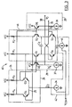
- FIG. 3 shows an emitter-coupled multivibrator 40 according to a second embodiment of the present invention.
- the emitter-coupled multivibrator 40 has the same structure, i.e. the emitter-coupled switching stage 22, the switching control stage 24, and the output stage 28, as the emitter-coupled multivibrator 20 shown in Figure 1 and corresponding reference numerals indicate elements corresponding to those of Figure 1.
- the current control stage indicated by reference 42 is modified as shown in Figure 3.
- the emitter-coupled switching stage as indicated by reference 44 has also been modified to include two additional transistors Q7 and Q8. The function of the two transistors Q7 and Q8 is to reduce switching losses in the switching stage 44 thereby increasing the maximum oscillation frequency f O .
- the collector of transistor Q7 is connected to the emitter of transistor Q2 and the base of transistor Q7 is connected to the emitter of transistor Q6.
- the collector of transistor Q8 is connected to the emitter of transistor Q1 and the base of transistor Q8 is connected to the emitter of transistor Q5.
- the emitters of transistors Q7 and Q8 are connected together and coupled to a current source 46.
- the current source 46 replaces the two current sources 30,32 ( Figure 1) and sinks a current I which is twice the magnitude of current I1.
- the only coupling between the rising edge of the voltage signal V E (Q1) at the emitter of transistor Q1 and the emitter of transistor Q2 was through the timing capacitor C T .
- the base of transistor Q8 is rising at the same time as the emitter of transistor Q2 (through the emitter-follower action of transistor Q5), and the base-collector capacitance of transistor Q8 couples the rising edge of the base transistor Q8 to the emitter of transistor Q1. Since transistors Q2,Q6 and Q7 are a mirror image of transistors Q2,Q5 and Q8, they also function as described above.
- FIG. 4 shows another aspect of the emitter-coupled multivibrator according to the second embodiment of the present invention.
- the emitter-coupled multivibrator shown in Figure 4 is denoted by reference 48.
- the multivibrator 48 shown in Figure 4 is identical to the multivibrator 40 shown in Figure 3 except the configuration of the output transistors Q5 and Q6 have been changed and corresponding reference numerals indicate elements corresponding to those of Figures 1 and 3.
- the base (i.e. input) of transistor Q5 is now connected to the base of transistor Q4 instead of the collector (i.e. output) of transistor Q4.
- the base of the other output transistor Q6 is connected to the base of transistor Q3.
- transistors Q3 and Q4 are turned on when their respective bases are pulled up to the positive supply rail V CC .
- the respective output transistor Q5 or Q6 will also be pulled up when the base of the corresponding transistor Q4 or Q3 is pulled up to the supply rail V CC .
- transistor Q7 or Q8 will be turned on earlier than in the circuit topology for multivibrator 40 shown in Figure 3.
- the emitter-coupled multivibrator 48 shown in Figure 4 will have a higher maximum oscillation frequency f O because the switching of transistors Q7 and Q8 occurs earlier.
- the range of the oscillation frequency f O can be controlled by varying the magnitude of the current I1 (or I). However, increasing the current I1 can put transistors Q1 and Q2 in saturation, i.e. if 2 x I1 x R1 (or R2) ⁇ 0.4 volts .
- the emitter-coupled multivibrator 40 or 48 can include a pair of Schottky diodes Z1 and Z2 (shown in broken outline in Figure 4).
- the Schottky diode Z1 is connected across resistor R1 and the Schottky diode Z2 is connected across R2 to form a simple Schottky clamp.
- the forward voltage of the Schottky diodes Z1 or Z2 should be in the range 300 to 500 mV.
- the circuit topology for the emitter-coupled multivibrator 40 shown in Figure 3 is used when dynamic range is important.
- the current I can be adjusted to vary the oscillation frequency f O without varying the voltage swing of the output voltage signal V O at the emitters of transistors Q5 and Q6.
- the Schottky diodes Z1 and Z2 can be used to prevent transistors Q1 and Q2 from entering saturation as discussed above.
- the circuit topology for the emitter-coupled multivibrator 48 shown in Figure 4 is used when a very high oscillation frequency f O is required.
- the current I2 is adjusted to vary the oscillation frequency f O without varying the peak-to-peak voltage swing of the voltage output signal V O at the emitters of transistors Q5 and Q6.
- Figure 5 shows a circuit topology for a current control network 42 which is suitable for both embodiments of the emitter-coupled multivibrator 40,48 according to the present invention.
- the current control network 42 shown in Figure 5 provides a circuit topology which has a low temperature coefficient, i.e. which is independent of temperature variations on the PN junctions of the transistors Q1 to Q8.
- the current control network 42 comprises current source 34, current source 46, a voltage source 50, a reference resistor R REF and an external resistor R EXT .
- the current source 46 comprises a transistor Q9.
- the collector of transistor Q9 is connected to the emitters of transistors Q7 and Q8 shown in Figures 3 and 4.
- the emitter of transistor Q9 is connected to the external resistor R EXT and a resistor R C .
- Resistor R C is connected to the input which receives the control voltage V CON .
- the other current source 34 in the frequency control network 42 also comprises a transistor Q10.
- the collector of transistor Q10 is connected to the emitters of transistors Q3 and Q4, i.e. the differential amplifier 25, shown in both Figures 3 and 4.
- the base of transistor Q10 is connected to the voltage reference source 50 which produces an output voltage level of V REF + 2V BE volts, where V BE is the forward voltage drop across the base-emitter junction of the transistors.
- the emitter of transistor Q10 is coupled to a diode-connected transistor Q11.
- the emitter of diode-connected transistor Q11 is connected to the reference resistor R REF .
- the voltage level at the emitter of diode-connected transistor Q11 is V REF volts and the voltage level at the emitter of transistor Q9 is also V REF volts.
- the current I which is sunk by transistor Q9 is given by the following expression: and the current I2 which transistor Q10 sinks is determined according to the following expression:
- the currents I and I2 are independent of both the supply voltage V CC and the base-emitter voltage drop V BE which is very susceptible to temperature variation.
- the voltage reference source 50 can have any temperature coefficient without affecting the oscillation frequency f O as can be seen from expression (4).
- the voltage reference source 50 should have a zero temperature coefficient so that for any control voltage V CON , the temperature coefficient for the current I remains unchanged.
- One skilled in the art can modify current control network 42 for operation with the emitter-coupled multivibrator shown in Figure 1.
- the oscillation frequency f O of the output voltage signal V O is varied by adjusting current sources 30,32 (i.e. current I1) or current source 34 (i.e. current I2).
- the oscillation frequency f O is adjusted by setting the current source 34 (i.e. current I2) or the current source 46 (i.e. current I). It will be appreciated by those skilled in the art that adjusting current source 34 (i.e. current I2) will vary the voltage swing at the output stage 28.
- the frequency of oscillation is inversely proportional to the voltage drop V BE which varies at a rate of ⁇ -2 mV/°C T .
- This temperature variance results in a positive temperature coefficient for the oscillation frequency f O .
- a feature of the present invention is that the emitter-coupled multivibrators 20,40,48 are temperature compensated by making the oscillation frequency f O a function of the voltage reference source 50, the reference resistor R REF , and the external resistor R EXT .
- the oscillation frequency f O can be determined as follows.
- Each half-cycle of oscillation, i.e. for voltage signals V E (Q2) and V E (Q1), is given by the following expression: where the peak-to-peak voltage swing, i.e. dv , across the timing capacitor C T is 2xI2xR3 as was discussed above.
- the period of the half-cycle voltage signal V O1 or V 02 is: to determine the period of oscillation, i.e. f O , of the voltage output signal V O , the above expression (2) is merely multiplied by two.
- the oscillation frequency f O is simply the inverse of the period of oscillation T and can be expressed as follows: by making the currents I1 and I2 functions of the voltage reference source 50, the on-chip reference resistor R REF , and the external resistor R EXT , the dependence on a bi-polar junction voltage (i.e. V BE ) which is susceptible to temperature variance is eliminated.
- the reference resistor R REF can be matched to resistor R3 since they are both on-chip resistors, and the external resistor R EXT is selected to have a very low temperature coefficient thereby also not affecting the stability of the oscillation frequency f O .
- the emitter-coupled multivibrators 20,40,48 according to the present invention also provide a higher maximum oscillation frequency f O over the prior art because the peak-to-peak voltage swings of the output voltage signal V O (i.e. ⁇ 400mV) are lower, and therefore switching losses are reduced by the circuit topology of the present and by lower values of resistors R1 and R2 (see below) than for the equivalent resistors in the known emitter-coupled multivibrators (not shown).
- the emitter-coupled multi-vibrators 20,40,48 can operate at lower supply voltages, i.e. V CC , than required for the prior art devices.
- the minimum supply voltage for the first embodiment of the emitter-coupled multivibrator 20 shown in Figure 1 is determined by the minimum voltage across the current sources 30,32,34. It is within the capability of one skilled in the art to calculate that the minimum voltage across the current sources 30,32,34 is V CC -0.4-V BE volts. This is 2V BE -0.4 volts less than the supply voltage required for known devices.
- the minimum voltage across the current source 46 is V CC -0.4-2V BE volts, which presents a V BE -0.4 volt improvement over the prior art devices.
Landscapes
- Engineering & Computer Science (AREA)
- Power Engineering (AREA)
- Stabilization Of Oscillater, Synchronisation, Frequency Synthesizers (AREA)
- Inductance-Capacitance Distribution Constants And Capacitance-Resistance Oscillators (AREA)
Applications Claiming Priority (2)
| Application Number | Priority Date | Filing Date | Title |
|---|---|---|---|
| US08/006,402 US5357220A (en) | 1993-01-21 | 1993-01-21 | Emitter-coupled oscillator with differential switching control |
| US6402 | 1993-01-21 |
Publications (2)
| Publication Number | Publication Date |
|---|---|
| EP0611058A2 true EP0611058A2 (fr) | 1994-08-17 |
| EP0611058A3 EP0611058A3 (fr) | 1995-05-17 |
Family
ID=21720686
Family Applications (1)
| Application Number | Title | Priority Date | Filing Date |
|---|---|---|---|
| EP94300489A Withdrawn EP0611058A3 (fr) | 1993-01-21 | 1994-01-21 | Oscillateur réglé en courant. |
Country Status (4)
| Country | Link |
|---|---|
| US (1) | US5357220A (fr) |
| EP (1) | EP0611058A3 (fr) |
| JP (1) | JPH07176996A (fr) |
| CA (1) | CA2113761C (fr) |
Cited By (1)
| Publication number | Priority date | Publication date | Assignee | Title |
|---|---|---|---|---|
| GB2318235B (en) * | 1996-05-09 | 2001-02-21 | Micronas Oy | Multivibrator circuit |
Families Citing this family (9)
| Publication number | Priority date | Publication date | Assignee | Title |
|---|---|---|---|---|
| DE19511402C1 (de) * | 1995-03-28 | 1996-11-28 | Siemens Ag | Monolithisch integrierte spannungsgesteuerte Oszillatorschaltung |
| US5801593A (en) * | 1996-12-16 | 1998-09-01 | Exar Corporation | Voltage-controlled oscillator capable of operating at lower power supply voltages |
| JPH11112299A (ja) * | 1997-10-08 | 1999-04-23 | Fujitsu Ltd | エミッタ結合型マルチバイブレータ |
| JPH11205095A (ja) * | 1998-01-19 | 1999-07-30 | Nippon Precision Circuits Kk | 電圧制御発振回路 |
| SE9803992L (sv) * | 1998-11-22 | 2000-07-12 | Ericsson Telefon Ab L M | Styrbar oscillator |
| US6377129B1 (en) * | 1999-04-30 | 2002-04-23 | Conexant Systems, Inc. | Programmable relaxation oscillator |
| JP2008011132A (ja) * | 2006-06-29 | 2008-01-17 | Nec Electronics Corp | 90度移相器 |
| US20090251227A1 (en) * | 2008-04-03 | 2009-10-08 | Jasa Hrvoje Hery | Constant gm oscillator |
| US10530296B2 (en) * | 2018-01-31 | 2020-01-07 | Synaptics Incorporated | Oscillator temperature coefficient adjustment |
Family Cites Families (9)
| Publication number | Priority date | Publication date | Assignee | Title |
|---|---|---|---|---|
| JPS5224370B2 (fr) * | 1972-12-22 | 1977-06-30 | ||
| JPS6271320A (ja) * | 1985-09-25 | 1987-04-02 | Toshiba Corp | 電流制御発振器 |
| US4831342A (en) * | 1988-04-25 | 1989-05-16 | Motorola, Inc. | Variable frequency multivibrator |
| US4977381A (en) * | 1989-06-05 | 1990-12-11 | Motorola, Inc. | Differential relaxation oscillator |
| DE3923823A1 (de) * | 1989-07-19 | 1991-01-31 | Philips Patentverwaltung | Temperatur- und versorgungsspannungsunabhaengige emittergekoppelte multivibratorschaltung |
| IT1230536B (it) * | 1989-08-07 | 1991-10-28 | Sgs Thomson Microelectronics | Oscillatore variabile controllato in tensione, in particolare per circuiti ad aggancio di fase. |
| JPH0388413A (ja) * | 1989-08-31 | 1991-04-12 | Hitachi Ltd | 電圧制御発振器 |
| JPH03242017A (ja) * | 1990-02-20 | 1991-10-29 | Fujitsu Ltd | 高速・安定化電圧制御型発振回路 |
| JPH03252215A (ja) * | 1990-03-01 | 1991-11-11 | Nec Corp | 電圧制御発振回路 |
-
1993
- 1993-01-21 US US08/006,402 patent/US5357220A/en not_active Expired - Lifetime
-
1994
- 1994-01-19 CA CA002113761A patent/CA2113761C/fr not_active Expired - Fee Related
- 1994-01-21 JP JP6005460A patent/JPH07176996A/ja active Pending
- 1994-01-21 EP EP94300489A patent/EP0611058A3/fr not_active Withdrawn
Cited By (1)
| Publication number | Priority date | Publication date | Assignee | Title |
|---|---|---|---|---|
| GB2318235B (en) * | 1996-05-09 | 2001-02-21 | Micronas Oy | Multivibrator circuit |
Also Published As
| Publication number | Publication date |
|---|---|
| US5357220A (en) | 1994-10-18 |
| JPH07176996A (ja) | 1995-07-14 |
| CA2113761C (fr) | 1999-01-26 |
| EP0611058A3 (fr) | 1995-05-17 |
| CA2113761A1 (fr) | 1994-07-22 |
Similar Documents
| Publication | Publication Date | Title |
|---|---|---|
| JP4188562B2 (ja) | 自己バイアス負荷を持つ可変遅延セル | |
| US4876519A (en) | High frequency ECL voltage controlled ring oscillator | |
| EP0611058A2 (fr) | Oscillateur réglé en courant | |
| US5999062A (en) | Crystal oscillator driver with amplitude control | |
| NL8401633A (nl) | Inrichting voor opwekking van een wisselstroomsignaal van regelbare frequentie. | |
| US4714900A (en) | Current output circuit having well-balanced output currents of opposite polarities | |
| EP0608151A2 (fr) | Circuit de pompe de charge à grande vitesse et peu de dérivé | |
| US5663686A (en) | Charge pump circuit and phase locked loop circuit using the charge pump circuit | |
| US4884042A (en) | Dual port voltage controlled emitter coupled multivibrator | |
| US4353039A (en) | Monolithic astable multivibrator circuit | |
| JPH0243369B2 (fr) | ||
| US5166560A (en) | Voltage-controlled variable capacitor | |
| US4468636A (en) | Low temperature coefficient wide band-width voltage controlled oscillator | |
| JPS6217883B2 (fr) | ||
| US5184028A (en) | Current compensating charge pump circuit | |
| JPH0344685B2 (fr) | ||
| IL35274A (en) | A controlled oscillator system | |
| US4633195A (en) | Balanced oscillator with constant emitter voltage level | |
| KR900008026B1 (ko) | 위상 비교기 | |
| US5627498A (en) | Multiple frequency oscillator | |
| US4931750A (en) | Voltage controlled oscillator | |
| US5061908A (en) | Emitter-coupled multivibrator circuit independent of temperature and supply voltage | |
| US6384638B1 (en) | Differential charge pump for providing a low charge pump current | |
| JPH04282905A (ja) | 位相検波器 | |
| JPH0575408A (ja) | 電圧遷移回路 |
Legal Events
| Date | Code | Title | Description |
|---|---|---|---|
| PUAI | Public reference made under article 153(3) epc to a published international application that has entered the european phase |
Free format text: ORIGINAL CODE: 0009012 |
|
| AK | Designated contracting states |
Kind code of ref document: A2 Designated state(s): AT BE CH DE DK ES FR GB IE IT LI NL |
|
| PUAL | Search report despatched |
Free format text: ORIGINAL CODE: 0009013 |
|
| RHK1 | Main classification (correction) |
Ipc: H03K 3/282 |
|
| AK | Designated contracting states |
Kind code of ref document: A3 Designated state(s): AT BE CH DE DK ES FR GB IE IT LI NL |
|
| 17P | Request for examination filed |
Effective date: 19951009 |
|
| 17Q | First examination report despatched |
Effective date: 19970205 |
|
| STAA | Information on the status of an ep patent application or granted ep patent |
Free format text: STATUS: THE APPLICATION HAS BEEN WITHDRAWN |
|
| 18W | Application withdrawn |
Withdrawal date: 19991105 |