EP0613082A1 - Additioneur 4:2 et circuit multiplieur utilisant celui-ci - Google Patents
Additioneur 4:2 et circuit multiplieur utilisant celui-ci Download PDFInfo
- Publication number
- EP0613082A1 EP0613082A1 EP94102668A EP94102668A EP0613082A1 EP 0613082 A1 EP0613082 A1 EP 0613082A1 EP 94102668 A EP94102668 A EP 94102668A EP 94102668 A EP94102668 A EP 94102668A EP 0613082 A1 EP0613082 A1 EP 0613082A1
- Authority
- EP
- European Patent Office
- Prior art keywords
- output
- outputting
- inputting
- nand
- inputs
- Prior art date
- Legal status (The legal status is an assumption and is not a legal conclusion. Google has not performed a legal analysis and makes no representation as to the accuracy of the status listed.)
- Granted
Links
Images


Classifications
-
- G—PHYSICS
- G06—COMPUTING OR CALCULATING; COUNTING
- G06F—ELECTRIC DIGITAL DATA PROCESSING
- G06F7/00—Methods or arrangements for processing data by operating upon the order or content of the data handled
- G06F7/38—Methods or arrangements for performing computations using exclusively denominational number representation, e.g. using binary, ternary, decimal representation
- G06F7/48—Methods or arrangements for performing computations using exclusively denominational number representation, e.g. using binary, ternary, decimal representation using non-contact-making devices, e.g. tube, solid state device; using unspecified devices
- G06F7/52—Multiplying; Dividing
- G06F7/523—Multiplying only
- G06F7/53—Multiplying only in parallel-parallel fashion, i.e. both operands being entered in parallel
- G06F7/5318—Multiplying only in parallel-parallel fashion, i.e. both operands being entered in parallel with column wise addition of partial products, e.g. using Wallace tree, Dadda counters
-
- G—PHYSICS
- G06—COMPUTING OR CALCULATING; COUNTING
- G06F—ELECTRIC DIGITAL DATA PROCESSING
- G06F7/00—Methods or arrangements for processing data by operating upon the order or content of the data handled
- G06F7/38—Methods or arrangements for performing computations using exclusively denominational number representation, e.g. using binary, ternary, decimal representation
- G06F7/48—Methods or arrangements for performing computations using exclusively denominational number representation, e.g. using binary, ternary, decimal representation using non-contact-making devices, e.g. tube, solid state device; using unspecified devices
- G06F7/50—Adding; Subtracting
- G06F7/505—Adding; Subtracting in bit-parallel fashion, i.e. having a different digit-handling circuit for each denomination
- G06F7/509—Adding; Subtracting in bit-parallel fashion, i.e. having a different digit-handling circuit for each denomination for multiple operands, e.g. digital integrators
-
- G—PHYSICS
- G06—COMPUTING OR CALCULATING; COUNTING
- G06F—ELECTRIC DIGITAL DATA PROCESSING
- G06F7/00—Methods or arrangements for processing data by operating upon the order or content of the data handled
- G06F7/60—Methods or arrangements for performing computations using a digital non-denominational number representation, i.e. number representation without radix; Computing devices using combinations of denominational and non-denominational quantity representations, e.g. using difunction pulse trains, STEELE computers, phase computers
- G06F7/607—Methods or arrangements for performing computations using a digital non-denominational number representation, i.e. number representation without radix; Computing devices using combinations of denominational and non-denominational quantity representations, e.g. using difunction pulse trains, STEELE computers, phase computers number-of-ones counters, i.e. devices for counting the number of input lines set to ONE among a plurality of input lines, also called bit counters or parallel counters
Definitions
- the present invention relates generally to an adder and a multiplier circuit employing the same. More specifically, the invention relates to an adder which generates an intermediate sum of the multiplier circuit.
- a binary multiplier circuit multiplying n-bit binary values, formed with an integrated circuit, calculates logical multiplies (AND's) of respective bits of a multiplied value and multiplying value to generate n in number of n-bit partial AND's (intermediate sums) and then calculates a ground sum of the partial AND's to derive a product.
- NOR's logical multiplies
- a series of full adders in which adders of three inputs and two outputs are connected in parallel, are employed to reduce number of the partial AND's into 2/3 at respective stages. Therefore, number of the partial AND's is reduced in order of n ⁇ 2/3 n ⁇ 4/9 n ... through a plurality of stages.
- the ground sum is calculated by means of a normal adder having two inputs and one output.
- the multiplier circuit employing the process set forth above has been referred to as Wallace type multiplier circuit.
- the conventional Wallace type multiplier circuit for multiplying two n-bit values comprises a partial AND's generating portion, an intermediate sum generating portion, in which a plurality stages of full adder series formed by connecting full adders in parallel are provided in tree-like configuration, and the adder of two inputs and one output.
- X x Y1, X x Y2, X x Y3, ... X x Yn are calculated from a multiplied value X and multiplying value Y (Y1, Y2, Y3, ... Yn).
- the Wallace type multiplier circuit set forth above is also referred to as carry-save adder tree.
- the full adders of three inputs and two outputs are employed. It requires a large number of stages of the full adder series to reduce the number of the intermediate sums into two to take a long period in operation.
- the period required for reducing the number of the intermediate sums into two is the significant part of the overall period required for arithmetic operation including generation of the partial AND's, reduction of number of the partial AND's into two intermediate sums and adding the finally obtained two intermediate sums. Therefore, the process to reduce the number of the intermediate sums into two is a substantial border in speeding up of the multiplier circuit.
- Another object of the present invention is to provide an adder to be employed in the above-mentioned multiplier circuit, which adder can perform multiplying operation in four inputs and two outputs and thus can contribute shortening of the arithmetic operation period.
- an adder comprises: first logic circuit receiving first to fourth inputs and outputting a first logical value as an AND of the first and second inputs and a second logical value as an AND of the third and fourth inputs as first output values; second logic circuit outputting a third logical value as an OR of the first logical value and an inverted value of an OR of the first and second inputs; third logic circuit outputting a fourth logical value as an OR of the second logical value and an inverted value of an OR of the third and fourth inputs; fourth logic circuit outputting a fifth logical value as an exclusive OR of the third and fourth logical values; fifth logical circuit outputting an exclusive OR of the fifth logical value and a fifth input as a second output value; and sixth logical circuit performing OR operation for an AND of the first and second logical values, an AND of the third and fourth logical values and an AND of the fifth input and the fifth logical value to output a third output.
- a multiplier circuit comprises: partial AND generating means for generating n in number of partial AND's as products of a multiplied value and respective bits of n-bit multiplying value; intermediate sum generating means for inputting n in number of partial AND's, generating intermediate sums and reducing number of the intermediate sums progressively for finally outputting two intermediate sums; adder means for adding two intermediate sums output from the intermediate sum generating means for outputting a product of multiplication of the multiplied value and the multiplying value; the intermediate sum generating means comprising a plurality of intermediate sum calculating circuits, each of which comprises a plurality of adders of the type of four inputs and two outputs, connected in parallel, the intermediate sum calculating circuits are connected in a plurality of stages in a tree-like configuration; and the adder comprising first logic circuit receiving first to fourth inputs and outputting a first logical value as an AND of the first and second inputs and a second logical value as an AND of the third and fourth input
- the intermediate sum calculating circuit is constructed by establishing parallel connection of a plurality of adders by connecting first output of the adder to the fifth input of the adder at the next digit. Also, the intermediate sum calculating circuit inputs "0" to the fifth input of an adder at the lowermost digit and takes the third output as the second output in the adder at the uppermost digit.
- the intermediate sum generating means includes the intermediate sum calculating circuits of (log n - log 2)/(log 2) stages.
- the first logic circuit comprises a first NAND gate inputting the first and second inputs and outputting a first NAND output; a second NAND gate inputting the third and fourth inputs and outputting a second NAND output; and a third NAND gate inputting the first and second NAND outputs and outputting an intermediate carry as the first output;
- the second logic circuit comprises a first OR gate inputting the first and second inputs and outputting a first OR output; and a fourth NAND gate inputting the first NAND output and the first OR output and outputting a fourth NAND output;
- the third logic circuit comprises: a second OR gate inputting the third and fourth inputs and outputting a second OR output; and a fifth NAND gate inputting the second NAND output and the second OR output and outputting a fifth NAND output;
- the fourth logic circuit comprises: a first exclusive OR gate inputting the fourth and fifth NAND outputs and outputting a first exclusive OR output;
- the fifth logic circuit comprises: a second exclusive OR gate inputting the fifth input and the first
- FIG. 1 shows a construction of the preferred embodiment of an adder to be employed in an intermediate sum generating circuit of the preferred embodiment of a multiplier circuit according to the present invention.
- an adder 150 of four inputs and two outputs has a NAND gate 10 receiving a first input in0 and a second input in1 and outputting an output A1, a NAND gate 20 receiving a third input in2 and a fourth input in4 and outputting an output A2, a NAND gate 30 inputting the outputs A1 and A2 and outputting an output A3 (an intermediate carry cout), an OR gate 40 receiving the first and second inputs in0 and in1 and outputting O1, an OR gate 50 receiving the third and fourth inputs in2 and in3 and outputting an output O2, a NAND gate 60 inputting the output A1 and the output O1 and outputting an output A4, a NAND gate 70 receiving the output A2 and the output O2 and outputting an output A5, a NOR gate 80 inputting the outputs A1 and A5 and outputting an output N1, a NOR gate 90 inputting the outputs A2 and A5 and outputting N2, an exclusive OR gate 100 inputting the outputs A4 and
- the OR gate 40 and the NAND gate 60, the OR gate 50 and the NAND gate 70, and the AND gate 120 and the NOR gate 130 are respectively formed by CMOS composite gates.
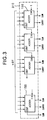
- the preferred embodiment of the multiplier circuit which is designed to perform multiplication of n-bit multiplied value and a multiplying value, has n in number of partial AND's generating portion 200, an intermediate sum generating portion 300 inputting n of partial AND's and finally generates two intermediate sums, and a carry propagation type adder 500 of two inputs for adding two intermediate sums output from the intermediate sum generating portion 300.
- the intermediate sum generating portion 300 is constructed by connecting a first stage intermediate sum calculating circuits 310..., second stage intermediate sum calculating circuits 320..., a final stage intermediate sum calculating circuit 400 in a multi-stage tree configuration.
- Each of the intermediate sum calculating circuits 310, 320, ... 400 are formed employing the adders discussed with respect to Fig. 1.
- Each of the first stage intermediate sum calculating circuits 310 receives four partial AND's from the partial AND generating portion 200 and derives two intermediate sums for outputting.
- the second stage intermediate sum calculating circuits 320 receives respective two outputs of two first stage intermediate sum calculating circuits 310 and thus four outputs of the first stage intermediate sum calculating circuits to outputs two outputs.
- Number of the intermediate sum calculating circuits at respective stages is determined corresponding to number of bits of the multiplying value. Also, the number of stages of the intermediate sum calculating circuits to be employed in the intermediate sum generating portion is determined from (log n - log 2)/(log 2). For instance, if the multiplying value is 16 bits, the number of stages of the intermediate sum calculating circuits becomes three. In this case, number of the intermediate sum calculating circuits 310 in the first stage becomes 4, number of the intermediate sum calculating circuit 320 in the second stage becomes 2, and number of the intermediate sum calculating circuit 400 at the final stage becomes 1.
- the intermediate sum calculating circuit 310, 320, ... 400 employing the adder 150 of four inputs and two outputs as illustrated in Fig. 1, will be discussed with reference to Fig. 3.
- the intermediate sum calculating circuit is constructed with n or more in number of adders 150 when the multiplied value is n bits.
- the intermediate carry cout of each adder 150 is connected to carry input cin of the adder 150 of the next digit for establishing parallel connection. To the carry input cin of the adder 150 at the lowermost digit, "0" is input.
- the intermediate carry of the adder 150 at the uppermost digit is used as SUM.
- Number of the adders 150 employed in each intermediate sum calculating circuit is n + 3 in the first stage adder series, increased toward the upper stage and finally becomes 2n at the final stage, when the multiplied value is n-bit, for example.
- D (cout) is calculated from (X, Y, Z, W) at the lowermost digit and D is further calculated from (X, Y, Z, W, D) in subsequent digits.
- D (cout) is calculated only from (X, Y, Z, W) and will not be influenced by D (cout) of the preceding digit. Therefore, even at a large number of digits, it does not take a long period.
- n in number of n-bit partial AND's A(1) to A(n) are derived. Accordingly, n in number of the partial AND's A(1) to A(n) are output from each of the partial AND generating portions 200. Number of the partial AND's to be generated by the partial AND generating portion 200 depends on number of bits of the multiplying value Y.
- number of bits of the partial AND's depends on number of bits of the multiplied value X. Accordingly, assuming the multiplied value X is 8-bit and multiplying value Y is 16-bit, 16 8-bits partial AND's are output from the partial AND generating portion 200.
- each first stage intermediate sum calculating circuit 310 For each of a plurality of first stage intermediate sum calculating circuits 310 ...., four in number of partial AND's are input. Each first stage intermediate sum calculating circuit 310.... then performs addition for the four partial AND's input thereto and outputs two intermediate sums. By this, the number of the intermediate sums output from the first stage intermediate sum calculating circuits 310... becomes half (1/2 n) of the number of the partial AND's from the partial AND generating portion 200.
- Respective four intermediate sums output from the first stage intermediate sum calculating circuits 310.... are input to corresponding second stage intermediate sum calculating circuits 320....
- four intermediate sums from the first stage intermediate sum calculating circuits 310... are added to be output as two second stage intermediate sums. Therefore, through the second stage intermediate sum calculating portions 320...., number of the intermediate sums output therefrom becomes quarter (1/4 n) of the number of the partial AND's input from the partial AND generating portion 200.
- the number of stages of the intermediate sum calculating circuits becomes (log n - log 2)/(log 2) which is much smaller than (log n - log 2)/(log 1.5) which is required when the conventional intermediate sum calculating circuits employing full adders of three input and two output.
- a necessary period to reduce the number of the intermediate sums into two employing the adders of four inputs and two outputs is expressed as follow with assuming that the delay period of the adder is ⁇ 4.
- the necessary period to reduce the number of the intermediate sums into two in the conventional Wallace type multiplier circuit is expressed as follows with assuming that the delay period of the full adder is ⁇ 3.
- the delay period ⁇ 4 of the adder employed in the preferred embodiment satisfies the equation ⁇ 4 ⁇ ⁇ 3 x log 2 ⁇ log 1.5 ⁇ ⁇ 3 x 1.7 the multiplier circuit can be speeded up.
- the adder employed in the preferred embodiment satisfies the foregoing condition. Therefore, the preferred embodiment of the multiplier circuit according to the present invention can provide higher speed than the conventional Wallace type multiplier circuit employing the full adders of three inputs and two outputs.
- the present invention can speed up the period required for reducing the number of intermediate sums, which is the substantial part of operation period of the multiplier circuit, it becomes possible to significantly speed up the operation speed of the multiplier circuit.
Landscapes
- Physics & Mathematics (AREA)
- General Physics & Mathematics (AREA)
- Engineering & Computer Science (AREA)
- Computational Mathematics (AREA)
- Mathematical Analysis (AREA)
- Pure & Applied Mathematics (AREA)
- Theoretical Computer Science (AREA)
- Mathematical Optimization (AREA)
- Computing Systems (AREA)
- General Engineering & Computer Science (AREA)
- Mathematical Physics (AREA)
- Complex Calculations (AREA)
Applications Claiming Priority (3)
| Application Number | Priority Date | Filing Date | Title |
|---|---|---|---|
| JP3104293 | 1993-02-22 | ||
| JP31042/93 | 1993-02-22 | ||
| JP5031042A JPH06242928A (ja) | 1993-02-22 | 1993-02-22 | 加算器およびこれを用いた乗算回路 |
Publications (2)
| Publication Number | Publication Date |
|---|---|
| EP0613082A1 true EP0613082A1 (fr) | 1994-08-31 |
| EP0613082B1 EP0613082B1 (fr) | 2000-05-10 |
Family
ID=12320434
Family Applications (1)
| Application Number | Title | Priority Date | Filing Date |
|---|---|---|---|
| EP94102668A Expired - Lifetime EP0613082B1 (fr) | 1993-02-22 | 1994-02-22 | Additioneur 4:2 et circuit multiplieur utilisant celui-ci |
Country Status (4)
| Country | Link |
|---|---|
| US (1) | US5426598A (fr) |
| EP (1) | EP0613082B1 (fr) |
| JP (1) | JPH06242928A (fr) |
| DE (1) | DE69424329T2 (fr) |
Cited By (4)
| Publication number | Priority date | Publication date | Assignee | Title |
|---|---|---|---|---|
| EP0673171A3 (fr) * | 1994-03-17 | 1996-11-06 | Ibm | Décodeur vidéo. |
| WO2001075587A3 (fr) * | 2000-03-31 | 2002-01-24 | Intel Corp | Architecture de multiplicateur dans un processeur polyvalent optimise en vue d'addition a entrees multiples efficace |
| EP1271474B1 (fr) * | 2001-06-25 | 2011-11-02 | NEC Corporation | Bloc fonctionnel |
| CN111106825A (zh) * | 2018-10-25 | 2020-05-05 | Arm 有限公司 | 数据压缩器逻辑电路 |
Families Citing this family (19)
| Publication number | Priority date | Publication date | Assignee | Title |
|---|---|---|---|---|
| US5644520A (en) * | 1995-05-31 | 1997-07-01 | Pan; Shao Wei | Accumulator circuit and method of use thereof |
| US6385634B1 (en) * | 1995-08-31 | 2002-05-07 | Intel Corporation | Method for performing multiply-add operations on packed data |
| US7395298B2 (en) * | 1995-08-31 | 2008-07-01 | Intel Corporation | Method and apparatus for performing multiply-add operations on packed data |
| JP3678512B2 (ja) * | 1996-08-29 | 2005-08-03 | 富士通株式会社 | 乗算回路、該乗算回路を構成する加算回路、該乗算回路の部分積ビット圧縮方法、および、該乗算回路を適用した大規模半導体集積回路 |
| US6125379A (en) * | 1998-02-11 | 2000-09-26 | The Research Foundation Of State University Of New York | Parallel VLSI shift switch logic devices |
| US6233671B1 (en) | 1998-03-31 | 2001-05-15 | Intel Corporation | Staggering execution of an instruction by dividing a full-width macro instruction into at least two partial-width micro instructions |
| US6230257B1 (en) * | 1998-03-31 | 2001-05-08 | Intel Corporation | Method and apparatus for staggering execution of a single packed data instruction using the same circuit |
| US6230253B1 (en) * | 1998-03-31 | 2001-05-08 | Intel Corporation | Executing partial-width packed data instructions |
| US6192467B1 (en) | 1998-03-31 | 2001-02-20 | Intel Corporation | Executing partial-width packed data instructions |
| US6523049B1 (en) * | 1999-12-21 | 2003-02-18 | International Business Machines Corporation | Circuit and method for determining greater than or equal to three out of sixty-six |
| US6742011B1 (en) * | 2000-02-15 | 2004-05-25 | Hewlett-Packard Development Company, L.P. | Apparatus and method for increasing performance of multipliers utilizing regular summation circuitry |
| US7430578B2 (en) * | 2001-10-29 | 2008-09-30 | Intel Corporation | Method and apparatus for performing multiply-add operations on packed byte data |
| US6921477B2 (en) * | 2002-04-08 | 2005-07-26 | Steven L. Wilhelm | Groundwater treatment system and method |
| US7156988B2 (en) * | 2003-05-16 | 2007-01-02 | Wilhelm Steven L | Floating product removal |
| KR101061906B1 (ko) * | 2004-02-19 | 2011-09-02 | 삼성전자주식회사 | 전력분석공격에 안전한 기본 연산 장치 및 방법 |
| US8554823B2 (en) * | 2010-09-02 | 2013-10-08 | Texas Instruments Incorporated | Technique for optimization and re-use of hardware in the implementation of instructions used in viterbi and turbo decoding, using carry and save arithmetic |
| RU2586565C2 (ru) * | 2011-12-20 | 2016-06-10 | Лев Петрович Петренко | ФУНКЦИОНАЛЬНАЯ СТРУКТУРА ПРЕДВАРИТЕЛЬНОГО СУММАТОРА f1(ΣCD) УСЛОВНО "j" РАЗРЯДА ПАРАЛЛЕЛЬНО-ПОСЛЕДОВАТЕЛЬНОГО УМНОЖИТЕЛЯ fΣ(Σ), РЕАЛИЗУЮЩАЯ ПРОЦЕДУРУ "ДЕШИФРИРОВАНИЯ" АРГУМЕНТОВ ЧАСТИЧНЫХ ПРОИЗВЕДЕНИЙ СО СТРУКТУРАМИ АРГУМЕНТОВ МНОЖИМОГО [mj]f(2n) И МНОЖИТЕЛЯ [ni]f(2n) В ПОЗИЦИОННОМ ФОРМАТЕ "ДОПОЛНИТЕЛЬНОГО КОДА" И ФОРМИРОВАНИЯ ПРОМЕЖУТОЧНОЙ СУММЫ [1,2Sjh1]f(2n) В ПОЗИЦИОННОМ ФОРМАТЕ "ДОПОЛНИТЕЛЬНОГО КОДА RU" (ВАРИАНТЫ РУССКОЙ ЛОГИКИ) |
| US9383763B1 (en) | 2014-01-03 | 2016-07-05 | Altera Corporation | Multimode current mirror circuitry |
| WO2017037880A1 (fr) * | 2015-09-01 | 2017-03-09 | 日本電気株式会社 | Modulateur δς, émetteur et intégrateur |
Family Cites Families (5)
| Publication number | Priority date | Publication date | Assignee | Title |
|---|---|---|---|---|
| US4901270A (en) * | 1988-09-23 | 1990-02-13 | Intel Corporation | Four-to-two adder cell for parallel multiplication |
| JP2518548B2 (ja) * | 1990-10-17 | 1996-07-24 | 富士通株式会社 | 多入力加算回路 |
| JPH04250527A (ja) * | 1991-01-28 | 1992-09-07 | Nec Corp | 演算回路 |
| US5210711A (en) * | 1992-02-26 | 1993-05-11 | Sony Corporation Of America | Very fast variable input multi-bit adder |
| US5303176A (en) * | 1992-07-20 | 1994-04-12 | International Business Machines Corporation | High performance array multiplier using four-to-two composite counters |
-
1993
- 1993-02-22 JP JP5031042A patent/JPH06242928A/ja active Pending
-
1994
- 1994-02-22 EP EP94102668A patent/EP0613082B1/fr not_active Expired - Lifetime
- 1994-02-22 DE DE69424329T patent/DE69424329T2/de not_active Expired - Lifetime
- 1994-02-22 US US08/199,655 patent/US5426598A/en not_active Expired - Lifetime
Non-Patent Citations (2)
| Title |
|---|
| G. GOTO ET AL.: "A 54 x 54-b Regularly Structured Tree Multiplier", IEEE JOURNAL OF SOLID-STATE CIRCUITS., vol. 27, no. 9, September 1992 (1992-09-01), NEW YORK US, pages 1229 - 1235, XP000311186 * |
| M. SANTORO ET AL.: "SPIM: A Pipelined 64 x 64-bit Iterative Multiplier", IEEE JOURNAL OF SOLID-STATE CIRCUITS., vol. 24, no. 2, April 1989 (1989-04-01), NEW YORK US, pages 487 - 493, XP000124892 * |
Cited By (4)
| Publication number | Priority date | Publication date | Assignee | Title |
|---|---|---|---|---|
| EP0673171A3 (fr) * | 1994-03-17 | 1996-11-06 | Ibm | Décodeur vidéo. |
| WO2001075587A3 (fr) * | 2000-03-31 | 2002-01-24 | Intel Corp | Architecture de multiplicateur dans un processeur polyvalent optimise en vue d'addition a entrees multiples efficace |
| EP1271474B1 (fr) * | 2001-06-25 | 2011-11-02 | NEC Corporation | Bloc fonctionnel |
| CN111106825A (zh) * | 2018-10-25 | 2020-05-05 | Arm 有限公司 | 数据压缩器逻辑电路 |
Also Published As
| Publication number | Publication date |
|---|---|
| EP0613082B1 (fr) | 2000-05-10 |
| US5426598A (en) | 1995-06-20 |
| DE69424329T2 (de) | 2001-02-08 |
| DE69424329D1 (de) | 2000-06-15 |
| JPH06242928A (ja) | 1994-09-02 |
Similar Documents
| Publication | Publication Date | Title |
|---|---|---|
| EP0613082A1 (fr) | Additioneur 4:2 et circuit multiplieur utilisant celui-ci | |
| US5956265A (en) | Boolean digital multiplier | |
| US5790446A (en) | Floating point multiplier with reduced critical paths using delay matching techniques | |
| US7395304B2 (en) | Method and apparatus for performing single-cycle addition or subtraction and comparison in redundant form arithmetic | |
| US5506799A (en) | Booth array multiplying circuit having carry correction | |
| JP2000347836A (ja) | 高次基数除算器およびその方法 | |
| JP2000259394A (ja) | 浮動小数点乗算器 | |
| EP0356153B1 (fr) | Procédé et appareil de division en base 2**n à sélection chevauchée de bits de quotient, et arrondissement et correction simultanés de quotient | |
| US5132925A (en) | Radix-16 divider using overlapped quotient bit selection and concurrent quotient rounding and correction | |
| US5161119A (en) | Weighted-delay column adder and method of organizing same | |
| CN1108557C (zh) | 减少高速算术单元中超前进位加法器级数的结构和方法 | |
| US4677583A (en) | Apparatus for decimal multiplication | |
| US5586071A (en) | Enhanced fast multiplier | |
| US4823300A (en) | Performing binary multiplication using minimal path algorithm | |
| JPH0312738B2 (fr) | ||
| JP2830566B2 (ja) | 十進数乗算器 | |
| JPH05158659A (ja) | 乗算器 | |
| JPH0793134A (ja) | 乗算器 | |
| US20060277242A1 (en) | Combining circuitry | |
| JP2606326B2 (ja) | 乗算器 | |
| Tamilselvan et al. | An efficient MAC design for image processing application | |
| JP2765516B2 (ja) | 積和演算器 | |
| EP0626638A1 (fr) | Additionneur en complément à un et méthode opératoire | |
| US20040143619A1 (en) | Sparce-redundant fixed point arithmetic modules | |
| JP2705640B2 (ja) | 積和演算器 |
Legal Events
| Date | Code | Title | Description |
|---|---|---|---|
| PUAI | Public reference made under article 153(3) epc to a published international application that has entered the european phase |
Free format text: ORIGINAL CODE: 0009012 |
|
| AK | Designated contracting states |
Kind code of ref document: A1 Designated state(s): DE FR GB |
|
| 17P | Request for examination filed |
Effective date: 19941108 |
|
| 17Q | First examination report despatched |
Effective date: 19980608 |
|
| GRAG | Despatch of communication of intention to grant |
Free format text: ORIGINAL CODE: EPIDOS AGRA |
|
| GRAG | Despatch of communication of intention to grant |
Free format text: ORIGINAL CODE: EPIDOS AGRA |
|
| GRAG | Despatch of communication of intention to grant |
Free format text: ORIGINAL CODE: EPIDOS AGRA |
|
| GRAH | Despatch of communication of intention to grant a patent |
Free format text: ORIGINAL CODE: EPIDOS IGRA |
|
| GRAH | Despatch of communication of intention to grant a patent |
Free format text: ORIGINAL CODE: EPIDOS IGRA |
|
| GRAA | (expected) grant |
Free format text: ORIGINAL CODE: 0009210 |
|
| AK | Designated contracting states |
Kind code of ref document: B1 Designated state(s): DE FR GB |
|
| REF | Corresponds to: |
Ref document number: 69424329 Country of ref document: DE Date of ref document: 20000615 |
|
| ET | Fr: translation filed | ||
| PLBE | No opposition filed within time limit |
Free format text: ORIGINAL CODE: 0009261 |
|
| STAA | Information on the status of an ep patent application or granted ep patent |
Free format text: STATUS: NO OPPOSITION FILED WITHIN TIME LIMIT |
|
| 26N | No opposition filed | ||
| REG | Reference to a national code |
Ref country code: GB Ref legal event code: IF02 |
|
| PGFP | Annual fee paid to national office [announced via postgrant information from national office to epo] |
Ref country code: FR Payment date: 20100223 Year of fee payment: 17 |
|
| PGFP | Annual fee paid to national office [announced via postgrant information from national office to epo] |
Ref country code: GB Payment date: 20100202 Year of fee payment: 17 Ref country code: DE Payment date: 20100303 Year of fee payment: 17 |
|
| GBPC | Gb: european patent ceased through non-payment of renewal fee |
Effective date: 20110222 |
|
| REG | Reference to a national code |
Ref country code: FR Ref legal event code: ST Effective date: 20111102 |
|
| REG | Reference to a national code |
Ref country code: DE Ref legal event code: R119 Ref document number: 69424329 Country of ref document: DE Effective date: 20110901 |
|
| PG25 | Lapsed in a contracting state [announced via postgrant information from national office to epo] |
Ref country code: FR Free format text: LAPSE BECAUSE OF NON-PAYMENT OF DUE FEES Effective date: 20110228 |
|
| PG25 | Lapsed in a contracting state [announced via postgrant information from national office to epo] |
Ref country code: GB Free format text: LAPSE BECAUSE OF NON-PAYMENT OF DUE FEES Effective date: 20110222 |
|
| PG25 | Lapsed in a contracting state [announced via postgrant information from national office to epo] |
Ref country code: DE Free format text: LAPSE BECAUSE OF NON-PAYMENT OF DUE FEES Effective date: 20110901 |