EP0615202A2 - Appareil et procédé de convertir une description logique - Google Patents
Appareil et procédé de convertir une description logique Download PDFInfo
- Publication number
- EP0615202A2 EP0615202A2 EP94103530A EP94103530A EP0615202A2 EP 0615202 A2 EP0615202 A2 EP 0615202A2 EP 94103530 A EP94103530 A EP 94103530A EP 94103530 A EP94103530 A EP 94103530A EP 0615202 A2 EP0615202 A2 EP 0615202A2
- Authority
- EP
- European Patent Office
- Prior art keywords
- logic
- register
- descriptions
- input
- long
- Prior art date
- Legal status (The legal status is an assumption and is not a legal conclusion. Google has not performed a legal analysis and makes no representation as to the accuracy of the status listed.)
- Granted
Links
Images


Classifications
-
- G—PHYSICS
- G06—COMPUTING OR CALCULATING; COUNTING
- G06F—ELECTRIC DIGITAL DATA PROCESSING
- G06F30/00—Computer-aided design [CAD]
- G06F30/30—Circuit design
Definitions
- the present invention relates to a logic description conversion apparatus for and a logic description conversion method of converting a logic description into a more accurate logic description.
- optimum logic is synthesized from a logic description by register extraction means for extracting a corresponding register, Boolean means for processing the logic description by Boolean computation and logic optimization means for optimizing, based on circuit information and timing information for logic optimization, the Boolean logic descriptions which were created by the Boolean means.
- the register extraction means extracts a part of logic descriptions which is described in the register format as a register.
- the Boolean means processes logic descriptions which are sandwitched between registers or included in a range which is partitioned by input/output ports, that is, logic descriptions other than registers.
- the logic optimization means optimizes the logic in accordance with the circuit information and the timing information for logic optimization, to thereby generate a logic circuit having optimized logic descriptions.
- Fig. 18 shows a circuit which operates at the timing which is shown in Fig. 17.
- CLK is a clock input and indicated at DATAIN is a data input.
- An input control logic group 11 is a logic group which includes ST[0] to ST[3] of Fig. 18.
- Indicated at reference numeral 12 is a logic group which includes the functionlogic ALU while indicated at reference numeral 13 is a logic group which is controlled by the input control logic ST[0].
- the registers reg-A and reg-B are basically formed in the D-flip-flop structure.
- the reference operation clock for the logic circuit shown in Fig. 18 is the one-clock T.
- the logic group 12 includes the functionlogic ALU of the data computation family and a selector 14 controlled by the input control logic ST[3] of the control computation family.
- the selector 14 selects one of signals which are received from input parts P2 and P3 and outputs the selected signal to a D-input of the register reg-B .
- the signal which is obtainable from the input part P2 is a Q-output of the register reg-B
- the signal which is obtainable from the input part P3 is a computation result of the fuctionlogic ALU .
- the long-term logic input register information consists of a name which specifies the extracted register, information about the input control logic of the extracted register and input data to be given to the extracted register.
- the logic description providing means comprises first memory means in which the first logic descriptions are stored and the long-term logic input register information providing means comprises second memory means in which the long-term logic input register information is stored.
- the logic description conversion apparatus further comprises third memory means for temporarily storing the extracted register input control information.
- the logic description conversion apparatus is formed by a microcomputer
- the extracted register input control information generating means is a CPU which operates in accordance with a preliminarily prepared first program
- the logic description conversion means is the CPU which operates in accordance with a preliminarily prepared second program.
- the logic description conversion apparatus may further comprise fourth memory means in which the first and the second programs are stored.
- the first and the second memory means are RAMs
- the third memory means is a hard disk
- the fourth memory means is a ROM
- the first, the second and the fourth memory means and the CPU are formed as one computation processing part of single chip.
- the present invention is also directed to a logic description conversion method of converting logic descriptions from which a logic circuit will be formed by logic synthesis into higher level logic descriptions from which a logic circuit as it is exactly defined in specifications will be created.
- the method comprises the steps of: (a) extracting a description which will serve as a register from the first logic descriptions as an extracted register and for generating extracted register input control information in which the extracted register is made correspondence to input control logic which designates an input timing and the like for the extracted register; and (b) based on long-term logic input register information, which designates a register which has the long-term operation logic part at a receiving side of registers which are defined by the first logic descriptions as a long-term logic input register, and the extracted register input control information, converting the first logic descriptions into second logic descriptions in which the input control logic of the long-term logic input register and the long-term operation logic part of a receiving side of the long-term logic input register are logically separated from each other.
- the step (a) comprises the steps of: (a-1) extracting a description which will serve as a register from the first logic descriptions as an extracted register; (a-2) extracting information about the input control logic of the extracted register; (a-3) extracting input data to be given to the extracted register; and (a-4) outputting the extracted register input control information in which the extracted register, the information about the input control logic ad the input data are stored as a set.
- the logic description conversion means converts the first logic descriptions into the second logic descriptions, in which the input control logic of the long-term logic input register and the long-term operation logic part of a receiving side of the long-term logic input register are logically separated from each other, based on long-term logic input register information and the extracted register input control information.
- logic synthesis will not be performed with the input control logic and the long-term operation logic part having different operation clocks existing mixed.
- the second logic descriptions include a long-term operation logic part which operates at an operation clock which is longer than a reference operation clock, a logic circuit will be accurately synthesized from the second logic descriptions by logic synthesis.
- the first logic descriptions are converted into second logic descriptions in which the input control logic of the long-term logic input register and the long-term operation logic part of a receiving side of the long-term logic input register are logically separated from each other.
- the second logic descriptions include a long-term operation logic part which operates at an operation clock which is longer than a reference operation clock, a logic circuit will be accurately synthesized from the second logic descriptions by logic synthesis.
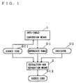
- Fig. 1 is a block diagram showing the structure of a logic description conversion apparatus according to a preferred embodiment of the present invention.
- conversion-into-table means 1 receives a source code SC1 and generates a reference table D1.
- the source code SC1 is a source code which is formed by logic descriptions which include a multi-clock transfer path which requires longer time than a one-clock frequency, or a reference operation clock, in performing register-to-register data transfer.
- the reference table D1 is memory means in which register input control information is registered which consists of a register name, an input control condition of a register which is defined by the register name and an input data name which corresponds to the input control condition.
- Extraction and separation means 2 converts the source code SC1 based on an indicator D2 which is inputted in advance and the reference table D1 and generates a source code SC2 which consists of sophisticated logic descriptions from which a logic circuit as it is defined by the specifications.
- the indicator D2 is memory means in which long-term logic input register information, i.e., the name of a receiving side register of the multi-clock transfer path is registered.
- the source code SC2 is a source code which separately lists a logic description which consists of the receiving side register of the multi-clock transfer path and input control for this register and a logic description which does not include the receiving side register of the multi-clock transfer path.
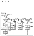
- Fig. 2 is a flow chart showing a logic description conversion method which is performed by the logic description conversion apparatus of Fig. 1.
- Fig. 5 is a flow chart showing an example of logic descriptions of the source code SC1.
- a rising (falling) edge of a clock input CLK is detected.
- input control logic ST (ST[0] to ST[3]) are checked at steps S11, S21, S31 and S41.
- steps S11, S21, S31 and S41 are checked at steps S11, S21, S31 and S41.
- either one of the input control logic ST is enabled (i.e., becomes "H").
- either one of the steps S11, S21, S31 and S41 is judged as enable ( yes ).
- step S11 If yes at the step S11, the sequence proceeds to steps S12 to S15.
- step S12 input data DATAIN are entered in the register reg-A and at the step S13, stored data of the register reg-B are held as they are.
- step S14 execution of the functionlogic ALU computation is started based on the stored data stored in the register reg-A (namely, input data DATAIN). Similarly to the conventional technique, the computation of the functionlogic ALU is performed at the three-clock frequency 3T which is longer than the frequency of the reference operation clock (one-clock T).
- step S15 ST[3] to ST[0] are respectively set at "0,” "0,” “1” and "0.” In other words, upon completion of the steps S12 to S15, by setting ST[1] at "1," execution of steps S22 to S24 is called for.
- step S22 the stored data of the register reg-A are held as they presently are, and the stored data of the register reg-B are held as they presently are at the step S23, followed by the step S24 at which ST[3] to ST[0] are respectively set at "0,” "1,” "0” and "0.” That is, after completion of the steps S22 to S24, execution of steps S32 to S34 is called for by setting the ST[2] at "1.”
- step S32 the stored data of the register reg-A are held as they presently are, and the stored data of the register reg-B are held as they presently are at the step S33, followed by the step S34 at which ST[3] to ST[0] are respectively set at "1," "0,” "0" and "0.” That is, after completion of the steps S32 to S34, execution of steps S42 to S44 is called for by setting the ST[3] at "1.”
- step S42 If yes at the step S41, at the step S42, the stored data of the register reg-A are held as they presently are, and the computation result of the data computation functionlogic ALU is stored in the register reg-B at the step S43, followed by the step S44 at which ST[3] to ST[0] are respectively set at "0,” "0,” “0” and "1.” That is, after completion of the steps S42 to S44, execution of steps S12 to S15 is called for by setting the ST[0] at "1.”
- the logic circuit which is imaged (i.e., synthesized) using the source code SC1 as it is shown in the flow chart is the logic circuit of Fig. 18 which shows the conventional technique.
- the selector 14, the control computation family of the register reg-B in which the multi-clock transfer path is located at the receiving side, and the functionlogic ALU both exist in the same logic group 12.
- the selector 14 which operates at one clock and the functionlogic ALU which operates at three clocks exist mixed.
- a resulting logic circuit is very likely to be different from what is intended by the circuit designer.
- the conversion-into-table means 1 detects a register from logic descriptions which are defined by the source code SC1. For instance, in the logic circuit of Fig. 18, the registers reg-A and reg-B are detected.
- the conversion-into-table means 1 extracts the input control conditions of the respective registers which were extracted at the step S1.
- the input control conditions define various conditions such as a timing at which the registers receive the input data.
- the conversion-into-table means 1 further extracts input data which correspond to the input control conditions of the respective registers.
- the input data to be given to the register reg-A are the input data DATAIN while the input data to be given to the registe r reg-A are the functionlogic ALU .
- the conversion-into-table means 1 registers extracted register input control information, which consists of the names of the registers which were extracted, the input control conditions (of the respective registers) and the input data (which correspond to the input control conditions), in the reference table D1.
- the register data of the register reg-B of the logic circuit of Fig. 18 are registered in the reference table D1 in the form as that shown in Fig. 6.
- the symbol "1' b1" shown as the input control condition represents 1-bit data "1.”
- the extraction and separation means 2 converts the logic descriptions of the source code SC1 based on the reference table D1 and the indicator D2 and generates the source code SC2 which consists of sophisticated logic descriptions from which a logic circuit as it is exactly defined by the specifications. Detailed explanation will be given below.
- the indicator D2 is information which specifies a long-term logic input register which has a multi-clock transfer path at the receiving side as shown in Fig. 4.
- the indicator D2 is registered manually in advance.
- the register reg-B is a receiving side register of the multi-clock transfer path, i.e., the data computation functionlogic ALU , as shown in Fig. 7, the name of the register reg-B is registered as a long-term logic input register in the indicator D2.
- the extraction and separation means 2 converts the logic circuit which is defined by the source code SC1 into the source code SC2 which consists of logic descriptions in which a first partial logic circuit which is formed by the receiving side register of the multi-clock transfer path and the input control logic of the same and a second partial logic circuit which includes the long-term operation logic part, i.e., the multi-clock transfer path.
- the source code SC1 shown in the flow chart of Fig. 5 defines the logic circuit of Fig. 18
- the source code SC1 is converted into the source code SC2 which defines the logic circuit of Fig. 10 in accordance with the flow charts of Figs. 8 and 9.
- a rising (falling) edge of the clock input CLK is detected.
- input control logic ST (ST[0] to ST[3]) are checked at steps S111, S121, S131 and S141. Since one of the input control logic ST is enabled ("H") at the timing shown in Fig. 17, one of the steps S111, S121, S131 and S141 is always judged enable ( yes ).
- step S111 If yes at the step S111, the sequence proceeds to steps S112 to S114.
- step S112 the input data DATAIN are shifted into the register reg-A , and at the subsequent step S113, execution of computation based on the functionlogic ALU is started based on the stored data of the register reg-A (namely, the input data DATAIN).
- step S114 ST[3] to ST[0] are respectively set at “0" "0" "1" and "0.” That is, after completion of the steps S112 to S114, execution of steps S122 to S123 is instructed by setting ST[1] at "1.”
- step S122 the stored data of the register reg-A are held as they presently are.
- step S123 ST[3] to ST[0] are respectively set at "0,” "1,” "0” and "0.” That is, after completion of the steps S122 to S124, execution of steps S132 to S133 is instructed by setting ST[2] at "1.”
- step S132 the stored data of the register reg-A are held as they presently are.
- step S133 ST[3] to ST[0] are respectively set at "1," "0,” “0” and "0.” That is, after completion of the steps S132 to S133, execution of steps S142 to S143 is instructed by setting ST[3] at "1.”
- step S141 If yes at the step S141, at the step S142, the stored data of the register reg-A are held as they presently are.
- step S143 ST[3] to ST[0] are respectively set at "0,” “0,” “0” and "1.” That is, after completion of the steps S142 to S144, execution of steps S112 to S114 is instructed by setting ST[0] at "1.”
- a rising (falling) edge of the clock input CLK is detected.
- the sequence proceeds to a step S201.
- step S201 the input control logic ST[3] is checked. If ST[3] is "1," the sequence proceeds to a step S202 at which the computation result of the data computation functionlogic ALU is stored in the register reg-B . The sequence then returns to the step S200.
- step S203 the sequence proceeds to a step S203 at which the content of the register reg-B is held. The sequence then returns to the step S200.
- the flow chart of Fig. 8 is a flow chart which defines the second partial logic circuit including the multi-clock transfer path, and corresponds to the partial logic circuit 3 which is shown in Fig. 10.
- the flow chart of Fig. 9 is a flow chart which defines the first partial logic circuit which is comprised of the receiving side register of the multi-clock transfer path and the input control logic for the receiving side register, and therefore, corresponds to the partial logic circuit 4 which is shown in Fig. 10.
- the logic circuit which is defined by the source code SC2 shown in Fig. 10 will be described.
- the selector 14, the control computation family of the register reg-B is formed within the partial logic circuit 4 while a data computation logic group 12' which is located at the receiving side of the register reg-B and which consists only of the data computation functionlogic ALU is formed within the partial logic circuit 3. That is, the source code SC2 is logic descriptions in which the selector 14 of the control computation family and the functionlogic ALU of the data computation family are completely separated from each other.
- the logic circuit which is defined by the source code SC2 is formed by logic descriptions in which the control computation family and the data computation family regarding the same register are completely separated from each other. Hence, in which it is possible to separately control the control computation family and the data computation family. It then follows that there is no possibility that logic synthesis will result in formation of logic which is different from what is defined by the specifications.
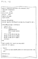
- Figs. 11 to 14 show an example of descriptions which are written in the existing hardware description language, Verilog-HDL .
- Fig. 11 shows descriptions which correspond to the logic circuit of Fig. 18,
- Fig. 12 shows descriptions which correspond to the flow chart of Fig. 8
- Fig. 13 shows descriptions which correspond to the flow chart of Fig. 9
- Fig. 14 shows descriptions which correspond to the logic circuit of Fig. 10.
- the descriptions of Fig. 14 include a module subroutineA shown in Fig. 12 and a module subroutineB shown in Fig. 13.
- the symbols "regA" and "regB” respectively represent the register reg-A and the register reg-B .
- the source code SC1 in which the control computation family and the data computation family relevant to the register reg-B exist mixed altogether as can be seen at mainroutineC in Fig. 11, is converted into the source code SC2 in which the module subroutineA of the control computation family and the module subroutineB of the data computation family regarding the register reg-B are completely separated from each other as can be seen at mainroutineA in Fig. 14.
- the source code SC2 is logic descriptions which can separately control the control computation family and the data computation family regarding the register reg-B , even if the operation clocks for the control computation family and the data computation family are different from each other, logic which is different from what is defined by the specification will never be synthesized by logic synthesis.
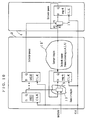
- Figs. 15 and 16 are block diagrams showing an example of application of the logic description conversion apparatus of the present invention to a microcomputer.
- the microcomputer is comprised of a one-chip computation process part 20 and a main memory 30.
- the computation process part 20 is formed by RAMs 21 and 22, a CPU 23 and a ROM 24.
- the RAM 21 is an area in which the reference table D1 is to be stored while the RAM 22 is an area in which the indicator D2 is to be stored.
- the ROM 24 stores a conversion-into-table process instruction set 25 in which the conversion-into-table method is programmed and an extraction and separation process instruction set 26 in which the extraction and separation process is programmed.
- the conversion-into-table process instruction set 25 is, as shown in Fig. 16, comprised of a register search process 41, an input control condition extraction process 42, an input control condition extraction process 43 corresponding to the input control conditions and a reference table generation process 44.
- the processes 41 to 44 each include an instruction set which corresponds to the steps S1 to S4 of the flow chart of Fig. 2.
- the separation process instruction set 26 includes an instruction set which corresponds to the step S5 of the flow chart of Fig 2.
- the main memory 30 is formed by a hard disk and functions as an area for storing the source code SC1 and the source code SC2.
- Data transfer between the CPU 23 and the internal memories 21, 22 and 24 is achieved through an internal bus 32 while data transfer between the CPU 23 and the main memory 30, or an external memory, is achieved through an external bus 31.
- the CPU 23 in accordance with an instruction which is defined in the conversion-into-table process instruction set 25, the CPU 23 enters into the RAM 21 the reference table D1 which is formed by the extracted register input control information which was obtained from the source code SC1. Further, in accordance with an instruction which is defined in the separation process instruction set 26 and in light of the reference table D1 and the indicator D2, the CPU 23 converts the source code SC1 into the source code SC2 and enters the source code SC2 in the main memory 30.
- Verilog-HDL is used as a hardware description language to write the logic descriptions of the source code SC1 in this embodiment
- the hardware description language is not limited to Verilog-HDL .
- the present invention is also applicable to where the logic descriptions of the source code SC1 are written in the language C.
Landscapes
- Engineering & Computer Science (AREA)
- Computer Hardware Design (AREA)
- Physics & Mathematics (AREA)
- Theoretical Computer Science (AREA)
- Evolutionary Computation (AREA)
- Geometry (AREA)
- General Engineering & Computer Science (AREA)
- General Physics & Mathematics (AREA)
- Devices For Executing Special Programs (AREA)
- Design And Manufacture Of Integrated Circuits (AREA)
- Image Processing (AREA)
- Logic Circuits (AREA)
Applications Claiming Priority (3)
| Application Number | Priority Date | Filing Date | Title |
|---|---|---|---|
| JP04924793A JP3172617B2 (ja) | 1993-03-10 | 1993-03-10 | 論理記述変換装置及び方法並びに論理合成方法 |
| JP49247/93 | 1993-03-10 | ||
| JP4924793 | 1993-03-10 |
Publications (3)
| Publication Number | Publication Date |
|---|---|
| EP0615202A2 true EP0615202A2 (fr) | 1994-09-14 |
| EP0615202A3 EP0615202A3 (fr) | 1995-07-19 |
| EP0615202B1 EP0615202B1 (fr) | 2002-07-24 |
Family
ID=12825530
Family Applications (1)
| Application Number | Title | Priority Date | Filing Date |
|---|---|---|---|
| EP94103530A Expired - Lifetime EP0615202B1 (fr) | 1993-03-10 | 1994-03-08 | Appareil et procédé de convertion d'une description logique |
Country Status (4)
| Country | Link |
|---|---|
| US (1) | US5530843A (fr) |
| EP (1) | EP0615202B1 (fr) |
| JP (1) | JP3172617B2 (fr) |
| DE (1) | DE69431010T2 (fr) |
Families Citing this family (6)
| Publication number | Priority date | Publication date | Assignee | Title |
|---|---|---|---|---|
| US5854926A (en) * | 1995-01-23 | 1998-12-29 | Vlsi Technology, Inc. | Method and apparatus for identifying flip-flops in HDL descriptions of circuits without specific templates |
| US5923569A (en) * | 1995-10-17 | 1999-07-13 | Matsushita Electric Industrial Co., Ltd. | Method for designing layout of semiconductor integrated circuit semiconductor integrated circuit obtained by the same method and method for verifying timing thereof |
| JPH1185810A (ja) * | 1997-09-09 | 1999-03-30 | Mitsubishi Electric Corp | 半導体集積回路の論理回路検証装置および論理回路検証装置における論理回路検証方法 |
| US6226776B1 (en) * | 1997-09-16 | 2001-05-01 | Synetry Corporation | System for converting hardware designs in high-level programming language to hardware implementations |
| US6321295B1 (en) * | 1998-03-19 | 2001-11-20 | Insilicon Corporation | System and method for selective transfer of application data between storage devices of a computer system through utilization of dynamic memory allocation |
| WO2009067538A1 (fr) * | 2007-11-19 | 2009-05-28 | Mentor Graphics Corporation | Déréférencement de pointeur dynamique et conversion en matériel statique |
Family Cites Families (12)
| Publication number | Priority date | Publication date | Assignee | Title |
|---|---|---|---|---|
| US4703435A (en) * | 1984-07-16 | 1987-10-27 | International Business Machines Corporation | Logic Synthesizer |
| US5029102A (en) * | 1987-06-08 | 1991-07-02 | International Business Machines, Corp. | Logical synthesis |
| US5146583A (en) * | 1987-09-25 | 1992-09-08 | Matsushita Electric Industrial Co., Ltd. | Logic design system for creating circuit configuration by generating parse tree from hardware description language and optimizing text level redundancy thereof |
| US4922432A (en) * | 1988-01-13 | 1990-05-01 | International Chip Corporation | Knowledge based method and apparatus for designing integrated circuits using functional specifications |
| US5067091A (en) * | 1988-01-21 | 1991-11-19 | Kabushiki Kaisha Toshiba | Circuit design conversion apparatus |
| JPH0384676A (ja) * | 1989-08-29 | 1991-04-10 | Nec Corp | 論理回路の自動合成装置 |
| JPH03185567A (ja) * | 1989-12-14 | 1991-08-13 | Nec Corp | 論理回路の合成装置 |
| US5287289A (en) * | 1990-04-13 | 1994-02-15 | Hitachi, Ltd. | Logic synthesis method |
| US5191541A (en) * | 1990-05-14 | 1993-03-02 | Sun Microsystems, Inc. | Method and apparatus to improve static path analysis of digital circuits |
| US5345393A (en) * | 1990-08-22 | 1994-09-06 | Matsushita Electric Industrial Co., Ltd. | Logic circuit generator |
| EP0520708B1 (fr) * | 1991-06-28 | 1998-07-29 | Digital Equipment Corporation | Méthode et appareil pour convertir des syntaxes abstraites de haut niveau en une forme intermédiaire |
| US5396435A (en) * | 1993-02-10 | 1995-03-07 | Vlsi Technology, Inc. | Automated circuit design system and method for reducing critical path delay times |
-
1993
- 1993-03-10 JP JP04924793A patent/JP3172617B2/ja not_active Expired - Fee Related
-
1994
- 1994-03-08 US US08/207,204 patent/US5530843A/en not_active Expired - Fee Related
- 1994-03-08 EP EP94103530A patent/EP0615202B1/fr not_active Expired - Lifetime
- 1994-03-08 DE DE69431010T patent/DE69431010T2/de not_active Expired - Fee Related
Also Published As
| Publication number | Publication date |
|---|---|
| JP3172617B2 (ja) | 2001-06-04 |
| EP0615202A3 (fr) | 1995-07-19 |
| US5530843A (en) | 1996-06-25 |
| JPH06259501A (ja) | 1994-09-16 |
| EP0615202B1 (fr) | 2002-07-24 |
| DE69431010T2 (de) | 2003-04-10 |
| DE69431010D1 (de) | 2002-08-29 |
Similar Documents
| Publication | Publication Date | Title |
|---|---|---|
| US4803636A (en) | Circuit translator | |
| US5519630A (en) | LSI automated design system | |
| US5892682A (en) | Method and apparatus for generating a hierarchical interconnection description of an integrated circuit design and using the description to edit the integrated circuit design | |
| CN113569524B (zh) | 芯片设计中基于综合网表提取时钟树的方法及应用 | |
| US7617469B2 (en) | Assertion description conversion device, method and computer program product | |
| US5530843A (en) | Logic description conversion apparatus and a logic description conversion method | |
| EP0947923A2 (fr) | Méthode de compilation, dispositif de compilation, support d'enregistrement avec programme de compilation enregistré sur celui-ci, et support d'enregistrement avec une table de conversion utilisée dans la compilation enregistrée sur celui-ci, pour génerer un programme cible conforme au type de processeur cible | |
| US5987239A (en) | Computer system and method for building a hardware description language representation of control logic for a complex digital system | |
| US6760889B2 (en) | Method for converting a logic circuit model | |
| US5065318A (en) | Method of translating a sentence including a compound word formed by hyphenation using a translating apparatus | |
| JP2001522084A (ja) | 機械語記述からisaシミュレータとアセンブラを生成する方法 | |
| US6990641B2 (en) | Integrated circuit design system and method using preprocessor which changes hardware description in accordance with configuration | |
| US20040098685A1 (en) | Multi-cycle path analyzing method | |
| US7249334B2 (en) | Method for generating timing constraints of logic circuit | |
| CN117787160B (zh) | 一种生成数字电路的硬件描述语言的方法及装置 | |
| JPH0981616A (ja) | スタティックタイミング解析装置及びその解析方法 | |
| JPH06252266A (ja) | 半導体集積回路自動設計装置 | |
| JP2967761B2 (ja) | 論理合成方法及び装置 | |
| US6654774B1 (en) | Generation of sign extended shifted numerical values | |
| US5465383A (en) | System for forming test patterns for large scale integrated circuits | |
| CN117332727A (zh) | 一种基于ast的时钟信号提取方法和系统 | |
| JPH05342295A (ja) | 論理回路設計装置 | |
| JPH06314314A (ja) | Hdl記述装置 | |
| JPH05282392A (ja) | 回路差分変更方式とその装置 | |
| JPH10269271A (ja) | 論理合成自動変換装置 |
Legal Events
| Date | Code | Title | Description |
|---|---|---|---|
| PUAI | Public reference made under article 153(3) epc to a published international application that has entered the european phase |
Free format text: ORIGINAL CODE: 0009012 |
|
| AK | Designated contracting states |
Kind code of ref document: A2 Designated state(s): DE FR GB |
|
| PUAL | Search report despatched |
Free format text: ORIGINAL CODE: 0009013 |
|
| AK | Designated contracting states |
Kind code of ref document: A3 Designated state(s): DE FR GB |
|
| 17P | Request for examination filed |
Effective date: 19950911 |
|
| 17Q | First examination report despatched |
Effective date: 20000313 |
|
| RIC1 | Information provided on ipc code assigned before grant |
Free format text: 7G 06F 17/60 A |
|
| GRAG | Despatch of communication of intention to grant |
Free format text: ORIGINAL CODE: EPIDOS AGRA |
|
| RIC1 | Information provided on ipc code assigned before grant |
Free format text: 7G 06F 17/60 A |
|
| RIC1 | Information provided on ipc code assigned before grant |
Free format text: 7G 06F 17/60 A |
|
| GRAG | Despatch of communication of intention to grant |
Free format text: ORIGINAL CODE: EPIDOS AGRA |
|
| GRAH | Despatch of communication of intention to grant a patent |
Free format text: ORIGINAL CODE: EPIDOS IGRA |
|
| GRAH | Despatch of communication of intention to grant a patent |
Free format text: ORIGINAL CODE: EPIDOS IGRA |
|
| GRAA | (expected) grant |
Free format text: ORIGINAL CODE: 0009210 |
|
| AK | Designated contracting states |
Kind code of ref document: B1 Designated state(s): DE FR GB |
|
| REG | Reference to a national code |
Ref country code: GB Ref legal event code: FG4D |
|
| REF | Corresponds to: |
Ref document number: 69431010 Country of ref document: DE Date of ref document: 20020829 |
|
| ET | Fr: translation filed | ||
| PLBE | No opposition filed within time limit |
Free format text: ORIGINAL CODE: 0009261 |
|
| STAA | Information on the status of an ep patent application or granted ep patent |
Free format text: STATUS: NO OPPOSITION FILED WITHIN TIME LIMIT |
|
| 26N | No opposition filed |
Effective date: 20030425 |
|
| PGFP | Annual fee paid to national office [announced via postgrant information from national office to epo] |
Ref country code: DE Payment date: 20070301 Year of fee payment: 14 |
|
| PGFP | Annual fee paid to national office [announced via postgrant information from national office to epo] |
Ref country code: GB Payment date: 20070307 Year of fee payment: 14 |
|
| PGFP | Annual fee paid to national office [announced via postgrant information from national office to epo] |
Ref country code: FR Payment date: 20070308 Year of fee payment: 14 |
|
| GBPC | Gb: european patent ceased through non-payment of renewal fee |
Effective date: 20080308 |
|
| REG | Reference to a national code |
Ref country code: FR Ref legal event code: ST Effective date: 20081125 |
|
| PG25 | Lapsed in a contracting state [announced via postgrant information from national office to epo] |
Ref country code: DE Free format text: LAPSE BECAUSE OF NON-PAYMENT OF DUE FEES Effective date: 20081001 |
|
| PG25 | Lapsed in a contracting state [announced via postgrant information from national office to epo] |
Ref country code: FR Free format text: LAPSE BECAUSE OF NON-PAYMENT OF DUE FEES Effective date: 20080331 |
|
| PG25 | Lapsed in a contracting state [announced via postgrant information from national office to epo] |
Ref country code: GB Free format text: LAPSE BECAUSE OF NON-PAYMENT OF DUE FEES Effective date: 20080308 |