EP0616377A2 - Halbleiter lichtemittierende Vorrichtung und Herstellungsverfahren - Google Patents
Halbleiter lichtemittierende Vorrichtung und Herstellungsverfahren Download PDFInfo
- Publication number
- EP0616377A2 EP0616377A2 EP94104012A EP94104012A EP0616377A2 EP 0616377 A2 EP0616377 A2 EP 0616377A2 EP 94104012 A EP94104012 A EP 94104012A EP 94104012 A EP94104012 A EP 94104012A EP 0616377 A2 EP0616377 A2 EP 0616377A2
- Authority
- EP
- European Patent Office
- Prior art keywords
- aluminum
- mol ratio
- emitting element
- crystal layer
- semiconductor light
- Prior art date
- Legal status (The legal status is an assumption and is not a legal conclusion. Google has not performed a legal analysis and makes no representation as to the accuracy of the status listed.)
- Granted
Links
- 239000004065 semiconductor Substances 0.000 title claims abstract description 58
- 238000000034 method Methods 0.000 title claims description 60
- 238000004519 manufacturing process Methods 0.000 title claims description 11
- 239000013078 crystal Substances 0.000 claims abstract description 80
- 229910052782 aluminium Inorganic materials 0.000 claims abstract description 63
- XAGFODPZIPBFFR-UHFFFAOYSA-N aluminium Chemical compound [Al] XAGFODPZIPBFFR-UHFFFAOYSA-N 0.000 claims abstract description 63
- 230000008569 process Effects 0.000 claims description 23
- 229910001218 Gallium arsenide Inorganic materials 0.000 claims description 13
- 239000000758 substrate Substances 0.000 claims description 10
- 238000005229 chemical vapour deposition Methods 0.000 claims description 7
- 229910052751 metal Inorganic materials 0.000 claims description 7
- 239000002184 metal Substances 0.000 claims description 7
- 239000010408 film Substances 0.000 description 79
- 239000010410 layer Substances 0.000 description 77
- 230000001681 protective effect Effects 0.000 description 47
- 239000008188 pellet Substances 0.000 description 15
- VYPSYNLAJGMNEJ-UHFFFAOYSA-N Silicium dioxide Chemical compound O=[Si]=O VYPSYNLAJGMNEJ-UHFFFAOYSA-N 0.000 description 6
- 230000015572 biosynthetic process Effects 0.000 description 6
- 230000008859 change Effects 0.000 description 6
- 230000003647 oxidation Effects 0.000 description 6
- 238000007254 oxidation reaction Methods 0.000 description 6
- 239000002019 doping agent Substances 0.000 description 4
- 239000011241 protective layer Substances 0.000 description 4
- 230000035939 shock Effects 0.000 description 4
- 229910004205 SiNX Inorganic materials 0.000 description 3
- 238000010521 absorption reaction Methods 0.000 description 3
- 238000001311 chemical methods and process Methods 0.000 description 3
- 229910052681 coesite Inorganic materials 0.000 description 3
- 229910052906 cristobalite Inorganic materials 0.000 description 3
- 230000007547 defect Effects 0.000 description 3
- 230000000694 effects Effects 0.000 description 3
- 239000000377 silicon dioxide Substances 0.000 description 3
- 235000012239 silicon dioxide Nutrition 0.000 description 3
- 229910052682 stishovite Inorganic materials 0.000 description 3
- 239000010409 thin film Substances 0.000 description 3
- 238000002834 transmittance Methods 0.000 description 3
- 229910052905 tridymite Inorganic materials 0.000 description 3
- VHUUQVKOLVNVRT-UHFFFAOYSA-N Ammonium hydroxide Chemical compound [NH4+].[OH-] VHUUQVKOLVNVRT-UHFFFAOYSA-N 0.000 description 2
- 235000011114 ammonium hydroxide Nutrition 0.000 description 2
- 230000008901 benefit Effects 0.000 description 2
- 239000003153 chemical reaction reagent Substances 0.000 description 2
- 230000006866 deterioration Effects 0.000 description 2
- 230000001788 irregular Effects 0.000 description 2
- 239000000463 material Substances 0.000 description 2
- 238000005259 measurement Methods 0.000 description 2
- 230000004048 modification Effects 0.000 description 2
- 238000012986 modification Methods 0.000 description 2
- 230000009467 reduction Effects 0.000 description 2
- 230000007480 spreading Effects 0.000 description 2
- 238000003892 spreading Methods 0.000 description 2
- 239000000126 substance Substances 0.000 description 2
- VEXZGXHMUGYJMC-UHFFFAOYSA-M Chloride anion Chemical compound [Cl-] VEXZGXHMUGYJMC-UHFFFAOYSA-M 0.000 description 1
- XUIMIQQOPSSXEZ-UHFFFAOYSA-N Silicon Chemical compound [Si] XUIMIQQOPSSXEZ-UHFFFAOYSA-N 0.000 description 1
- 230000000903 blocking effect Effects 0.000 description 1
- 238000009792 diffusion process Methods 0.000 description 1
- 238000005516 engineering process Methods 0.000 description 1
- 150000004678 hydrides Chemical class 0.000 description 1
- 230000006872 improvement Effects 0.000 description 1
- 238000001741 metal-organic molecular beam epitaxy Methods 0.000 description 1
- 229910052710 silicon Inorganic materials 0.000 description 1
- 239000010703 silicon Substances 0.000 description 1
- 238000004381 surface treatment Methods 0.000 description 1
- 238000001039 wet etching Methods 0.000 description 1
Images



Classifications
-
- H—ELECTRICITY
- H10—SEMICONDUCTOR DEVICES; ELECTRIC SOLID-STATE DEVICES NOT OTHERWISE PROVIDED FOR
- H10H—INORGANIC LIGHT-EMITTING SEMICONDUCTOR DEVICES HAVING POTENTIAL BARRIERS
- H10H20/00—Individual inorganic light-emitting semiconductor devices having potential barriers, e.g. light-emitting diodes [LED]
- H10H20/80—Constructional details
-
- H—ELECTRICITY
- H10—SEMICONDUCTOR DEVICES; ELECTRIC SOLID-STATE DEVICES NOT OTHERWISE PROVIDED FOR
- H10H—INORGANIC LIGHT-EMITTING SEMICONDUCTOR DEVICES HAVING POTENTIAL BARRIERS
- H10H20/00—Individual inorganic light-emitting semiconductor devices having potential barriers, e.g. light-emitting diodes [LED]
- H10H20/80—Constructional details
- H10H20/84—Coatings, e.g. passivation layers or antireflective coatings
-
- H—ELECTRICITY
- H10—SEMICONDUCTOR DEVICES; ELECTRIC SOLID-STATE DEVICES NOT OTHERWISE PROVIDED FOR
- H10H—INORGANIC LIGHT-EMITTING SEMICONDUCTOR DEVICES HAVING POTENTIAL BARRIERS
- H10H20/00—Individual inorganic light-emitting semiconductor devices having potential barriers, e.g. light-emitting diodes [LED]
- H10H20/80—Constructional details
- H10H20/81—Bodies
- H10H20/816—Bodies having carrier transport control structures, e.g. highly-doped semiconductor layers or current-blocking structures
-
- H—ELECTRICITY
- H10—SEMICONDUCTOR DEVICES; ELECTRIC SOLID-STATE DEVICES NOT OTHERWISE PROVIDED FOR
- H10H—INORGANIC LIGHT-EMITTING SEMICONDUCTOR DEVICES HAVING POTENTIAL BARRIERS
- H10H20/00—Individual inorganic light-emitting semiconductor devices having potential barriers, e.g. light-emitting diodes [LED]
- H10H20/80—Constructional details
- H10H20/81—Bodies
- H10H20/822—Materials of the light-emitting regions
- H10H20/824—Materials of the light-emitting regions comprising only Group III-V materials, e.g. GaP
Definitions
- the present invention relates to a semiconductor light-emitting element using an InGaAlP system mixed crystal with a high brightness as a Light Emitting Layer in a LED, and a method for fabricating this semiconductor light-emitting element, and, in particular, to a semiconductor light-emitting element with superior resistance to humidity and with a long life expectancy providing high output performance, and a method for fabricating this semiconductor light-emitting element.
- LED Light Emitting Diode
- a light-emitting layer of an InGaAlP mixed crystal system as a high brilliant LED.
- a Ga 1-x Al x As current spreading layer as a current diffusion layer
- X Al mixed Al crystals
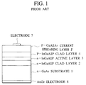
- FIG.1 is a general sectional view of an orange colored light-emitting InGaAlP LED formed using conventional technology.
- an n-type In 0.5 (Ga 0.3 Al 0.7 ) 0.5 P-clad layer 2 with a film thickness of 1.0 ⁇ m fabricated by a metal organic chemical vapor deposition method (MOCVD method) is formed on an n-type GaAs substrate 1, and then, an n-type In 0.5 (Ga 0.72 Al 0.28 ) 0.5 P active layer 3 with a film thickness of 0.5 ⁇ m, a P-type In 0.5 (Ga 0.3 Al 0.7 ) 0.5 P-clad layer 4 with a film thickness of 1.0 ⁇ m, and a P-type Ga 0.2 Al 0.8 As current spreading layer 5 with a film thickness of 10 ⁇ m are successively formed, respectively.
- MOCVD method metal organic chemical vapor deposition method
- an electrode 7 is formed on the P-type Ga 0.2 Al 0.8 As current diffusing layer 5 and an electrode 8 is formed on the other side of the n-type GaAs substrate 1. Finally, an element is detached by means of a dicing process to obtain an LED pellet.
- the Al mixed crystal ratio X Al for the Ga 1-x Al x As current diffusing layer 5 is reduced to 0.5 or less during the formation of the layer, the life expectancy of the element is improved, but, conversely, there is a large absorption ratio for the light-emitting wave lengths from red to green, therefore this is not practical.
- the natural oxidation film obtained by this method is highly irregular, even when a method to form a natural oxidation film using a chemical process is utilized, and this film lacks mechanical strength. There is therefore the drawback that variations are produced in the life expectancy.
- this chemical surface process requires another process in addition to the formation of each layer of the semiconductor light-emitting element. There is therefore the problem that excessive time is required for fabricating.
- an object of the present invention is, with due consideration to the drawbacks of such conventional semiconductor light emitting devices, to provide a semiconductor light-emitting element using an InGaAlP system mixed crystal as a light emitting layer with superior resistance to humidity and high output characteristics, and to provide a highly efficient method for fabricating this semiconductor light-emitting element.
- a semiconductor light-emitting element in a preferred embodiment according to the present invention comprises: a crystal layer formed from aluminum of a high mol ratio of 60% or greater on the light producing surface, wherein a conductive crystal with aluminum of a mol ratio of 50% or less, or a conductive crystal containing no aluminum is formed on the high aluminum crystal layer.
- the film thickness of the crystal layer In 0.5 (Ga 1-x Al x ) 0.5 P with aluminum of a mol ratio of 50% or less is within the range of 0.01 ⁇ m to 2 ⁇ m.
- Ga 1-x Al x As (where 0 ⁇ x ⁇ 0.5) is used as the crystal layer with aluminum of a mol ratio of 50% or less.
- Ga 1-x Al x As (where 0 ⁇ x ⁇ 0.5) is used as the crystal layer with aluminum of a mol ratio of 50% or less; and the film thickness of the crystal layer with aluminum of a mol ratio of 50% or less is 0.01 ⁇ m or greater
- Ga 1-x Al x As (where 0 ⁇ x ⁇ 0.5) is used as the crystal layer with aluminum of a mol ratio of 50% or less; and in the case where the forbidden band width of the crystal layer with aluminum of a mol ratio of 50% or less is smaller than the forbidden band width of the light-emitting layer, the film thickness of the crystal layer Ga 1-x Al x As (where 0 ⁇ x ⁇ 0.5) with aluminum of a mol ratio of 50% or less is within the range of 0.01 ⁇ m to 2 ⁇ m.
- a process for manufacturing a semiconductor light-emitting element of another preferred embodiment accorcing to the present invention comprises; a step for forming a crystal layer formed from aluminum of a high mol ratio of 60% or greater on the light producing surface; and a step for forming a conductive crystal with aluminum of a mol ratio of 50% or less, or a conductive crystal including no aluminum, on the high aluminum crystal layer, subsequent to the foregoing step, wherein each of the above-mentioned crystal layers is formed using a gass phase growth method.
- MOCVD metal organic chemical vapor deposition
- MBE molecular beam epitaxial growth
- the crystal layer formed from aluminum of a high mol ratio of 60% or greater is formed on a GaAs substrate.
- a group III to V crystal layer with aluminum of a mol ratio of 50% or less or containing no aluminum for example, a protective film layer 16 of In 0.5 (Ga 1-x Al x ) 0.5 P (where 0 ⁇ x ⁇ 1), Ga 1-y Al y As (where 0 ⁇ y ⁇ 0.5), InP, GaP, or GaAs or the like, is formed on a GaAlAs current diffusing layer 15 which is a light producing surface.
- This protective film 16 has the function of a humidity resistant protective film.
- MOCVD metal organic chemical vapor deposition
- MBE molecular beam epitaxial growth
- the close adhesion characteristics of the GaAlAs current diffusing layer 15 and the group III to V crystal layer (protective film) 16 with aluminum of a mol ratio of 50% or less, or containing no aluminum, are strong.
- the protective film 16 with aluminum of a mol ratio of 50% or less, or containing no aluminum is a thin film there are few defects, and a semiconductor light-emitting element can be provided which is mechanically strong so that the protective film does not peel away from the shock of the dicing process when forming the pellets, or from the shock of the wire bonding process in the manufacturing process.
- the protective film is conductive it is possible to form an ohmic electrode without the necessity of forming an opening in the protective film when it is required to form an ohmic electrode such as an SiO2, SiN x protective film or a group III to V crystal protective film with low carrier density and high resistance, or when it is required to provide a wire bonding section.
- the protective film it is possible to avoid a complicated pellet forming operation, and it is possible to prevent the intrusion of OH ⁇ ions which have a bad influence on high Al crystals because of the ohmic electrode-protective layer boundary. Furthermore, an oxidized film, which becomes a light absorbing layer on the light producing surface, is formed with extreme difficulty so that it is possible to provide a semiconductor light-emitting element with improved humidity resistance.
- FIG.2 is a general sectional view of an embodiment of a semiconductor light-emitting element which emits yellow light (wave length approximately 590 nm) of the present invention.
- an n-type In 0.5 (Ga 0.3 Al 0.7 ) 0.5 p-clad layer 12 Si dopant, carrier density 5 x 1017cm ⁇ 3) with a film thickness of 1.0 ⁇ m fabricated by the metal organic chemical vapor deposition method (MOCVD method) or by the molecular beam epitaxial growth method (MBE method) is formed on a (100) n-type GaAs substrate 11, followed by an n-type In 0.5 (Ga 0.72 Al 0.28 ) 0.5 p active layer 13 (undoped, carrier density 1 x 1017cm ⁇ 3 or less) with a film thickness of 0.5 ⁇ m; a p-type In 0.5 (Ga 0.3 Al 0.7 ) 0.5 p-clad layer 14 (Zn dopant, carrier density 5 x 1017cm ⁇ 3) with a film thickness of 1.0 ⁇ m; then a p-type Ga 0.2 Al 0.8 As current diffusing layer 15 (Zn dopant, carrier density 1 to 2 .
- an In 0.5 (Ga 1-x Al x ) 0.5 P (where 0 ⁇ x ⁇ 1) protective film 16 (Zn dopant, carrier density 5 x 1017cm ⁇ 3) is formed with aluminum of a mol ratio of 50% or less, using the MOCVD method or the MBE method, to complete the formation of the crystals.
- the film thickness of the In 0.5 (Ga 1-x Al x ) 0.5 P (where 0 ⁇ x ⁇ 1) protective film 16 is greater than 0.01 ⁇ m, it will function as a humidity resistant protective layer, but if the film becomes too thick it cannot be ignored as a light absorbing layer for light emission, therefore, the film thickness is set at about 0.01 to 2.0 ⁇ m.
- an AuZn (Zn 3 wt%, i.e., Zn is 3% by weight) surface electrode 17 with a film thickness of 1.0 ⁇ m is formed on the In 0.5 (Ga 1-x Al x ) 0.5 P protective film 16, and an AuGe (Ge 3 wt%) surface electrode 8 with a film thickness of 1.0 ⁇ m is formed on the n-type GaAs substrate 1.
- An element is then detached using the dicing process, to complete the process of forming a pellet of the semiconductor light-emitting element.
- the In 0.5 (Ga 1-x Al x ) 0.5 P protective film 16 with aluminum of a mol ratio of 50% or less, or containing no aluminum, on the GaAlAs current diffusing layer 15 which becomes the light producing surface using the metal organic chemical vapor deposition method which is the process for growing the InGaAlP system mixed crystal layers 12, 13, 14, and 15; and by successively forming each of the layers 12, 13, 14, and 15, these layers are thinly formed with good efficiency so that the GaAlAs current diffusing layer 15 and the In 0.5 (Ga 1-x Al x ) 0.5 P protective film 16 have strong, close adherence.
- the In 0.5 (Ga 1-x Al x ) 0.5 P protective film 16 is thin with few defects, making it possible to provide a semiconductor light-emitting element which has the advantage of being mechanically strong.
- the formation of a Ga 1-y Al y As (where 0 ⁇ y ⁇ 0.5) protective film instead of the In 0.5 (Ga 1-x Al x ) 0.5 P protective film 16 provides the same effect.
- FIG.3 is a graph showing the changes in the relative light output versus elapsed time for an LED lamp under conditions of high temperature and high humidity. The effectiveness of the semiconductor light-emitting element of this embodiment will be substantiated with reference to this drawing.
- FIG.3 shows the relationship between the relative light output (%) versus the time during which current is applied, in the case of 60°C ambient temperature, 90% relative humidity, and 20 mA current flow (IF).
- a dotted line A shows the case of a conventional semiconductor light-emitting element, specifically, an InGaAlP system LED with no special process used;
- the dashed line B shows the case of applying an oxidation film process, using a mixed reagent of NH4OH and H2O2, to an InGaAlP system LED in a conventional semiconductor light-emitting element;
- the alternate short and long dash line C shows the case of a semiconductor light-emitting element InGaAlP system LED formed with the In 0.5 (Ga 1-x Al x ) 0.5 P protective film 16 with a film thickness of 0.1 ⁇ m; for the embodiment shown in FIG.2.
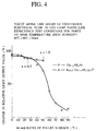
- FIG.4 is a graph showing the relationship between the Al mol ratio of a protective film on the pellet surface and the change in the relative light output values (life expectancy) for the semiconductor light-emitting element.
- the measured ambient conditions are 60°C temperature, 90% relative humidity, and 20 mA current flow (IF), and the measurements were made after current had been passed through an LED lamp produced from the semiconductor light-emitting element of the present invention for 1000 hours.
- the vertical axis represents the change in the relative light output values
- the horizontal axis represents the Al mol ratio of the pellet surface.
- the solid line shows the case for Ga 1-y Al y As and the dotted line shows the case of the In 0.5 (Ga 1-x Al x ) 0.5 P protective film.
- FIG.5 is a graph showing the relationship between the film thickness of an In 0.5 (Ga 1-x Al x ) 0.5 P protective film 16 and the change in the relative light output values (%) for this embodiment of a semiconductor light-emitting element.
- the measured ambient conditions are 60°C temperature, 90% relative humidity, and 20 mA current flow (IF), and the measurements were made after current had been passed through an LED lamp produced from the semiconductor light-emitting element of the present invention for 1000 hours.
- IF current flow
- the vertical axis represents the change in the relative light output values (%), and the horizontal axis represents the thickness [ ⁇ m]of the humidity resistant film.
- the graph shows that when the thickness of the protective film layer 16 is 0.01 ⁇ m or greater, this film functions as a humidity resistant protective layer.
- InGaAlP and GaAlAs are used as the protective film layer 16 in this embodiment.
- InP, GaAs, GaP, GaAlP, GaAsP can also be used as the protective film layer 16.
- the MOCVD method and the MBE method are used as the crystal forming methods for the light-emitting layer and the protective film layer, but, in addition to these, other methods such as an MOMBE method, a hydride VPE method, a chloride VPE method and the like can be used.
- the thickness of the protective film differs in accordance with the value of the Al mixed crystal ratio X Al .
- this thickness is in the range of 0.02 to less than 0.05 ⁇ m. Also, in the 650 nm band, this thickness differs greatly in accordance with the value of the Al mixed crystal ratio X Al , and when X Al is close to 0.7, at a thickness of 10 ⁇ m or more, almost none of the emitted light is absorbed but is nearly all is transmitted.
- the optimum value is about 2 ⁇ m or less.
- this embodiment it is possible to provide an LED with superior humidity resistance by forming a group III to V crystal with aluminum of a mol ratio of 50% or less, or containing no aluminum. Further, this embodiment was explained using an In 0.5 (Ga 1-x Al x ) 0.5 P (where 0 ⁇ x ⁇ 1) protective film 16 as the humidity-resistant protective film 16, but it is also possible to provide an LED with the same characteristics using group III to V crystals such as a Ga 1-y Al y As (where 0 ⁇ y ⁇ 0.5) crystal, or another GaAs crystal containing no Al, or InP, or the like.
- the GaAs substrate has the same characteristics as a material with a surface direction offset from a surface with a surface direction [100], or a material using a surface with a surface direction or miller indices (111), and a surface direction(110).
- each layer of the conductive type is the opposite of the conducting type in the case of the above-mentioned embodiment, that is, using the P-type rather than the n-type substrate as a GaAs substrate.
- This protective film has the function of a humidity resistant protective film, and adheres closely with strong bonding to the group III to V crystal layer with aluminum of a mol ratio of 50% or less, or containing no aluminum.
- the film of the group III to V crystal layer with aluminum of a mol ratio of 50% or less, or containing no aluminum is thin, there are few defects, and a semiconductor light-emitting element can be provided which is mechanically strong so that the protective film does not peel away from the shock of the dicing process when forming the pellets, or from the shock of the wire bonding process in the fabricating process.
- the protective film has conductive characteristics, it is possible to form an ohmic electrode without the necessity of forming an opening in the protective film, when it is required to form an ohmic electrode such as an SiO2, SiN x protective film or a group III to V crystal protective film with low carrier density and high resistance, or when it is required to provide a wire bonding section.
- the protective film it is possible to avoid a complicated pellet forming operation, and it is possible to prevent the intrusion of OH ⁇ ions which have a bad influence on high Al crystals because of the ohmic electrode - protective layer boundary.
- a highly efficient manufacturing method can be provided for a semiconductor light-emitting element. Furthermore, an oxidized film, which becomes a light absorbing layer is formed with extreme difficulty on the light producing surface, so that it is possible to provide a semiconductor light-emitting element with improved humidity resistance.
Landscapes
- Led Devices (AREA)
Applications Claiming Priority (4)
| Application Number | Priority Date | Filing Date | Title |
|---|---|---|---|
| JP5353993 | 1993-03-15 | ||
| JP53539/93 | 1993-03-15 | ||
| JP24291493A JP3264563B2 (ja) | 1993-03-15 | 1993-09-29 | 半導体発光素子及びその製造方法 |
| JP242914/93 | 1993-09-29 |
Publications (3)
| Publication Number | Publication Date |
|---|---|
| EP0616377A2 true EP0616377A2 (de) | 1994-09-21 |
| EP0616377A3 EP0616377A3 (de) | 1995-01-04 |
| EP0616377B1 EP0616377B1 (de) | 1998-12-02 |
Family
ID=26394248
Family Applications (1)
| Application Number | Title | Priority Date | Filing Date |
|---|---|---|---|
| EP94104012A Expired - Lifetime EP0616377B1 (de) | 1993-03-15 | 1994-03-15 | Lichtemittierende Halbleitervorrichtung und Verfahren für ihre Herstellung |
Country Status (5)
| Country | Link |
|---|---|
| US (1) | US5488235A (de) |
| EP (1) | EP0616377B1 (de) |
| JP (1) | JP3264563B2 (de) |
| KR (1) | KR0153552B1 (de) |
| CN (1) | CN1042579C (de) |
Cited By (5)
| Publication number | Priority date | Publication date | Assignee | Title |
|---|---|---|---|---|
| EP0691689A1 (de) * | 1994-07-08 | 1996-01-10 | Mitsubishi Cable Industries, Ltd. | Licht-emittierende Halbleitervorrichtung |
| EP0720242A3 (de) * | 1994-12-27 | 1997-07-30 | Shinetsu Handotai Kk | Lichtemittierende Halbleitervorrichtung aus AlGaInP |
| US5726465A (en) * | 1995-10-09 | 1998-03-10 | Temic Telefunken Microelectronic Gmbh | Light emitting diode |
| US7511314B2 (en) | 2003-10-16 | 2009-03-31 | Shin-Etsu Handotai Co., Ltd. | Light emitting device and method of fabricating the same |
| EP1560275A3 (de) * | 2004-01-27 | 2014-02-26 | Philips Lumileds Lighting Company LLC | Lichtemittierende Halbleitervorrichtung mit Stromverteilungschicht |
Families Citing this family (13)
| Publication number | Priority date | Publication date | Assignee | Title |
|---|---|---|---|---|
| JP3122324B2 (ja) * | 1995-02-20 | 2001-01-09 | 三菱電線工業株式会社 | 半導体発光素子 |
| KR100264424B1 (ko) * | 1995-06-21 | 2000-08-16 | 사토 게니치로 | 발광 다이오드칩 및 이를 사용한 발광 다이오드 |
| US5717226A (en) * | 1996-09-18 | 1998-02-10 | Industrial Technology Research Institute | Light-emitting diodes and method of manufacturing the same |
| JPH10321903A (ja) * | 1997-05-15 | 1998-12-04 | Rohm Co Ltd | 半導体発光素子およびその製法 |
| JP3698402B2 (ja) * | 1998-11-30 | 2005-09-21 | シャープ株式会社 | 発光ダイオード |
| US6429460B1 (en) * | 2000-09-28 | 2002-08-06 | United Epitaxy Company, Ltd. | Highly luminous light emitting device |
| JP2002111052A (ja) * | 2000-09-28 | 2002-04-12 | Toshiba Corp | 半導体発光素子及びその製造方法 |
| JP2002111054A (ja) * | 2000-09-29 | 2002-04-12 | Toshiba Corp | 垂直共振器型半導体発光素子及び垂直共振器型半導体発光装置 |
| JP4091261B2 (ja) * | 2000-10-31 | 2008-05-28 | 株式会社東芝 | 半導体発光素子及びその製造方法 |
| JP4763153B2 (ja) * | 2001-05-24 | 2011-08-31 | ローム株式会社 | 半導体発光素子 |
| TWI313071B (en) * | 2003-10-15 | 2009-08-01 | Epistar Corporatio | Light-emitting semiconductor device having enhanced brightness |
| KR100616516B1 (ko) * | 2003-12-18 | 2006-08-29 | 삼성전기주식회사 | 질화갈륨계 반도체 발광소자 및 그 제조방법 |
| JP5244703B2 (ja) | 2009-05-22 | 2013-07-24 | 昭和電工株式会社 | 発光ダイオード及び発光ダイオードランプ、並びに照明装置 |
Family Cites Families (11)
| Publication number | Priority date | Publication date | Assignee | Title |
|---|---|---|---|---|
| US4368098A (en) * | 1969-10-01 | 1983-01-11 | Rockwell International Corporation | Epitaxial composite and method of making |
| JPS61102786A (ja) * | 1984-10-26 | 1986-05-21 | Matsushita Electric Ind Co Ltd | 半導体発光装置 |
| JPS62130572A (ja) * | 1985-12-03 | 1987-06-12 | Matsushita Electric Ind Co Ltd | 半導体発光装置 |
| DE3884659T2 (de) * | 1987-04-21 | 1994-05-05 | Nippon Electric Co | Optische Halbleiteranordnung. |
| JPS63299381A (ja) * | 1987-05-29 | 1988-12-06 | Sharp Corp | GaAlAs赤外発光ダイオ−ド |
| JPS63314875A (ja) * | 1987-06-18 | 1988-12-22 | Stanley Electric Co Ltd | 発光ダイオ−ドチップ構造 |
| JPH02298083A (ja) * | 1989-05-12 | 1990-12-10 | Matsushita Electric Ind Co Ltd | 半導体発光素子 |
| US5153889A (en) * | 1989-05-31 | 1992-10-06 | Kabushiki Kaisha Toshiba | Semiconductor light emitting device |
| US5048035A (en) * | 1989-05-31 | 1991-09-10 | Kabushiki Kaisha Toshiba | Semiconductor light emitting device |
| US5103271A (en) * | 1989-09-28 | 1992-04-07 | Kabushiki Kaisha Toshiba | Semiconductor light emitting device and method of fabricating the same |
| JPH05153889A (ja) * | 1991-12-02 | 1993-06-22 | Furuno Electric Co Ltd | 電気経路付道糸およびリール式自動魚釣機における張力信号伝送路 |
-
1993
- 1993-09-29 JP JP24291493A patent/JP3264563B2/ja not_active Expired - Lifetime
-
1994
- 1994-03-14 KR KR1019940004966A patent/KR0153552B1/ko not_active Expired - Lifetime
- 1994-03-15 CN CN94102336A patent/CN1042579C/zh not_active Expired - Lifetime
- 1994-03-15 EP EP94104012A patent/EP0616377B1/de not_active Expired - Lifetime
-
1995
- 1995-06-01 US US08/456,609 patent/US5488235A/en not_active Expired - Lifetime
Cited By (7)
| Publication number | Priority date | Publication date | Assignee | Title |
|---|---|---|---|---|
| EP0691689A1 (de) * | 1994-07-08 | 1996-01-10 | Mitsubishi Cable Industries, Ltd. | Licht-emittierende Halbleitervorrichtung |
| US5631475A (en) * | 1994-07-08 | 1997-05-20 | Mitsubishi Cable Industries, Ltd. | Semiconductor light emitting element |
| EP0720242A3 (de) * | 1994-12-27 | 1997-07-30 | Shinetsu Handotai Kk | Lichtemittierende Halbleitervorrichtung aus AlGaInP |
| US5739553A (en) * | 1994-12-27 | 1998-04-14 | Shin-Etsu Handotai, Co., Ltd. | Algainp light-emitting device |
| US5726465A (en) * | 1995-10-09 | 1998-03-10 | Temic Telefunken Microelectronic Gmbh | Light emitting diode |
| US7511314B2 (en) | 2003-10-16 | 2009-03-31 | Shin-Etsu Handotai Co., Ltd. | Light emitting device and method of fabricating the same |
| EP1560275A3 (de) * | 2004-01-27 | 2014-02-26 | Philips Lumileds Lighting Company LLC | Lichtemittierende Halbleitervorrichtung mit Stromverteilungschicht |
Also Published As
| Publication number | Publication date |
|---|---|
| US5488235A (en) | 1996-01-30 |
| EP0616377B1 (de) | 1998-12-02 |
| KR0153552B1 (ko) | 1998-10-15 |
| EP0616377A3 (de) | 1995-01-04 |
| JPH06326360A (ja) | 1994-11-25 |
| KR940022934A (ko) | 1994-10-22 |
| JP3264563B2 (ja) | 2002-03-11 |
| CN1099190A (zh) | 1995-02-22 |
| CN1042579C (zh) | 1999-03-17 |
Similar Documents
| Publication | Publication Date | Title |
|---|---|---|
| EP0616377B1 (de) | Lichtemittierende Halbleitervorrichtung und Verfahren für ihre Herstellung | |
| US5403916A (en) | Method for producing a light emitting diode having transparent substrate | |
| EP0404565B1 (de) | Verbindungshalbleitervorrichtung und Methode zu deren Oberflächenbehandlung | |
| US5739552A (en) | Semiconductor light emitting diode producing visible light | |
| US7019323B2 (en) | Semiconductor light emitting device | |
| US6083769A (en) | Method for producing a light-emitting diode | |
| US4680602A (en) | Light emitting diode | |
| CA2432636A1 (en) | Structure of p-electrode at the light-emerging side of light-emitting diode | |
| JPH10223929A (ja) | AlGaInP発光素子用基板 | |
| US20050035355A1 (en) | Semiconductor light emitting diode and semiconductor light emitting device | |
| WO2001095402A2 (en) | Semiconductor light-emitting device | |
| GB2280061A (en) | Light emitting device | |
| JPH0614564B2 (ja) | 半導体発光素子 | |
| US6864514B2 (en) | Light emitting diode | |
| US6730938B2 (en) | Semiconductor light emitting device and method for manufacturing the same | |
| US5639674A (en) | Semiconductor light-emitting element and method for manufacturing therefor | |
| US20040224434A1 (en) | Method of forming a semiconductor structure for use in a light emitting diode and a semiconductor structure | |
| CN1256795A (zh) | 半导体发光二极管 | |
| US6245588B1 (en) | Semiconductor light-emitting device and method of manufacturing the same | |
| JP3410166B2 (ja) | 赤色発光ダイオード素子 | |
| US6440765B1 (en) | Method for fabricating an infrared-emitting light-emitting diode | |
| JP2001015805A (ja) | AlGaInP系発光素子及び発光素子用エピタキシャルウェハ | |
| JPS62130572A (ja) | 半導体発光装置 | |
| JPH07169992A (ja) | 半導体発光装置 | |
| JP2621850B2 (ja) | 発光ダイオード |
Legal Events
| Date | Code | Title | Description |
|---|---|---|---|
| PUAI | Public reference made under article 153(3) epc to a published international application that has entered the european phase |
Free format text: ORIGINAL CODE: 0009012 |
|
| 17P | Request for examination filed |
Effective date: 19940315 |
|
| AK | Designated contracting states |
Kind code of ref document: A2 Designated state(s): GB |
|
| PUAL | Search report despatched |
Free format text: ORIGINAL CODE: 0009013 |
|
| AK | Designated contracting states |
Kind code of ref document: A3 Designated state(s): DE FR GB |
|
| 17Q | First examination report despatched |
Effective date: 19960126 |
|
| GRAG | Despatch of communication of intention to grant |
Free format text: ORIGINAL CODE: EPIDOS AGRA |
|
| GRAG | Despatch of communication of intention to grant |
Free format text: ORIGINAL CODE: EPIDOS AGRA |
|
| GRAH | Despatch of communication of intention to grant a patent |
Free format text: ORIGINAL CODE: EPIDOS IGRA |
|
| RBV | Designated contracting states (corrected) |
Designated state(s): GB |
|
| GRAH | Despatch of communication of intention to grant a patent |
Free format text: ORIGINAL CODE: EPIDOS IGRA |
|
| REG | Reference to a national code |
Ref country code: DE Ref legal event code: 8566 |
|
| GRAA | (expected) grant |
Free format text: ORIGINAL CODE: 0009210 |
|
| AK | Designated contracting states |
Kind code of ref document: B1 Designated state(s): GB |
|
| PLBE | No opposition filed within time limit |
Free format text: ORIGINAL CODE: 0009261 |
|
| STAA | Information on the status of an ep patent application or granted ep patent |
Free format text: STATUS: NO OPPOSITION FILED WITHIN TIME LIMIT |
|
| 26N | No opposition filed | ||
| REG | Reference to a national code |
Ref country code: GB Ref legal event code: IF02 |
|
| PGFP | Annual fee paid to national office [announced via postgrant information from national office to epo] |
Ref country code: GB Payment date: 20130313 Year of fee payment: 20 |
|
| REG | Reference to a national code |
Ref country code: GB Ref legal event code: PE20 Expiry date: 20140314 |
|
| PG25 | Lapsed in a contracting state [announced via postgrant information from national office to epo] |
Ref country code: GB Free format text: LAPSE BECAUSE OF EXPIRATION OF PROTECTION Effective date: 20140314 |