EP0617466A2 - Verbesserte Mehrschichtverpackung - Google Patents
Verbesserte Mehrschichtverpackung Download PDFInfo
- Publication number
- EP0617466A2 EP0617466A2 EP94104551A EP94104551A EP0617466A2 EP 0617466 A2 EP0617466 A2 EP 0617466A2 EP 94104551 A EP94104551 A EP 94104551A EP 94104551 A EP94104551 A EP 94104551A EP 0617466 A2 EP0617466 A2 EP 0617466A2
- Authority
- EP
- European Patent Office
- Prior art keywords
- layers
- shield
- package
- layer
- conductive
- Prior art date
- Legal status (The legal status is an assumption and is not a legal conclusion. Google has not performed a legal analysis and makes no representation as to the accuracy of the status listed.)
- Granted
Links
Images


Classifications
-
- H—ELECTRICITY
- H10—SEMICONDUCTOR DEVICES; ELECTRIC SOLID-STATE DEVICES NOT OTHERWISE PROVIDED FOR
- H10W—GENERIC PACKAGES, INTERCONNECTIONS, CONNECTORS OR OTHER CONSTRUCTIONAL DETAILS OF DEVICES COVERED BY CLASS H10
- H10W44/00—Electrical arrangements for controlling or matching impedance
- H10W44/20—Electrical arrangements for controlling or matching impedance at high-frequency [HF] or radio frequency [RF]
-
- H—ELECTRICITY
- H10—SEMICONDUCTOR DEVICES; ELECTRIC SOLID-STATE DEVICES NOT OTHERWISE PROVIDED FOR
- H10W—GENERIC PACKAGES, INTERCONNECTIONS, CONNECTORS OR OTHER CONSTRUCTIONAL DETAILS OF DEVICES COVERED BY CLASS H10
- H10W70/00—Package substrates; Interposers; Redistribution layers [RDL]
- H10W70/60—Insulating or insulated package substrates; Interposers; Redistribution layers
- H10W70/62—Insulating or insulated package substrates; Interposers; Redistribution layers characterised by their interconnections
- H10W70/65—Shapes or dispositions of interconnections
-
- H—ELECTRICITY
- H10—SEMICONDUCTOR DEVICES; ELECTRIC SOLID-STATE DEVICES NOT OTHERWISE PROVIDED FOR
- H10W—GENERIC PACKAGES, INTERCONNECTIONS, CONNECTORS OR OTHER CONSTRUCTIONAL DETAILS OF DEVICES COVERED BY CLASS H10
- H10W70/00—Package substrates; Interposers; Redistribution layers [RDL]
- H10W70/60—Insulating or insulated package substrates; Interposers; Redistribution layers
- H10W70/67—Insulating or insulated package substrates; Interposers; Redistribution layers characterised by their insulating layers or insulating parts
- H10W70/68—Shapes or dispositions thereof
- H10W70/685—Shapes or dispositions thereof comprising multiple insulating layers
-
- H—ELECTRICITY
- H10—SEMICONDUCTOR DEVICES; ELECTRIC SOLID-STATE DEVICES NOT OTHERWISE PROVIDED FOR
- H10W—GENERIC PACKAGES, INTERCONNECTIONS, CONNECTORS OR OTHER CONSTRUCTIONAL DETAILS OF DEVICES COVERED BY CLASS H10
- H10W44/00—Electrical arrangements for controlling or matching impedance
- H10W44/20—Electrical arrangements for controlling or matching impedance at high-frequency [HF] or radio frequency [RF]
- H10W44/203—Electrical connections
- H10W44/223—Differential pair signal lines
-
- H—ELECTRICITY
- H10—SEMICONDUCTOR DEVICES; ELECTRIC SOLID-STATE DEVICES NOT OTHERWISE PROVIDED FOR
- H10W—GENERIC PACKAGES, INTERCONNECTIONS, CONNECTORS OR OTHER CONSTRUCTIONAL DETAILS OF DEVICES COVERED BY CLASS H10
- H10W70/00—Package substrates; Interposers; Redistribution layers [RDL]
- H10W70/60—Insulating or insulated package substrates; Interposers; Redistribution layers
- H10W70/62—Insulating or insulated package substrates; Interposers; Redistribution layers characterised by their interconnections
- H10W70/65—Shapes or dispositions of interconnections
- H10W70/654—Top-view layouts
- H10W70/655—Fan-out layouts
-
- H—ELECTRICITY
- H10—SEMICONDUCTOR DEVICES; ELECTRIC SOLID-STATE DEVICES NOT OTHERWISE PROVIDED FOR
- H10W—GENERIC PACKAGES, INTERCONNECTIONS, CONNECTORS OR OTHER CONSTRUCTIONAL DETAILS OF DEVICES COVERED BY CLASS H10
- H10W70/00—Package substrates; Interposers; Redistribution layers [RDL]
- H10W70/60—Insulating or insulated package substrates; Interposers; Redistribution layers
- H10W70/67—Insulating or insulated package substrates; Interposers; Redistribution layers characterised by their insulating layers or insulating parts
- H10W70/68—Shapes or dispositions thereof
- H10W70/682—Shapes or dispositions thereof comprising holes having chips therein
-
- H—ELECTRICITY
- H10—SEMICONDUCTOR DEVICES; ELECTRIC SOLID-STATE DEVICES NOT OTHERWISE PROVIDED FOR
- H10W—GENERIC PACKAGES, INTERCONNECTIONS, CONNECTORS OR OTHER CONSTRUCTIONAL DETAILS OF DEVICES COVERED BY CLASS H10
- H10W72/00—Interconnections or connectors in packages
- H10W72/50—Bond wires
- H10W72/541—Dispositions of bond wires
- H10W72/5445—Dispositions of bond wires being orthogonal to a side surface of the chip, e.g. parallel arrangements
-
- H—ELECTRICITY
- H10—SEMICONDUCTOR DEVICES; ELECTRIC SOLID-STATE DEVICES NOT OTHERWISE PROVIDED FOR
- H10W—GENERIC PACKAGES, INTERCONNECTIONS, CONNECTORS OR OTHER CONSTRUCTIONAL DETAILS OF DEVICES COVERED BY CLASS H10
- H10W72/00—Interconnections or connectors in packages
- H10W72/50—Bond wires
- H10W72/541—Dispositions of bond wires
- H10W72/5449—Dispositions of bond wires not being orthogonal to a side surface of the chip, e.g. fan-out arrangements
-
- H—ELECTRICITY
- H10—SEMICONDUCTOR DEVICES; ELECTRIC SOLID-STATE DEVICES NOT OTHERWISE PROVIDED FOR
- H10W—GENERIC PACKAGES, INTERCONNECTIONS, CONNECTORS OR OTHER CONSTRUCTIONAL DETAILS OF DEVICES COVERED BY CLASS H10
- H10W90/00—Package configurations
- H10W90/701—Package configurations characterised by the relative positions of pads or connectors relative to package parts
- H10W90/751—Package configurations characterised by the relative positions of pads or connectors relative to package parts of bond wires
- H10W90/754—Package configurations characterised by the relative positions of pads or connectors relative to package parts of bond wires between a chip and a stacked insulating package substrate, interposer or RDL
-
- Y—GENERAL TAGGING OF NEW TECHNOLOGICAL DEVELOPMENTS; GENERAL TAGGING OF CROSS-SECTIONAL TECHNOLOGIES SPANNING OVER SEVERAL SECTIONS OF THE IPC; TECHNICAL SUBJECTS COVERED BY FORMER USPC CROSS-REFERENCE ART COLLECTIONS [XRACs] AND DIGESTS
- Y10—TECHNICAL SUBJECTS COVERED BY FORMER USPC
- Y10T—TECHNICAL SUBJECTS COVERED BY FORMER US CLASSIFICATION
- Y10T29/00—Metal working
- Y10T29/49—Method of mechanical manufacture
- Y10T29/49002—Electrical device making
- Y10T29/49117—Conductor or circuit manufacturing
- Y10T29/49124—On flat or curved insulated base, e.g., printed circuit, etc.
- Y10T29/49126—Assembling bases
-
- Y—GENERAL TAGGING OF NEW TECHNOLOGICAL DEVELOPMENTS; GENERAL TAGGING OF CROSS-SECTIONAL TECHNOLOGIES SPANNING OVER SEVERAL SECTIONS OF THE IPC; TECHNICAL SUBJECTS COVERED BY FORMER USPC CROSS-REFERENCE ART COLLECTIONS [XRACs] AND DIGESTS
- Y10—TECHNICAL SUBJECTS COVERED BY FORMER USPC
- Y10T—TECHNICAL SUBJECTS COVERED BY FORMER US CLASSIFICATION
- Y10T29/00—Metal working
- Y10T29/49—Method of mechanical manufacture
- Y10T29/49002—Electrical device making
- Y10T29/49117—Conductor or circuit manufacturing
- Y10T29/49124—On flat or curved insulated base, e.g., printed circuit, etc.
- Y10T29/49155—Manufacturing circuit on or in base
- Y10T29/49165—Manufacturing circuit on or in base by forming conductive walled aperture in base
Definitions
- the present invention relates generally to design and fabrication of packages for semiconductor devices. More particularly, the present invention relates to multi-layer type packages with controlled impedances and noise for signal paths and reduced inductance for power lines in order to reduce high frequency signal degradation within the package.
- a signal transmission path through a package typically includes adjacent pins or leads, and parallel vertical vias and adjacent horizontal conductive strips in the case of multi-layer packages or long parallel conductive traces formed by lead frame fingers in the case of dual in-line packages. These structures all exhibit substantial inductance, capacitance and varying impedances that result in signal degradation.
- Inductance particularly in the power and ground connections, causes waveform degradation, ground bounce and cross-talk between the various signals. Capacitive coupling between adjacent signal transmission lines also causes cross-talk which is a source of noise. Variations in signal line impedance cause signal reflections which also cause signal degradation.
- the present invention provides an improved multi-layer packaging apparatus and method of manufacture which is particularly suitable for high frequency integrated circuit devices that combine high voltage-swing and low voltage-swing signals.
- the package of the present invention takes advantage of several novel shielding mechanisms to significantly reduce inductive and capacitive coupling, and to provide controlled impedance for signal transmission lines.
- the present invention provides a multi-layer package having a plurality of interleaved layers of conductive material and dielectric material surrounding a die-attach area of predetermined size.
- the package further includes an array of external connectors, spaced at a standard dimension on one side of the package and surrounding the die-attach area; a first plurality of via columns equally spaced at the standard dimension, electrically connecting each external connector to a predetermined path on a selected conductive layer; and a second plurality of via columns each one disposed adjacent to a corresponding one of the first plurality of via columns at a distance less than the standard dimension.
- the arrangement of a second via adjacent to a first conductor via is essentially a two-wire line.
- the impedance and inductance associated with the conductor via is reduced. Therefore, controlled impedance is made possible in both the horizontal stripline paths (or microstrip) and vertical via paths ( i.e . via columns) to help minimize transmission line impedance variations as well as inductive coupling.
- the present invention provides a multi-layer package including a plurality of interleaved layers of conductive material and dielectric material surrounding a die-attach area of predetermined size, and a plurality of via columns electrically connecting selected paths from any one of the plurality of layers of conductive materials to any other.
- the plurality of layers of conductive materials is connected to carry active electrical signals and shield signals in an alternating fashion, with every conductive layer coupled to carry electrical signals disposed half-way between two conductive layers coupled to carry shield signals.
- a signal layer is shielded by an upper shield layer connected to the positive power supply and a lower shield layer connected to the negative power supply. This way, the signal lines on the signal layer are immune to any differential power supply noise.
- the present invention provides further improvement on the above embodiment by creating the same type of opposite polarity shielding in the horizontal direction.
- the package of the present invention accomplishes this by connecting conductive paths on the two sides of a signal path on a signal layer, to shield metal of the upper and lower layers through via columns. This way a signal path is surrounded by opposite polarity shielding in vertical as well as horizontal directions.
- the package of the present invention ensures such noise environment by providing floating shield layers that capacitively couple the same reduced noise to all signal lines, horizontally and vertically. Shield layers that float are subject to less external noise as compared to shield layers that connect to a power supply voltage.
- the package of the present invention provides effective isolation of signals in integrated circuits that employ a variety of different signal types in their operation. By dividing the entire package, including each conductive layer, into several electrically isolated zones of different signal and shielding types, cross-talk and other types of noise coupling are reduced to a minimum.
- Multi-layer packages provide high pin count and high density capability.
- An example of a multi-layer package is the pin grid array (PGA) package.
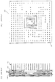
- Figures 1a-1c schematically illustrate the top, side and cross-sectional views of an exemplary PGA package, respectively.
- PGA package 100 includes a large number of pins 110 surrounding a rectangular die-attach area where a semiconductor chip or die 120 is mounted.
- Figure 1b illustrates a cross section through the center of the multi-layered structure of package 100.
- Package 100 includes a number of (for example 9) parallel conductive layers 130, insulated from each other by dielectric layers 140 separating conductive layers 130.
- a plurality of via columns 150 provide for selective interconnection between conductive layers 130, or connections from a conductive layer 130 to a pin 110.
- an input/output signal on the integrated circuit embedded in the semiconductor chip 120 electrically connects to the outside world through a transmission path that includes four segments: (1) an electrically conductive bond wire 160 connecting a chip 120 bonding pad to a corresponding wire bond post on the package, (2) a horizontal conductive strip 170 connecting the bonding post on the package to a selected via column 150, (3) via column 150 vertically connecting conductive strip 170 to a corresponding (4) pin 110 such that when the package is inserted in a socket on a circuit board, chip 120 can transmit and receive signals from other circuits on the board.
- Well controlled transmission line impedances are especially critical in circuits in which the rise or fall time of a signal is short compared to the transit time of the signal down its transmission line. Such circuits are especially susceptible to false switching caused by signal reflection. To reduce signal reflection it is necessary to minimize variations in the impedance of a transmission line through the package as much as possible It is desirable to maintain a uniform impedance of, for example, 50 ohms across the entire transmission path.
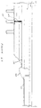
- Figure 2 illustrates a packaging technique according to one embodiment of the present invention, for adjusting the impedance of a via column segment of a transmission path.
- a shield via column 204 is placed in parallel to via column 200 at a precalculated distance D.
- Shield via column 204 connects an upper conductive layer 206 to a lower conductive layer 208, and through strip lines (or conductive planes ) 210 and 212 connects to a via column 214 attached to pin 216.
- Pin 216 connects to ground potential.
- This arrangement of shield via column 204 in parallel with conductor via column 200 emulates a two-wire transmission line.
- the effective impedance of conductor via column 200 can therefore be adjusted by the distance D and/or the via column 200 and 204 diameters. As can be seen from the equation, the effective impedance is reduced as D is made smaller. However, a minimum dimension is set for via center to center spacing for a typical PGA packaging fabrication process.
- a PGA package with a 100 mil pin to pin spacing it is possible to drill vias with, for example, 25 mil center spacing without requiring non-standard tooling.
- the effective impedance of, for example, a three-wire line can be made smaller than the minimum impedance obtainable by a two wire line.
- the multi-layer package of the present invention employs inductance reduction techniques on the ground and power lines in all segments of the transmission path, from the bond wires to the pins. It is desirable to increase the capacitance on power lines so that they behave as low-impedance voltage sources at high frequencies. This will reduce the amount of high frequency noise coupling to other signals through the power supply. Higher capacitance per unit length translates to lower inductance which is also highly desirable on the power and ground lines to reduce ground bounce.
- V p the velocity of propagation of a wave along a transmission line
- V p 1/[ ⁇ (LC)]
- inductance L per unit length and capacitance C per unit length of a transmission line have an inverse relationship. This principle is very helpful in understanding that the desired effect of reduced inductance is an automatic side effect of increased capacitance on power and ground lines.
- the second principle is based on mutual inductance between adjacent wires.
- L1 inductance of wire 1
- L2 inductance of wire 2
- L12 mutant inductance between wires 1 and 2
- a very thin dielectric layer 220 is used for separating power plane 222 from ground plane 224.
- dielectric layers in a typical PGA package fabrication process with, for example, 15 mil thick dielectric layers it is possible to use dielectric layers as thin as, for example, 2 mils.
- a thinner dielectric layer translates into higher capacitance per unit length and lower inductance per unit length. Therefore, using a very thin dielectric between the power planes allows for placing the power supply pins at a corner of the package, farthest away from the die-attach area where the chip is mounted. Because of the lower inductance per unit length, the increased distance will not result in unacceptably high inductance.
- This arrangement has the advantage of making available pins closer to the integrated circuit chip for sensitive electrical signals that require minimum propagation delay in their signal path.
- Figure 3 shows an example of an arrangement for the power supply pins. These pins are arranged in groups of, for example nine, with alternating polarities in a checkerboard fashion and placed in each of the four corners of the package. Given a, for example, 100 mil center spacing between the pins, as a nine-wire line arrangement, there will be cancellation of mutual inductances between positive power supply (VDD) pins 310 and negative power supply (VSS) pins 300 as discussed above. Since each nine-wire checkerboard arrangement will include one pin of one polarity more than the other ( e.g . 5 VSS pins and 4 VDD pins), there will be a slight imbalance in the effective inductances. To compensate for this imbalance, the arrangement is complemented in each of the four corners of the package in an alternating fashion. The reduction in inductance due to this checkerboard arrangement also applies to the corresponding two-wire line vias 320 inside the package.
- VDD positive power supply
- VSS negative power supply
- the above techniques help reduce inductance on power lines and provide for controlled impedance signal lines from the IC bonding pad to the package external pins.
- the multi-layer packaging of the present invention also provides several techniques aimed primarily at reduction of noise for high frequency operation.
- opposite polarity shielding is used in both the vertical and horizontal directions. Such shielding is especially effective for circuits operating with high frequency low-voltage-swing signals.
- Figure 4a illustrates an example of such opposite polarity shielding for a package with nine conductive layers 401 to 409. Four of the conductive layers are assigned to carry active signals and five are connected to high and low power supplies to shield any one signal layer from another.
- Opposite polarity shielding in the vertical direction is obtained by interleaving signal and shield layers in an alternating fashion, such that each signal layer is sandwiched between a high power supply shield layer and a low power supply shield layer. Therefore, in Figure 4a, layers 402, 404, 406 and 408 carry active signals that are sandwiched between shields, layers 401, 405 and 409 connect to the low power supply, and layers 403 and 407 connect to the high power supply.
- Via columns 400 and 410 allow for opposite polarity shielding in the horizontal direction.
- a conductive strip 420 carrying a critical signal is shielded on both sides by conductive strips 430 and 440 running on either side of strip 420.
- Via columns 400 and 410 ( Figure 4a) connect shield strips 430 and 440 to the low power supply and the high power supply, respectively.
- the low power supply and high power supply shield layers may also function as power planes, carrying power signals from the pins in the corners of the package to the bond posts in the center of the package.
- One type of low-voltage-swing circuit operation requires the signals to travel in pairs of true and complement to enable the circuit to distinguish between a logic high and a logic low.
- this type of circuit operation sometimes referred to as fully differential, the opposite polarity shielding described above is very effective.
- another type of low-voltage-swing circuit operation allows sending only one signal (as opposed to a pair of complements) that is compared to a reference voltage Vref to determine its logic state.
- Vref reference voltage
- one line carrying Vref is normally used as the complementary input for all input signals.
- the package of the present invention achieves this by first dividing the signals into groups or bundles, with each bundle sharing its own Vref.
- the signal lines of a bundle are grouped together with half on each side of the Vref line.
- the pins and the vias are arranged such that the distances the signals in any given bundle must travel from the pins to the die are approximately equal. This arrangement maximizes the similarity of the noise environment each signal in a bundle is exposed to.
- shield layers are interleaved between signal layers to provide vertical and horizontal shielding in a similar fashion as illustrated in Figures 4a and 4b. However, this time all shield layers are connected to each other and left floating.
- the floating shield layers allow any noise due to signal switching to be capacitively coupled to all lines adjacent to the shield. That is, since all signal lines and Vref lines are adjacent to a floating shield layer that is connected to all other floating shield layers (vertically as well as horizontally) they are all subject to the same noise coupling and therefore move together. This ensures accurate reading of signal levels when they are compared to the reference voltage by an on-chip differential input buffer. Signal lines having the same lengths ensure equal capacitive coupling between the floating shields and the various signal lines. Shielding in the horizontal direction also helps reduce cross talk between the signals.
- Another shielding technique offered by the packaging of the present invention provides immunity from differential noise on the negative (VSS) and positive (VDD) power supplies.
- the two top layers in the package are assigned to the power supply lines. However, instead of dedicating, for example, the entire top layer to VDD and the entire layer below that to VSS, the layers are arranged such that equal areas of VDD and VSS conductive material are facing at an equal distance the signal line shield areas parallel to them.
- Figures 5a and 5b schematically illustrate the underlying principle of this technique.
- via columns (not shown) connecting the two layers 500 and 510 through dielectric layer 520, are employed to create alternating power supply areas on both layers.
- Figure 5b shows a top view of layer 510 illustrating equal areas of VDD and VSS. This structure provides the shield zones 530 adjacent to these noisy power supply areas with equal and opposite induced voltage. This effectively makes the shields immune to differential VDD/VSS noise.
- circuits operating with different types of signals require different shielding mechanisms.
- an integrated circuit may combine several different types of signals on the same chip.
- the packaging of such integrated circuit chips should therefore, accommodate any combination of or all of the above shielding techniques.
- the package of the present invention provides for effective shielding of various types of signals inside the same package. This is achieved by dividing the package into segregated zones, electrically isolated from each other. Referring back to Figure 4a, all conductive layers are similarly divided into a number of zones corresponding to the number of different signal types.
- Figure 6 shows a top view of an exemplary shield layer 600 divided into three independent zones 601, 602 and 603. Each zone includes a continuous plate of metal to be used as a shield signal. Gaps divide the three zones from each other and allow each shield zone to have its own instantaneous voltage.
- Each zone defines the boundaries of the areas dedicated to one type of signal on all of the signal layers interleaved between the shield layers.
- zones 601, 602 and 603 can be assigned to fully differential low-voltage-swing outputs, quasi differential low-voltage-swing inputs, and CMOS or TTL inputs and outputs, respectively.
- opposite polarity shielding as described in connection with Figures 4a and 4b using the power supply voltages of the low-voltage-swing outputs, is used on all shield and signal layers in areas corresponding to shield zone 601.
- shield zone 602 In areas corresponding to shield zone 602, floating shielding is used on all shield and signal layers, and opposite polarity shielding using the CMOS power supplies (VDD and VSS) is used in shield zone 603 on all shield and signal layers.
- This type of zone shielding is very flexible and provides the most effective shielding for a mixed signal package.
- the present invention offers a packaging apparatus and method of manufacture which is particularly suitable for high frequency, mixed signal integrated circuit devices. While the above is a complete description of the preferred embodiment of the present invention, it is possible to use various alternatives, modifications and equivalents. Therefore, the scope of the present invention should be determined not with reference to the above description but should, instead, be determined with reference to the appended claims, along with their full scope of equivalents.
Landscapes
- Semiconductor Integrated Circuits (AREA)
- Internal Circuitry In Semiconductor Integrated Circuit Devices (AREA)
- Lead Frames For Integrated Circuits (AREA)
- Shielding Devices Or Components To Electric Or Magnetic Fields (AREA)
Priority Applications (1)
| Application Number | Priority Date | Filing Date | Title |
|---|---|---|---|
| EP97121409A EP0834922B1 (de) | 1993-03-24 | 1994-03-23 | Verbesserte Mehrschichtverpackung |
Applications Claiming Priority (2)
| Application Number | Priority Date | Filing Date | Title |
|---|---|---|---|
| US08/036,564 US5338970A (en) | 1993-03-24 | 1993-03-24 | Multi-layered integrated circuit package with improved high frequency performance |
| US36564 | 1998-03-09 |
Related Child Applications (1)
| Application Number | Title | Priority Date | Filing Date |
|---|---|---|---|
| EP97121409A Division EP0834922B1 (de) | 1993-03-24 | 1994-03-23 | Verbesserte Mehrschichtverpackung |
Publications (3)
| Publication Number | Publication Date |
|---|---|
| EP0617466A2 true EP0617466A2 (de) | 1994-09-28 |
| EP0617466A3 EP0617466A3 (de) | 1994-11-30 |
| EP0617466B1 EP0617466B1 (de) | 1998-08-26 |
Family
ID=21889300
Family Applications (2)
| Application Number | Title | Priority Date | Filing Date |
|---|---|---|---|
| EP94104551A Expired - Lifetime EP0617466B1 (de) | 1993-03-24 | 1994-03-23 | Verbesserte Mehrschichtverpackung |
| EP97121409A Expired - Lifetime EP0834922B1 (de) | 1993-03-24 | 1994-03-23 | Verbesserte Mehrschichtverpackung |
Family Applications After (1)
| Application Number | Title | Priority Date | Filing Date |
|---|---|---|---|
| EP97121409A Expired - Lifetime EP0834922B1 (de) | 1993-03-24 | 1994-03-23 | Verbesserte Mehrschichtverpackung |
Country Status (4)
| Country | Link |
|---|---|
| US (2) | US5338970A (de) |
| EP (2) | EP0617466B1 (de) |
| JP (1) | JP3530920B2 (de) |
| DE (2) | DE69431678T2 (de) |
Cited By (4)
| Publication number | Priority date | Publication date | Assignee | Title |
|---|---|---|---|---|
| WO1997015077A1 (de) * | 1995-10-16 | 1997-04-24 | Siemens N.V. | Polymeres höcker-matrix-gehäuse für mikrowellen-schaltungsanordnungen |
| EP1296453A3 (de) * | 2001-09-25 | 2003-06-04 | TDK Corporation | Gehäuse für Integrierte Schaltung |
| US7268420B2 (en) | 2003-12-26 | 2007-09-11 | Elpida Memory, Inc. | Semiconductor device having layered chips |
| US10326116B2 (en) | 2006-08-28 | 2019-06-18 | Sony Corporation | Battery device, electronic apparatus, and battery system |
Families Citing this family (39)
| Publication number | Priority date | Publication date | Assignee | Title |
|---|---|---|---|---|
| US5760452A (en) * | 1991-08-22 | 1998-06-02 | Nec Corporation | Semiconductor memory and method of fabricating the same |
| WO1995010852A1 (en) * | 1993-10-12 | 1995-04-20 | Atmel Corporation | Bonding of leads directly over chip active areas |
| US5543586A (en) * | 1994-03-11 | 1996-08-06 | The Panda Project | Apparatus having inner layers supporting surface-mount components |
| FR2747235B1 (fr) * | 1996-04-03 | 1998-07-10 | Bull Sa | Boitier de circuit integre |
| AU5238898A (en) * | 1996-11-08 | 1998-05-29 | W.L. Gore & Associates, Inc. | Method for reducing via inductance in an electronic assembly and device |
| US6054758A (en) * | 1996-12-18 | 2000-04-25 | Texas Instruments Incorporated | Differential pair geometry for integrated circuit chip packages |
| SE511377C2 (sv) * | 1996-12-19 | 1999-09-20 | Ericsson Telefon Ab L M | Viaanordning |
| US5886597A (en) * | 1997-03-28 | 1999-03-23 | Virginia Tech Intellectual Properties, Inc. | Circuit structure including RF/wideband resonant vias |
| US7321485B2 (en) | 1997-04-08 | 2008-01-22 | X2Y Attenuators, Llc | Arrangement for energy conditioning |
| US9054094B2 (en) | 1997-04-08 | 2015-06-09 | X2Y Attenuators, Llc | Energy conditioning circuit arrangement for integrated circuit |
| US7336468B2 (en) | 1997-04-08 | 2008-02-26 | X2Y Attenuators, Llc | Arrangement for energy conditioning |
| US5874778A (en) * | 1997-06-11 | 1999-02-23 | International Business Machines Corporation | Embedded power and ground plane structure |
| US5977850A (en) * | 1997-11-05 | 1999-11-02 | Motorola, Inc. | Multilayer ceramic package with center ground via for size reduction |
| US6242767B1 (en) * | 1997-11-10 | 2001-06-05 | Lightspeed Semiconductor Corp. | Asic routing architecture |
| US5990752A (en) * | 1998-05-14 | 1999-11-23 | Cts Corporation | Method for mechanically tuning a voltage controlled oscillator |
| US6434726B1 (en) | 1999-06-29 | 2002-08-13 | Lucent Technologies Inc. | System and method of transmission using coplanar bond wires |
| US6246252B1 (en) * | 1999-07-30 | 2001-06-12 | Sun Microsystems, Inc. | Efficient debug package design |
| US6510545B1 (en) * | 2000-01-19 | 2003-01-21 | Sun Microsystems, Inc. | Automated shielding algorithm for dynamic circuits |
| DE10002377A1 (de) | 2000-01-20 | 2001-08-02 | Infineon Technologies Ag | Spule und Spulensystem zur Integration in eine mikroelektronische Schaltung sowie mikroelektronische Schaltung |
| US6613611B1 (en) | 2000-12-22 | 2003-09-02 | Lightspeed Semiconductor Corporation | ASIC routing architecture with variable number of custom masks |
| US6627822B2 (en) * | 2001-06-27 | 2003-09-30 | Intel Corporation | Electronic assembly with separate power and signal connections |
| AU2002360943A1 (en) | 2001-11-13 | 2003-05-26 | International Business Machines Corporation | Electronic device carrier adapted for transmitting high frequency signals |
| US6885043B2 (en) * | 2002-01-18 | 2005-04-26 | Lightspeed Semiconductor Corporation | ASIC routing architecture |
| JP4005451B2 (ja) * | 2002-08-29 | 2007-11-07 | 富士通株式会社 | 多層基板及び半導体装置 |
| US7038319B2 (en) * | 2003-08-20 | 2006-05-02 | International Business Machines Corporation | Apparatus and method to reduce signal cross-talk |
| US7501586B2 (en) * | 2004-10-29 | 2009-03-10 | Intel Corporation | Apparatus and method for improving printed circuit board signal layer transitions |
| JP2008537843A (ja) | 2005-03-01 | 2008-09-25 | エックストゥーワイ アテニュエイターズ,エルエルシー | 内部で重なり合った調整器 |
| CA2614982A1 (en) * | 2005-07-14 | 2007-01-18 | Tir Technology Lp | Power board and plug-in lighting module |
| US7880161B2 (en) * | 2007-02-16 | 2011-02-01 | Mears Technologies, Inc. | Multiple-wavelength opto-electronic device including a superlattice |
| JP5142749B2 (ja) | 2008-02-14 | 2013-02-13 | キヤノン株式会社 | 撮像装置、撮像装置の制御方法及び撮像システム |
| US8350379B2 (en) * | 2008-09-09 | 2013-01-08 | Lsi Corporation | Package with power and ground through via |
| US9107325B1 (en) | 2009-08-10 | 2015-08-11 | The Boeing Company | Systems and methods of coupling sensors to a structure |
| WO2011096164A1 (ja) * | 2010-02-03 | 2011-08-11 | 本田技研工業株式会社 | 半導体装置 |
| US8927879B2 (en) * | 2010-11-22 | 2015-01-06 | International Business Machines Corporation | Crosstalk reduction between signal layers in a multilayered package by variable-width mesh plane structures |
| US9362606B2 (en) | 2013-08-23 | 2016-06-07 | International Business Machines Corporation | On-chip vertical three dimensional microstrip line with characteristic impedance tuning technique and design structures |
| US9634667B2 (en) | 2014-08-29 | 2017-04-25 | Cypress Semiconductor Corporation | Integrated circuit device with programmable analog subsystem |
| US9473144B1 (en) * | 2014-11-25 | 2016-10-18 | Cypress Semiconductor Corporation | Integrated circuit device with programmable analog subsystem |
| US11309246B2 (en) | 2020-02-05 | 2022-04-19 | Apple Inc. | High density 3D interconnect configuration |
| US20260031717A1 (en) * | 2022-07-18 | 2026-01-29 | Magna powertrain gmbh & co kg | Multi-phase power converter circuit layout to minimize drive loop and power loop inductances |
Family Cites Families (19)
| Publication number | Priority date | Publication date | Assignee | Title |
|---|---|---|---|---|
| JPS547196B2 (de) * | 1971-08-26 | 1979-04-04 | ||
| US4551746A (en) * | 1982-10-05 | 1985-11-05 | Mayo Foundation | Leadless chip carrier apparatus providing an improved transmission line environment and improved heat dissipation |
| US4513355A (en) * | 1983-06-15 | 1985-04-23 | Motorola, Inc. | Metallization and bonding means and method for VLSI packages |
| KR900001273B1 (ko) * | 1983-12-23 | 1990-03-05 | 후지쑤 가부시끼가이샤 | 반도체 집적회로 장치 |
| JPS60134440A (ja) * | 1983-12-23 | 1985-07-17 | Hitachi Ltd | 半導体集積回路装置 |
| CA1246755A (en) * | 1985-03-30 | 1988-12-13 | Akira Miyauchi | Semiconductor device |
| JPS61239649A (ja) * | 1985-04-13 | 1986-10-24 | Fujitsu Ltd | 高速集積回路パツケ−ジ |
| JPH0812887B2 (ja) * | 1985-04-13 | 1996-02-07 | 富士通株式会社 | 高速集積回路パツケ−ジ |
| CA1320006C (en) * | 1986-06-02 | 1993-07-06 | Norio Hidaka | Package for integrated circuit |
| US4811116A (en) * | 1986-10-10 | 1989-03-07 | Eastman Kodak Company | Video recorder using extended tape tracks to record compressed chrominance |
| JPH0793392B2 (ja) * | 1986-10-25 | 1995-10-09 | 新光電気工業株式会社 | 超高周波素子用パツケ−ジ |
| US4811082A (en) * | 1986-11-12 | 1989-03-07 | International Business Machines Corporation | High performance integrated circuit packaging structure |
| JPH088321B2 (ja) * | 1987-01-19 | 1996-01-29 | 住友電気工業株式会社 | 集積回路パツケ−ジ |
| EP0331289A3 (de) * | 1988-02-26 | 1991-04-03 | Hitachi, Ltd. | Halbleiteranordnung mit Impedanz-Anpassungsmitteln |
| JPH0716100B2 (ja) * | 1990-01-10 | 1995-02-22 | インターナショナル・ビジネス・マシーンズ・コーポレーション | 多層配線モジュール |
| EP0459179B1 (de) * | 1990-05-28 | 1995-04-05 | Siemens Aktiengesellschaft | IC-Gehäuse, bestehend aus drei beschichteten dielektrischen Platten |
| JP2978533B2 (ja) * | 1990-06-15 | 1999-11-15 | 株式会社日立製作所 | 半導体集積回路装置 |
| JPH04256203A (ja) * | 1991-02-07 | 1992-09-10 | Mitsubishi Electric Corp | マイクロ波帯ic用パッケージ |
| JPH05160292A (ja) * | 1991-06-06 | 1993-06-25 | Toshiba Corp | 多層パッケージ |
-
1993
- 1993-03-24 US US08/036,564 patent/US5338970A/en not_active Expired - Lifetime
-
1994
- 1994-03-23 DE DE69431678T patent/DE69431678T2/de not_active Expired - Fee Related
- 1994-03-23 DE DE69412678T patent/DE69412678T2/de not_active Expired - Fee Related
- 1994-03-23 EP EP94104551A patent/EP0617466B1/de not_active Expired - Lifetime
- 1994-03-23 EP EP97121409A patent/EP0834922B1/de not_active Expired - Lifetime
- 1994-03-24 JP JP05380294A patent/JP3530920B2/ja not_active Expired - Fee Related
- 1994-04-13 US US08/226,920 patent/US5499445A/en not_active Expired - Lifetime
Cited By (9)
| Publication number | Priority date | Publication date | Assignee | Title |
|---|---|---|---|---|
| WO1997015077A1 (de) * | 1995-10-16 | 1997-04-24 | Siemens N.V. | Polymeres höcker-matrix-gehäuse für mikrowellen-schaltungsanordnungen |
| US6130478A (en) * | 1995-10-16 | 2000-10-10 | Siemens N.V. | Polymer stud grid array for microwave circuit arrangements |
| KR100421301B1 (ko) * | 1995-10-16 | 2004-09-18 | 인터유니베르지테르 마이크로-엘렉트로니카 센트룸 파우체트베 | 마이크로파회로시스템을위한폴리머스터드그리드어레이 |
| EP1296453A3 (de) * | 2001-09-25 | 2003-06-04 | TDK Corporation | Gehäuse für Integrierte Schaltung |
| US7151310B2 (en) | 2001-09-25 | 2006-12-19 | Tdk Corporation | Package substrate, integrated circuit apparatus, substrate unit, surface acoustic wave apparatus, and circuit device |
| US7304377B2 (en) | 2001-09-25 | 2007-12-04 | Tdk Corporation | Package substrate, integrated circuit apparatus, substrate unit, surface acoustic wave apparatus, and circuit device |
| US7268420B2 (en) | 2003-12-26 | 2007-09-11 | Elpida Memory, Inc. | Semiconductor device having layered chips |
| US7576421B2 (en) | 2003-12-26 | 2009-08-18 | Elpida Memory, Inc. | Semiconductor device having a multi-layered semiconductor substrate |
| US10326116B2 (en) | 2006-08-28 | 2019-06-18 | Sony Corporation | Battery device, electronic apparatus, and battery system |
Also Published As
| Publication number | Publication date |
|---|---|
| EP0617466A3 (de) | 1994-11-30 |
| DE69431678T2 (de) | 2003-09-18 |
| JP3530920B2 (ja) | 2004-05-24 |
| US5338970A (en) | 1994-08-16 |
| EP0834922B1 (de) | 2002-11-06 |
| DE69431678D1 (de) | 2002-12-12 |
| EP0617466B1 (de) | 1998-08-26 |
| EP0834922A3 (de) | 1998-04-15 |
| DE69412678D1 (de) | 1998-10-01 |
| EP0834922A2 (de) | 1998-04-08 |
| JPH07169880A (ja) | 1995-07-04 |
| US5499445A (en) | 1996-03-19 |
| DE69412678T2 (de) | 1999-04-01 |
Similar Documents
| Publication | Publication Date | Title |
|---|---|---|
| US5499445A (en) | Method of making a multi-layer to package | |
| US4686492A (en) | Impedance match connection using multiple layers of bond wires | |
| JP4373531B2 (ja) | 差動平衡信号伝送基板 | |
| USRE43720E1 (en) | Integrated circuit device having stacked dies and impedance balanced transmission lines | |
| US5304743A (en) | Multilayer IC semiconductor package | |
| US4210885A (en) | Thin film lossy line for preventing reflections in microcircuit chip package interconnections | |
| JP3480291B2 (ja) | 半導体装置及び電子装置 | |
| JPH073830B2 (ja) | 集積回路の試験装置 | |
| US7298040B2 (en) | Wire bonding method and apparatus for integrated circuit | |
| US20080035362A1 (en) | Method and structure for controlled impedance wire bonds using co-dispensing of dielectric spacers | |
| KR100271860B1 (ko) | 메모리모듈 및 ic카드 | |
| JPH0653351A (ja) | 多層配線を有する電子パッケージ基板及び方法 | |
| KR19980064367A (ko) | 집적 회로 칩 패키지용 차동 쌍 구성 | |
| CN103687274A (zh) | 多层式印刷电路板 | |
| JP4659087B2 (ja) | 差動平衡信号伝送基板 | |
| US6563208B2 (en) | Semiconductor package with conductor impedance selected during assembly | |
| US7466021B2 (en) | Memory packages having stair step interconnection layers | |
| JP2003134177A (ja) | デジタル信号伝送回路の設計方法 | |
| EP0624055B1 (de) | Energiezuführungsstruktur für ein Multichip | |
| US5334802A (en) | Method and configuration for reducing electrical noise in integrated circuit devices | |
| EP0410164A2 (de) | Orthogonale Linienstruktur vom "Floating"-Typ für X-Y-Leiterfläche | |
| JPH0691179B2 (ja) | 半導体集積回路装置 |
Legal Events
| Date | Code | Title | Description |
|---|---|---|---|
| PUAI | Public reference made under article 153(3) epc to a published international application that has entered the european phase |
Free format text: ORIGINAL CODE: 0009012 |
|
| AK | Designated contracting states |
Kind code of ref document: A2 Designated state(s): DE FR GB IT NL |
|
| PUAL | Search report despatched |
Free format text: ORIGINAL CODE: 0009013 |
|
| AK | Designated contracting states |
Kind code of ref document: A3 Designated state(s): DE FR GB IT NL |
|
| 17P | Request for examination filed |
Effective date: 19950510 |
|
| 17Q | First examination report despatched |
Effective date: 19960621 |
|
| GRAG | Despatch of communication of intention to grant |
Free format text: ORIGINAL CODE: EPIDOS AGRA |
|
| GRAG | Despatch of communication of intention to grant |
Free format text: ORIGINAL CODE: EPIDOS AGRA |
|
| GRAG | Despatch of communication of intention to grant |
Free format text: ORIGINAL CODE: EPIDOS AGRA |
|
| GRAH | Despatch of communication of intention to grant a patent |
Free format text: ORIGINAL CODE: EPIDOS IGRA |
|
| GRAH | Despatch of communication of intention to grant a patent |
Free format text: ORIGINAL CODE: EPIDOS IGRA |
|
| GRAA | (expected) grant |
Free format text: ORIGINAL CODE: 0009210 |
|
| AK | Designated contracting states |
Kind code of ref document: B1 Designated state(s): DE FR GB IT NL |
|
| REF | Corresponds to: |
Ref document number: 69412678 Country of ref document: DE Date of ref document: 19981001 |
|
| ET | Fr: translation filed | ||
| PLBE | No opposition filed within time limit |
Free format text: ORIGINAL CODE: 0009261 |
|
| STAA | Information on the status of an ep patent application or granted ep patent |
Free format text: STATUS: NO OPPOSITION FILED WITHIN TIME LIMIT |
|
| 26N | No opposition filed | ||
| REG | Reference to a national code |
Ref country code: GB Ref legal event code: IF02 |
|
| NLS | Nl: assignments of ep-patents |
Owner name: INTERGRAPH HARDWARE TECHNOLOGIES COMPANY |
|
| REG | Reference to a national code |
Ref country code: GB Ref legal event code: 732E |
|
| REG | Reference to a national code |
Ref country code: FR Ref legal event code: TP |
|
| PGFP | Annual fee paid to national office [announced via postgrant information from national office to epo] |
Ref country code: NL Payment date: 20090310 Year of fee payment: 16 |
|
| PGFP | Annual fee paid to national office [announced via postgrant information from national office to epo] |
Ref country code: GB Payment date: 20090206 Year of fee payment: 16 |
|
| PGFP | Annual fee paid to national office [announced via postgrant information from national office to epo] |
Ref country code: IT Payment date: 20090318 Year of fee payment: 16 Ref country code: DE Payment date: 20090331 Year of fee payment: 16 |
|
| PGFP | Annual fee paid to national office [announced via postgrant information from national office to epo] |
Ref country code: FR Payment date: 20090306 Year of fee payment: 16 |
|
| REG | Reference to a national code |
Ref country code: NL Ref legal event code: V1 Effective date: 20101001 |
|
| GBPC | Gb: european patent ceased through non-payment of renewal fee |
Effective date: 20100323 |
|
| REG | Reference to a national code |
Ref country code: FR Ref legal event code: ST Effective date: 20101130 |
|
| PG25 | Lapsed in a contracting state [announced via postgrant information from national office to epo] |
Ref country code: NL Free format text: LAPSE BECAUSE OF NON-PAYMENT OF DUE FEES Effective date: 20101001 Ref country code: FR Free format text: LAPSE BECAUSE OF NON-PAYMENT OF DUE FEES Effective date: 20100331 |
|
| PG25 | Lapsed in a contracting state [announced via postgrant information from national office to epo] |
Ref country code: DE Free format text: LAPSE BECAUSE OF NON-PAYMENT OF DUE FEES Effective date: 20101001 |
|
| PG25 | Lapsed in a contracting state [announced via postgrant information from national office to epo] |
Ref country code: GB Free format text: LAPSE BECAUSE OF NON-PAYMENT OF DUE FEES Effective date: 20100323 Ref country code: IT Free format text: LAPSE BECAUSE OF NON-PAYMENT OF DUE FEES Effective date: 20100323 |