EP0617470A2 - Licht emittierende Halbleitervorrichtung und Verfahren zu ihrer Herstellung - Google Patents
Licht emittierende Halbleitervorrichtung und Verfahren zu ihrer Herstellung Download PDFInfo
- Publication number
- EP0617470A2 EP0617470A2 EP94104630A EP94104630A EP0617470A2 EP 0617470 A2 EP0617470 A2 EP 0617470A2 EP 94104630 A EP94104630 A EP 94104630A EP 94104630 A EP94104630 A EP 94104630A EP 0617470 A2 EP0617470 A2 EP 0617470A2
- Authority
- EP
- European Patent Office
- Prior art keywords
- light emitting
- nitrogen
- emitting device
- doped
- compound semiconductor
- Prior art date
- Legal status (The legal status is an assumption and is not a legal conclusion. Google has not performed a legal analysis and makes no representation as to the accuracy of the status listed.)
- Ceased
Links
Images


Classifications
-
- H—ELECTRICITY
- H10—SEMICONDUCTOR DEVICES; ELECTRIC SOLID-STATE DEVICES NOT OTHERWISE PROVIDED FOR
- H10H—INORGANIC LIGHT-EMITTING SEMICONDUCTOR DEVICES HAVING POTENTIAL BARRIERS
- H10H20/00—Individual inorganic light-emitting semiconductor devices having potential barriers, e.g. light-emitting diodes [LED]
- H10H20/80—Constructional details
- H10H20/81—Bodies
- H10H20/822—Materials of the light-emitting regions
- H10H20/824—Materials of the light-emitting regions comprising only Group III-V materials, e.g. GaP
-
- H—ELECTRICITY
- H10—SEMICONDUCTOR DEVICES; ELECTRIC SOLID-STATE DEVICES NOT OTHERWISE PROVIDED FOR
- H10H—INORGANIC LIGHT-EMITTING SEMICONDUCTOR DEVICES HAVING POTENTIAL BARRIERS
- H10H20/00—Individual inorganic light-emitting semiconductor devices having potential barriers, e.g. light-emitting diodes [LED]
- H10H20/01—Manufacture or treatment
- H10H20/011—Manufacture or treatment of bodies, e.g. forming semiconductor layers
- H10H20/013—Manufacture or treatment of bodies, e.g. forming semiconductor layers having light-emitting regions comprising only Group III-V materials
-
- H—ELECTRICITY
- H10—SEMICONDUCTOR DEVICES; ELECTRIC SOLID-STATE DEVICES NOT OTHERWISE PROVIDED FOR
- H10H—INORGANIC LIGHT-EMITTING SEMICONDUCTOR DEVICES HAVING POTENTIAL BARRIERS
- H10H20/00—Individual inorganic light-emitting semiconductor devices having potential barriers, e.g. light-emitting diodes [LED]
- H10H20/80—Constructional details
- H10H20/81—Bodies
- H10H20/822—Materials of the light-emitting regions
- H10H20/824—Materials of the light-emitting regions comprising only Group III-V materials, e.g. GaP
- H10H20/8242—Materials of the light-emitting regions comprising only Group III-V materials, e.g. GaP characterised by the dopants
-
- Y—GENERAL TAGGING OF NEW TECHNOLOGICAL DEVELOPMENTS; GENERAL TAGGING OF CROSS-SECTIONAL TECHNOLOGIES SPANNING OVER SEVERAL SECTIONS OF THE IPC; TECHNICAL SUBJECTS COVERED BY FORMER USPC CROSS-REFERENCE ART COLLECTIONS [XRACs] AND DIGESTS
- Y10—TECHNICAL SUBJECTS COVERED BY FORMER USPC
- Y10S—TECHNICAL SUBJECTS COVERED BY FORMER USPC CROSS-REFERENCE ART COLLECTIONS [XRACs] AND DIGESTS
- Y10S438/00—Semiconductor device manufacturing: process
- Y10S438/914—Doping
- Y10S438/925—Fluid growth doping control, e.g. delta doping
Definitions
- This invention relates to a semiconductor light emitting device and methods of manufacturing it, and more precisely to a semiconductor light emitting device which gives a pure green light emission at a higt brightness and methods of manufacturing it.
- Semiconductor light emitting devices such as light emitting diodes, are obtained by growing a plurality of semiconductor layers on the front surface of a semiconductor substrate to fabricate a multi-layer semiconductor structure with a p-n junction(s) and then cutting it into an element(s).
- green light emitting semiconductor devices are obtained by forming one or more layers of both n-type and p-type GaP one after another on an n-type GaP single crystal substrate and cutting it into elements for practical use.
- GaP has an indirect transition-type band structure
- the light emission efficiency is not sufficient if the p-n junction(s) is just formed, resulting in a light emitting device with a very low brightness.
- the incorporation of isoelectronic traps which function as light emitting centers is performed as an effective means to improve the light emitting efficiency.
- nitrogen (N) is doped to the GaP layer(s) near the p-n junction to substitute P sites in order to improve the light emitting efficiency.
- a GaP-type light emitting device thus doped with nitrogen emits a yellowish-green light with a peak wavelength of approximately 567 nm.
- GaP semiconductor light emitting devices has a long history, and the light emitting efficiency of the GaP semiconductor light emitting devices has been improved to the limit of the material property. However, it has been a problem that a sufficient light emitting efficiency could not be achieved because, as mentioned above, GaP essentially had an indirect transition-type band structure. Although the nitrogen doped GaP-type light emitting devices improved the light emitting efficiency, since the energy level of nitrogen was formed within the GaP band gap, it has been a problem that the light emitting wavelength became longer and the color changed to yellowish-green, and thus a pure green light could not be obtained.
- the object of this invention is to provide a semiconductor light emitting device which gives a pure green light emission with a high-brightness, and methods of manufacturing it.
- an epitaxial layer(s) of compound semiconductor alloy doped with nitrogen and represented by the formula (Al x Ga 1-x ) y In 1-y P ( 0 ⁇ x ⁇ 1, 0 ⁇ y ⁇ 1 ) is formed on a compound semiconductor single crystal substrate composed of an element(s) from Group III and an element(s) from Group V in the periodic table by means of the metalorganic vapor phase epitaxy method (MOVPE method), while controlling the amount of the organic aluminum compound introduced.
- Said organic aluminum compound is, for example, trimethyl aluminum (TMAl).
- said nitrogen-doped epitaxial layer is an active layer composed of said compound semiconductor alloy which has a band gap of 2.30 eV or larger and also has an alloy composition of an indirect transition area or similar to it, then this layer can be used as an active layer which emits a pure green light with a high-brightnes.
- the compound semiconductor alloy represented by the formula (Al x Ga 1-x ) y In 1-y P ( 0 ⁇ x ⁇ 1, 0 ⁇ y ⁇ 1 ), can be efficiently doped with nitrogen by means of the MOVPE method if the amount of the organic aluminum compound introduced is controlled.
- a pure green light emission whose wavelength is 555 nm can be obtained by forming an active layer formed by nitrogen doping to (Al x Ga 1-x ) y In 1-y P which has a band gap of 2.30 eV or larger and also has an alloy composition of an indirect transition area or similar to it.
- Figure 1 is a schematic cross section of a semiconductor light emitting device of one example of this invention.
- Figure 2 is an illustration which shows an example of the growth apparatus used in the MOVPE method.
- Figure 3 is a figure which shows the relationship between the NH3 concentration ratio in the reaction gas during the active layer growth and the nitrogen concentration in the active layer.
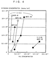
- Figure 4 is a figure which shows the nitrogen concentrations in the active layer with various growth conditions of the active layer.
- the MOVPE method is adopted.
- the material source for Al Ga and P, trimethyl aluminum (TMAl), trimethyl gallium (TMGa) and phosphine (PH3), are used respectively.
- TMAl trimethyl aluminum
- TMGa trimethyl gallium
- PH3 phosphine
- NH3 is used because the highest purity can be obtained.
- H2Se hydrogen selenide
- DMZn dimethyl zinc
- Figure 1 is a schematic cross section of a semiconductor light emitting device of one example of this invention.
- This light emitting device is fabricated by growing a n-type AlGaP layer 4, a N-doped n-type Al GaP layer 3, a N-doped p-type AlGaP layer 2 and a p-type AlGaP layer 1, in this order, on a n-type GaP substrate 5 by means of the MOVPE method.
- a growth apparatus with the configuration shown in figure 2, for example, is used.
- a mixed gas of various vapors of metalorganic compounds of Group III elements, a hydride gas of Group V element and ammonia are fed into a process tube 20, with partial pressures and flow rates adjusted according to the composition of the growing layer, and the desired layers are formed one after another on the n-type GaP substrate 5 which is placed in the process tube 20.
- the n-type AlGaP layer 4 is formed on the n-type GaP substrate 5 which has a diameter of 50 mm and a crystal orientation of (100), by supplying, mixed source gases prepared in such a way that the supply ratio of the Group V element(s) and the Group III element(s) (V/III ratio) is 100, under the following growth conditions: a growth temperature of 850°C and a growth rate of approximately 4 micrometers/hour. Then, NH3 is fed under these growth conditions to form the N-doped n-type AlGaP layer 3.
- the N-doped p-type AlGaP layer 2, and finally the p-type AlGaP layer 1 are formed.
- a p-type GaP layer may be formed on top of these layers to prevent oxidation. The structure shown in figure 1 is thus obtained and cut into elements to obtain light emitting devices such as light emitting diodes.
- the nitrogen doping characteristics are investigated.
- the concentration ratio of NH3 in the mixed gases is varied while the other growth conditions are held constant to determine the changes of nitrogen doping amount in the AlGaP layer.
- Figure 3 shows the relationship between the NH3 concentration ratio and the nitrogen concentration in the AlGaP layer. As shown in figure 3, they are highly correlated. This indicates that the nitrogen doping amount in the AlGaP layer can be controlled by adjusting the NH3 concentration ratio. It is also found that the single crystal state can be maintained while doping the nitrogen, when the NH3 concentration ratio is equal to or lower than the critical concentration ratio corresponding to each growth condition. When the concentration is higher than the critical concentration ratio, AlN with a wultzite structure is formed and the epitaxial layer becomes polycrystals.
- Figure 4 indicates that the larger AlP molar ratio x of the alloy Al x Ga 1-x P tends to have higher nitrogen concentration in the AlGaP layer when the NH3 concentration is the same, resulting in more efficient nitrogen doping, if other conditions are identical.
- NH3 is used as a N source, we believe an adduct (TMAl : NH3) is formed between NH3 and TMAl and the chemical bonding between Al and N plays an important role when N is doped in AlGaP. In fact, it is extremely hard to dope nitrogen in GaP when the GaP is being formed by the MOVPE method without the presence of TMAl.
- Figure 4 also indicates shows that a higher growth temperature and a lower V/III ratio help efficient nitrogen doping.
- Table 2 compares the light emitting device of this example which has a nitrogen-doped AlGaP layer(s) with those of conventional light emitting devices about some characteristics.
- Table 2 LIGHT EMITTING DEVICE LIGHT EMISSION WAVELENGTH (nm)
- This example provides a pure green light emission wavelength 555 nm, which is the same as that of the GaP light emitting device with no nitrogen doping.
- the external quantum efficiency and the visual efficiency which are indicators of brightness, have improved drastically over the GaP light emitting device with no nitrogen doping, and are comparable to the values of the nitrogen-doped GaP light emitting device.
- the case of growing Al x Ga 1-x P on a GaP substrate is chosen as an example.
- lattice-matched (Al x Ga 1-x ) y In 1-y P on the GaAs substrate use NH3 as the nitrogen source, other nitrogen compounds, such as trimethyl amine or dimethyl hydrazine can also be used.
- the MOVPE method is used as the epitaxial growth method, but we believe other methods such as the CBE method (chemical beam epitaxial method) can also be used.
- TMAl trimethyl aluminum
- TMGa trimethyl gallium
- PH3 phosphine
- H2Se hydrogen selenide
- DMZn dimethyl zinc
- this invention makes it possible to obtain a semiconductor light emitting device which gives a high-brightness pure green light emission.
Landscapes
- Led Devices (AREA)
Applications Claiming Priority (2)
| Application Number | Priority Date | Filing Date | Title |
|---|---|---|---|
| JP90736/93 | 1993-03-25 | ||
| JP9073693A JP2773597B2 (ja) | 1993-03-25 | 1993-03-25 | 半導体発光装置及びその製造方法 |
Publications (2)
| Publication Number | Publication Date |
|---|---|
| EP0617470A2 true EP0617470A2 (de) | 1994-09-28 |
| EP0617470A3 EP0617470A3 (de) | 1995-03-01 |
Family
ID=14006867
Family Applications (1)
| Application Number | Title | Priority Date | Filing Date |
|---|---|---|---|
| EP94104630A Ceased EP0617470A3 (de) | 1993-03-25 | 1994-03-23 | Licht emittierende Halbleitervorrichtung und Verfahren zu ihrer Herstellung. |
Country Status (3)
| Country | Link |
|---|---|
| US (2) | US5442201A (de) |
| EP (1) | EP0617470A3 (de) |
| JP (1) | JP2773597B2 (de) |
Cited By (3)
| Publication number | Priority date | Publication date | Assignee | Title |
|---|---|---|---|---|
| US6081540A (en) * | 1996-12-20 | 2000-06-27 | Sharp Kabushiki Kaisha | Semiconductor light emitting device with high light emission efficiency |
| WO2000055398A1 (fr) | 1999-03-18 | 2000-09-21 | Sharp Kabushiki Kaisha | Tirage de cristaux, formation d'une structure fine de semiconducteur, dispositif semiconducteur et systeme |
| WO2011163186A1 (en) * | 2010-06-23 | 2011-12-29 | Massachusetts Institute Of Technology | Engineering emission wavelengths in laser and light emitting devices |
Families Citing this family (9)
| Publication number | Priority date | Publication date | Assignee | Title |
|---|---|---|---|---|
| US5786233A (en) * | 1996-02-20 | 1998-07-28 | U.S. Philips Corporation | Photo-assisted annealing process for activation of acceptors in semiconductor compound layers |
| JP4097232B2 (ja) | 1996-09-05 | 2008-06-11 | 株式会社リコー | 半導体レーザ素子 |
| US6072196A (en) * | 1996-09-05 | 2000-06-06 | Ricoh Company, Ltd. | semiconductor light emitting devices |
| JP3854693B2 (ja) * | 1996-09-30 | 2006-12-06 | キヤノン株式会社 | 半導体レーザの製造方法 |
| US5986288A (en) * | 1997-02-27 | 1999-11-16 | Showa Denko K.K. | Epitaxial wafer for a light-emitting diode and a light-emitting diode |
| JP3698402B2 (ja) * | 1998-11-30 | 2005-09-21 | シャープ株式会社 | 発光ダイオード |
| JP3791672B2 (ja) * | 2001-04-27 | 2006-06-28 | 信越半導体株式会社 | 発光素子及びその製造方法 |
| RU2007117152A (ru) * | 2004-10-08 | 2008-11-20 | Дзе Риджентс Оф Дзе Юниверсити Оф Калифорния (Us) | Высокоэффективные светоизлучающие диоды |
| CN104412396B (zh) | 2012-07-05 | 2021-11-09 | 亮锐控股有限公司 | 具有含氮和磷的发光层的发光二极管 |
Family Cites Families (16)
| Publication number | Priority date | Publication date | Assignee | Title |
|---|---|---|---|---|
| US4001056A (en) * | 1972-12-08 | 1977-01-04 | Monsanto Company | Epitaxial deposition of iii-v compounds containing isoelectronic impurities |
| US4101920A (en) * | 1975-01-29 | 1978-07-18 | Sony Corporation | Green light emitting diode |
| FR2508244A1 (fr) * | 1981-06-19 | 1982-12-24 | Thomson Csf | Laser a semi-conducteur a courte longueur d'onde |
| JPS584987A (ja) * | 1981-07-02 | 1983-01-12 | Stanley Electric Co Ltd | 半導体発光装置およびその製造方法 |
| JPS584988A (ja) * | 1981-07-02 | 1983-01-12 | Stanley Electric Co Ltd | 半導体発光装置 |
| JPS586184A (ja) * | 1981-07-02 | 1983-01-13 | Stanley Electric Co Ltd | 半導体発光装置 |
| JPS5846685A (ja) * | 1981-09-16 | 1983-03-18 | Fujitsu Ltd | 高輝度黄緑色発光ダイオ−ド |
| JPS5861684A (ja) * | 1981-10-07 | 1983-04-12 | Matsushita Electric Ind Co Ltd | 発光半導体装置 |
| JPS63128775A (ja) * | 1986-11-19 | 1988-06-01 | Sumitomo Metal Ind Ltd | 発光素子 |
| JPS63205921A (ja) * | 1987-02-23 | 1988-08-25 | Toshiba Corp | 光半導体素子の製造方法 |
| US5115286A (en) * | 1988-08-26 | 1992-05-19 | Hewlett-Packard Company | Electro-optical device with inverted transparent substrate and method for making same |
| JPH0712094B2 (ja) * | 1988-10-19 | 1995-02-08 | 信越半導体株式会社 | 発光半導体素子用エピタキシャルウェーハの製造方法 |
| US5008718A (en) * | 1989-12-18 | 1991-04-16 | Fletcher Robert M | Light-emitting diode with an electrically conductive window |
| US5173751A (en) * | 1991-01-21 | 1992-12-22 | Pioneer Electronic Corporation | Semiconductor light emitting device |
| JPH04278522A (ja) * | 1991-03-06 | 1992-10-05 | Mitsubishi Cable Ind Ltd | SiドープGaInPキャップ層を有する半導体材料 |
| US5164798A (en) * | 1991-07-05 | 1992-11-17 | Hewlett-Packard Company | Diffusion control of P-N junction location in multilayer heterostructure light emitting devices |
-
1993
- 1993-03-25 JP JP9073693A patent/JP2773597B2/ja not_active Expired - Lifetime
-
1994
- 1994-03-23 US US08/216,278 patent/US5442201A/en not_active Expired - Fee Related
- 1994-03-23 EP EP94104630A patent/EP0617470A3/de not_active Ceased
-
1995
- 1995-03-10 US US08/402,487 patent/US5597761A/en not_active Expired - Fee Related
Cited By (5)
| Publication number | Priority date | Publication date | Assignee | Title |
|---|---|---|---|---|
| US6081540A (en) * | 1996-12-20 | 2000-06-27 | Sharp Kabushiki Kaisha | Semiconductor light emitting device with high light emission efficiency |
| DE19756856B4 (de) * | 1996-12-20 | 2008-06-26 | Sharp K.K. | Halbleiterlichtemissionsvorrichtung mit hoher Lichtemissionswirksamkeit |
| WO2000055398A1 (fr) | 1999-03-18 | 2000-09-21 | Sharp Kabushiki Kaisha | Tirage de cristaux, formation d'une structure fine de semiconducteur, dispositif semiconducteur et systeme |
| WO2011163186A1 (en) * | 2010-06-23 | 2011-12-29 | Massachusetts Institute Of Technology | Engineering emission wavelengths in laser and light emitting devices |
| US8242480B2 (en) | 2010-06-23 | 2012-08-14 | Massachusetts Institute Of Technology | Engineering emission wavelengths in laser and light emitting devices |
Also Published As
| Publication number | Publication date |
|---|---|
| EP0617470A3 (de) | 1995-03-01 |
| JPH06283760A (ja) | 1994-10-07 |
| US5597761A (en) | 1997-01-28 |
| US5442201A (en) | 1995-08-15 |
| JP2773597B2 (ja) | 1998-07-09 |
Similar Documents
| Publication | Publication Date | Title |
|---|---|---|
| US5886367A (en) | Epitaxial wafer device including an active layer having a two-phase structure and light-emitting device using the wafer | |
| US5929466A (en) | Semiconductor device and method of fabricating the same | |
| US6849862B2 (en) | III-V compound semiconductor device with an AlxByInzGa1-x-y-zN1-a-bPaAsb non-continuous quantum dot layer | |
| USRE41310E1 (en) | Methods for growing semiconductors and devices thereof the alloy semiconductor gainnas | |
| US6150677A (en) | Method of crystal growth of compound semiconductor, compound semiconductor device and method of manufacturing the device | |
| US5909040A (en) | Semiconductor device including quaternary buffer layer with pinholes | |
| US5600158A (en) | Semiconductor light emitting device with current spreading layer | |
| US6423984B1 (en) | Light-emitting semiconductor device using gallium nitride compound semiconductor | |
| US6555452B2 (en) | Method for growing p-type III-V compound material utilizing HVPE techniques | |
| US6476420B2 (en) | P-N homojunction-based structures utilizing HVPE growth III-V compound layers | |
| US5442201A (en) | Semiconductor light emitting device with nitrogen doping | |
| US6479839B2 (en) | III-V compounds semiconductor device with an AlxByInzGa1-x-y-zN non continuous quantum dot layer | |
| US20020025661A1 (en) | Method for growing III-V compound semiconductor structures with an integral non-continuous quantum dot layer utilizing HVPE techniques | |
| US6559467B2 (en) | P-n heterojunction-based structures utilizing HVPE grown III-V compound layers | |
| US20020017650A1 (en) | III-V compound semiconductor device with an InGaN1-x-yPxASy non-continuous quantum dot layer | |
| US20020039806A1 (en) | Method for growing p-n homojunction-based structures utilizing HVPE techniques | |
| JP3143040B2 (ja) | エピタキシャルウエハおよびその製造方法 | |
| US7928447B2 (en) | GaN crystal substrate, fabricating method of GaN crystal substrate, and light-emitting device | |
| JP3146874B2 (ja) | 発光ダイオード | |
| US4983249A (en) | Method for producing semiconductive single crystal | |
| EP0631330B1 (de) | GaP-Substrat für eine rein grünes Licht emittierende Vorrichtung | |
| JPH08213653A (ja) | コンタクト抵抗低減層を有する半導体装置 | |
| JP2645055B2 (ja) | ダブルヘテロウェハ及びダブルヘテロ接合型半導体レーザ装置 | |
| US5456765A (en) | Epitaxial wafer of gallium arsenide phosphide | |
| KR20050092365A (ko) | 인화붕소 기재 화합물 반도체 소자, 이의 제조 방법 및발광 다이오드 |
Legal Events
| Date | Code | Title | Description |
|---|---|---|---|
| PUAI | Public reference made under article 153(3) epc to a published international application that has entered the european phase |
Free format text: ORIGINAL CODE: 0009012 |
|
| AK | Designated contracting states |
Kind code of ref document: A2 Designated state(s): DE FR GB |
|
| PUAL | Search report despatched |
Free format text: ORIGINAL CODE: 0009013 |
|
| AK | Designated contracting states |
Kind code of ref document: A3 Designated state(s): DE FR GB |
|
| 17P | Request for examination filed |
Effective date: 19950830 |
|
| 17Q | First examination report despatched |
Effective date: 19961022 |
|
| STAA | Information on the status of an ep patent application or granted ep patent |
Free format text: STATUS: THE APPLICATION HAS BEEN REFUSED |
|
| 18R | Application refused |
Effective date: 19990906 |