EP0617478A1 - Résonateur diélectrique stratifié et filtre diélectrique - Google Patents
Résonateur diélectrique stratifié et filtre diélectrique Download PDFInfo
- Publication number
- EP0617478A1 EP0617478A1 EP94104729A EP94104729A EP0617478A1 EP 0617478 A1 EP0617478 A1 EP 0617478A1 EP 94104729 A EP94104729 A EP 94104729A EP 94104729 A EP94104729 A EP 94104729A EP 0617478 A1 EP0617478 A1 EP 0617478A1
- Authority
- EP
- European Patent Office
- Prior art keywords
- strip line
- dielectric
- laminated
- electrode
- dielectric sheet
- Prior art date
- Legal status (The legal status is an assumption and is not a legal conclusion. Google has not performed a legal analysis and makes no representation as to the accuracy of the status listed.)
- Granted
Links
Images






Classifications
-
- H—ELECTRICITY
- H01—ELECTRIC ELEMENTS
- H01P—WAVEGUIDES; RESONATORS, LINES, OR OTHER DEVICES OF THE WAVEGUIDE TYPE
- H01P7/00—Resonators of the waveguide type
- H01P7/08—Strip line resonators
- H01P7/084—Triplate line resonators
-
- H—ELECTRICITY
- H01—ELECTRIC ELEMENTS
- H01P—WAVEGUIDES; RESONATORS, LINES, OR OTHER DEVICES OF THE WAVEGUIDE TYPE
- H01P1/00—Auxiliary devices
- H01P1/20—Frequency-selective devices, e.g. filters
- H01P1/201—Filters for transverse electromagnetic waves
- H01P1/205—Comb or interdigital filters; Cascaded coaxial cavities
- H01P1/2053—Comb or interdigital filters; Cascaded coaxial cavities the coaxial cavity resonators being disposed parall to each other
Definitions
- This invention relates to a laminated dielectric resonator and a dielectric filter which are chiefly used in high-frequency radio tools such as a portable phone.
- the laminated dielectric resonator is solely used as a resonant element such as a high-frequency oscillation circuit, or used, as combination of a plurality of laminated dielectric resonators, for composing a dielectric filter working as a band-pass filter or a band elimination filter.
- the dielectric filter is composed of a plurality of dielectric resonators which are cascade-connected to one another via joint elements.
- a coaxial dielectric resonator in which an electrode is formed on a surface of coaxial ceramic element is used for the dielectric resonator, and the conventional dielectric filter is composed of the coaxial dielectric resonators.
- a laminated dielectric resonator which is composed of a plane-type strip line resonator is contemplated.
- FIG.15(a) is a perspective exploded view of the conventional laminated dielectric resonator.
- FIG.15(b) is a section, taken along a line X-X' in FIG.15(a).
- a strip line 36 is formed on a first dielectric sheet 35, and shield electrodes 7 are respectively provided on and under the strip line 36 via dielectric sheets 35, 37 laminated thereon and thereunder.
- One end of the strip line 36 is grounded via a ground electrode 9 so as to compose an end-short strip line resonator. Impedance at an open end is infinite with a frequency corresponding to a wavelength of electromagnetic wave which is as four times as the length of the strip line 36, so as to perform parallel resonance.
- Such a laminated dielectric resonator is disclosed, for example, in FIG.1 of Laid Open unexamined Japanese Patent Application No.2-290303.
- the resonator can be thinned but has conventional length.
- the dielectric ceramic material to be laminated is so limited that the dielectric material is limited to low-permittivity material, with a result of longer resonator than the conventional one.
- a relative permittivity of the dielectric material In order to reduce the whole length of the resonator, a relative permittivity of the dielectric material must be high because the resonant frequency depends on propagation wavelength on the strip line.
- the dielectric material with high relative permittivity is generally burnt with too high temperature to burn with an electrode (hereinafter referred to it as internal electrode) arranged in the dielectric material, which restrains the size reduction.
- the dielectric material with high relative permittivity generally has a large dielectric loss tangent which lowers unloaded Q of the laminated dielectric resonator, with inferior temperature characteristic with respect to frequency. As a result, the characteristic of the laminated dielectric resonator is degraded.
- the above-mentioned Japanese reference proposes that a strip line is formed on each of two dielectric sheets laminated, and the strip lines are connected to each other to be formed in twomo configuration.
- the strip lines are connected to each other to be formed in twomo configuration.
- FIG.16 is a perspective exploded view of an antenna duplexer composed of a conventional dielectric filter.
- the antenna duplexer is so composed that two filters of a transmission filter and a receiving filter are combined.
- the prior art dielectric filter is explained below, referring to the antenna duplexer in the figure as an example.
- reference numerals 701 - 706 denote coaxial dielectric resonators
- 707 denotes a coupling substrate
- 708 denotes a metallic case
- 709 denotes a metallic cover
- 710 - 712 denote series capacitors
- 713 and 714 denote inductors
- 715 - 718 denote coupling capacitors
- 721 - 726 denote connection pins
- 731 denotes a transmission terminal
- 732 denotes an antenna terminal
- 733 denotes a receiving terminal
- 741 - 747 denote electrode patterns formed on the coupling substrate 707.
- the coaxial dielectric resonators 701, 702, 703, the series capacitors 710, 711, 712 and the inductors 713, 714 compose a transmission band elimination filter.
- the coaxial dielectric resonators 704, 705, 706 and the coupling capacitors 715, 716, 717, 718 compose a receiving band pass filter.
- the transmission filter is connected at one end thereof to the transmission terminal 731 to be electrically connected to a transmitter, and is connected at the other end thereof to one end of the receiving filter and to the antenna terminal 732 to be electrically connected to an antenna.
- the other end of the receiving filter is connected to the receiving terminal 733 to be electrically connected to a receiver.
- the antenna duplexer composed of the conventional dielectric filter under such a construction is disclosed, for example, in FIG.4 of "RF Front End Circuit Components Miniaturized Using Dielectric Resonators For Cellular Portable Telephones" by T. Nishikawa, IEICE Transactions, Vol.E74, No.6, pp.1556-1562, June, 1991.
- This invention has its object of providing small-sized, low-cost laminated dielectric resonator and dielectric filter by reducing the length of the resonator more than length reduction by the folded configuration of the strip line, while maintaining excellent performance thereof.
- the strip line is folded in twomo and the resonant frequency is lowered, thereby the strip line is further decreased in length to decrease the length of the resonator.
- a laminated dielectric resonator in the present invention comprises: a first dielectric sheet; a second dielectric sheet laminated on the first dielectric sheet; a first strip line formed on a surface of the first dielectric sheet; a second strip line formed on a surface of the second dielectric sheet; an uppermost dielectric sheet and a lowermost dielectric sheet respectively laminated on an upper surface and a lower surface of a laminated body of the first dielectric sheet and second dielectric sheet, a first shield electrode provide at a lower surface of the lowermost dielectric sheet; a second shield electrode provided at an upper surface of the uppermost dielectric sheet; a connection electrode which connects one end of the first strip line to one end of the second strip line; and a ground electrode which grounds the other end of the first strip line, wherein the other end of the second strip line is opened, and a distance t1 between the first shield electrode and the first strip line is set different from a distance t2 between the first strip line and the second strip line and a distance t3 between the second strip line and
- Another laminated dielectric resonator in the present invention comprises: a first dielectric sheet; a second dielectric sheet; a third dielectric sheet; a first strip line formed on an upper surface of the first dielectric sheet; a second strip line formed on an upper surface of the second dielectric sheet; a capacitor electrode formed on an upper surface of the third dielectric sheet; uppermost and lowermost dielectric sheets respectively laminated on an upper surface and a lower surface of a laminated body of first, second and third dielectric sheets; a first shield electrode provided on a lower surface of the lowermost dielectric sheet; a second shield electrode provided on an upper surface of the uppermost dielectric sheet; a connection electrode which connects one end of the first strip line to one end of the second strip line; and a ground electrode which grounds the other end of the first strip line and the capacitor electrode, wherein regions of the first strip line, the second strip line and the capacitor electrode are overlapped, the other end of the second strip line is opened, a distance t1 between the first shield electrode and the first strip line is set different from
- At least one coupling electrode connected to an external circuit is provide to compose a coupling capacitor together with the second strip line.
- the plural laminated dielectric resonator having the coupling capacitors are cascade-connected to one another.
- the characteristic impedances of the second strip line and the third strip line are lower than that of the first strip line. Consequently, the resonator composed of the strip lines are in SIR structure in which the impedance is changed in steps at an intermediate part, with lowered resonant frequency. As a result, the length of the resonator is reduced more than the physical length thereof by each twomo strip line.
- the capacitor composed of the capacitor electrode and the first strip line is connected in parallel to the resonator, which increases capacity component of the resonator. This lowers the resonant frequency further and reduces the length of the resonator further.
- dielectric material with less relative permittivity can be used.
- laminated dielectric resonator with high unloaded Q and excellent temperature characteristic is contemplated.
- the dielectric filter in the present invention since the plural laminated dielectric resonators including the coupling capacitors are cascade-connected to one another, the dielectric filter is easily constructed without additional coupling capacitors and the like, reducing the number of parts and simplifying the manufacturing process, with a result of low-cost, small-sized dielectric filter.
- FIG.1(a) is a perspective exploded view of a laminated dielectric resonator according to the first embodiment of the present invention
- FIG.1(b) is a section, taken along a line X-X' in FIG.1(a).
- reference numeral 1 denotes a first dielectric sheet
- 3 denotes a second dielectric sheet
- 5 and 6 denote uppermost and lowermost dielectric sheets respectively.
- a low-temperature sintered dielectric ceramic that a ceramic material of Bi-Ca-Nb-O system with 58 relative permittivity is made in the form of green sheet is used as the dielectric sheets 1, 3, 5, 6, as indicated in "Low-fire Microwave Dielectric Ceramics and Multi-layer Devices with Silver Internal Electrode", by H. Kagata et al., Ceramic Transactions, Vol.32, The American Ceramic Society Inc., pp.81-90.
- the first dielectric sheet 1 is laminated on the lowermost dielectric sheet 6.
- a first strip line 2 is formed on the first dielectric sheet 1 so as to extend from one end to the other end of the dielectric sheet 1 by means of thick-film printing of conductor such as silver paste, copper paste.
- the second dielectric sheet 3 is laminated on the first dielectric sheet 1 at which the first strip line 2 is formed.
- a second strip line 4 shorter than the first strip line 2 is formed on the second dielectric sheet 3 so as to extend from one end to the other end of the second dielectric sheet 3 by the same means as in the case of the first strip line 2.
- the uppermost dielectric sheet 5 is laminated on the second dielectric sheet 3 at which the second strip line 4 is formed.
- the dielectric sheets 1, 3, 5, 6 are pressed, and burnt concurrently with internal electrodes (i.e., first and second strip lines 2, 4).
- a first shield electrode 7a and a second shield electrode 7b are respectively formed on a lower surface of the thus burnt result (i.e., lowermost dielectric sheet 6) and an upper surface thereof (i.e., uppermost dielectric sheet 5) as external electrodes (in detail, electrodes located on a surface of laminated dielectric resonator).
- Side shield electrodes 17 are formed, as external electrodes, at both entire sides of the thus burnt result (i.e., four dielectric sheets 1, 3, 5, 6) in the width direction of the strip lines 2, 4.
- connection electrode 8 is formed, as an external electrode, at one side surface of the laminated body of first and second dielectric sheets 1, 3 in the longitudinal direction of the strip lines 2, 4, and one end of the first strip line 2 and one end of the second strip line 4 are connected to each other via the connection electrode 8.
- a ground electrode 9 is formed, as an external electrode, on the other entire side surface of the thus laminated result of the four dielectric sheets 1, 3, 5, 6 in the longitudinal direction of the strip lines 2, 4, and the other end of the first strip line 2 is grounded via the ground electrode 9.
- connection electrode 8 also serves as connection terminal to an external circuit.
- the laminated dielectric resonator with the above construction works as an end-short strip line resonator with one fourth wavelength, an intermediate part on open end side of which is folded.
- the folded-shape end-short strip line resonator is constructed, thus reducing the physical length of the resonator.
- a capacitor is composed of the second strip line 4, the shield electrode 7 and the uppermost dielectric sheet 5 therebetween and a loading capacitor is inserted in parallel with the resonator, thus lowering the resonant frequency.
- the uppermost dielectric sheet 5 laminated on the second dielectric sheet 3 is so thin, a distance between the shield electrode 7 of the uppermost dielectric sheet 5 and the second strip line 4 is so short and a distance between the first strip line 2 and the shield electrode 7 of the lowermost dielectric sheet 6 is so long that a characteristic impedance of the second strip line 4 is lower than that of the first strip line 2.
- the resonator composed of the second strip line 4 and the first strip line 2 is in SIR structure (Stepped Impedance Resonator) in which the impedance is changed in steps at the intermediate part, so that the resonant frequency is further lowered (lowering of the resonant frequency by the SIR structure is referred to in, for example, "A Design Method of Bandpass Filters Using Dielectric-Filled Coaxial Resonators" by M. Sagawa et al., IEEE Transactions on Microwave Theory and Techniques, Vol. MTT33, No.2, Feb. 1985, pp152-157).
- the capacitor is formed and the resonant frequency is lowered by the SIR structure, the physical length of the resonator is remarkably reduced.
- the length of the resonator with one fourth wavelength which is formed on the dielectric sheet of 58 relative permittivity is 10.9mm, while length of the laminated dielectric resonator in the present invention is reduced to 4.6mm which is less than a half thereof.
- dielectric material with less relative permittivity can be used.
- the dielectric material with less dielectric loss tangent can be used without increasing the physical length of the resonator, enhancing unloaded Q of the resonator.
- Each thickness of the dielectric sheets 1, 3, 5, 6 is set as follows. Suppose that a total thickness of the lowermost dielectric sheet 6 and the first dielectric sheet 1, i.e., a distance between the first shield electrode 7a and the first strip line 2 is t1, the thickness of the second dielectric sheet 3, i.e., a distance between the first strip line 2 and the second strip line 4 is t2, and the thickness of the uppermost dielectric sheet 5, i.e., a distance between the second strip line 4 and the second shield electrode 7b is t3.
- t1>t2>t3 the capacitor formed between the second strip line 4 and the second shield electrode 7b becomes large because of the less distance of t3, thus lowering the resonant frequency.
- connection distance between the first strip line 2 and the second strip line 4 is long, so that the connection electrode 8 is elongated and the substantial length of the strip lines becomes long, which also lowers the resonant frequency.
- resistance loss and radiation loss of high-frequency current occurring at the connection electrode 8 degrades the unloaded Q of the resonator. Accordingly, when t1>t2>t3, the length of the resonator is further reduced, with slightly worse performance of the resonator.
- the magnetic field energy component is large on the grounded end side of the first strip line 2
- a large distance between the first strip line 2 and the shield electrodes 7a, 7b on the grounded end side of the first strip line 2 is desired for reducing the loss of the resonator.
- the loss is mainly due to the shield electrode nearer the first strip line 2 out of the shield electrodes 7a, 7b.
- the first shield electrode 7a may be formed on the lower surface of the dielectric sheet 1 without the lowermost dielectric sheet 6. In this case, the thickness of the first dielectric sheet 1 is set to t1.
- the side shield electrodes 17 formed on both sides of the laminated body shields completely the resonator, thus preventing electromagnetic interference between the laminated dielectric resonator and the external circuit and connection between the resonators in case where the laminated dielectric resonators are arranged adjacently.
- the side shield electrodes 17 connect upper and lower shield electrodes 7a, 7b so as to compellingly equalize the potential of the upper shield electrode 7a at the open end to the ground potential. This prevents unnecessary resonance of the shield electrode 7 at about the resonant frequency of the strip line resonator.
- the side shield electrodes 17 formed, as the external electrodes, on both sides of the laminated body the resonator with excellent shield characteristic and resonant characteristic is obtained.
- the small-sized, high-performance laminated dielectric resonator is attained.
- FIG.2(a) is a perspective exploded view of the laminated dielectric resonator according to the second embodiment.
- FIG.2(b) is a section, taken along a line X-X' in FIG.2(a). Wherein, as far as is possible the same references have been used as in the first embodiment, omitting the explanation thereof.
- FIGS.2(a), (b) the construction of the laminated dielectric resonator is the same as the that in the first embodiment, except following two points.
- One is that: while the line width of the first strip line 2 is equal from one end to the other end in the first embodiment, one end side of the first strip line 2 which is connected to the connection electrode 8 is made wide to be a wide part 2a and the other grounded end side of the first strip line 2 is made narrow to be a narrow part 2b to be in SIR structure that the impedance of the first strip line 2 is changed in steps from the intermediate part in this embodiment.
- the shield electrodes 7a, 7b are formed on the surface as the external electrodes in the first embodiment, the shield electrodes 7a, 7b are respectively interposed, as internal electrodes, between a dielectric sheet 10 and a dielectric sheet 11 and between the dielectric sheet 1 and a dielectric sheet 12 in this embodiment.
- the side shield electrodes 17 are formed on both sides of the laminated body as the external electrodes, as well as in the first embodiment.
- the line width of the narrow part 2b formed on the grounded side of the first strip line 2 is narrower than the wide part 2a formed on the connection electrode 8 side, the characteristic impedance at the narrower part 2b is increased, with a result of large impedance step ratio.
- the silver paste mixed with less glass frit for internal electrode can be used as the electrode paste, thus decreasing conductive loss of the resonator.
- each length of the strip lines is further shortened.
- the shield electrodes 7 as the internal electrodes can be made of material mixed with less glass frit, which improves unloaded Q.
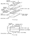
- FIG.3(a) is a perspective exploded view of the laminated dielectric resonator 220 according to the third embodiment of the present invention
- FIG.3(b) is a section, taken along a line X-X' in FIG.3(a)
- FIG.3(c) is an equivalent circuit diagram of the laminated dielectric resonator 220.
- FIGS.3(a), (b), a different point of the laminated dielectric resonator 220 from that of the first embodiment is that: one coupling electrode 13 is formed, as an external electrode, on the same surface as the surface of the dielectric sheet 5 at which the second shield electrode 7b is formed, and the coupling electrode 13 composes a capacitor together with the second strip line 4 to connect the resonator to the external circuit.
- the other construction is the same as that in the first embodiment.
- the end-short strip line resonator in which the first strip line 2 and the second strip line 4 are connected to each other is regarded as to compose a parallel resonator 14 which resonates in parallel at about the resonant frequency.
- the second strip line 4 and the coupling electrode 13 form a capacitor 15.
- the coupling electrode 13 serves as a terminal for connecting the laminated dielectric resonator to the external circuit.
- the laminated dielectric resonator 220 in the electrical characteristic, seen from the coupling electrode 13 has two resonances of series resonance and parallel resonance.
- the impedance is infinite at the parallel resonant frequency and is zero at the series resonant frequency.
- the laminated dielectric resonator 220 in this embodiment works as a single-step notch filter which damps signal component of the series resonant frequency.
- FIG.4(a) is a perspective exploded view of a laminated dielectric resonator according to a modified example of the third embodiment of the present invention
- FIG.4(b) is a section, taken along a line X-X' in FIG.4(a).
- one end of the first strip line 2 is connected to one end of the second strip line 4 via a plurality of through hole electrodes 62 to form a second side shield electrode 61 on the side of the laminated body on the side of the through hole electrodes 62.
- the end of the first strip line 2 and the end of the second strip line 4 are connected to each other via the plural through hole electrodes 62, which requires no extension of each strip line 2, 4 on the connected side (left end part in the figure) to the end of the dielectric sheets 1. 3.
- the second side shield electrode 61 is formed at the entire side surface of the laminated body on the connected side (i.e., side surface on through hole electrodes 62 side).
- FIG.5(a) is a perspective exploded view of a laminated dielectric resonator 230 according to another modified example of the third embodiment
- FIG.5(b) is a section, taken along a line X-X' in FIG.5(a).
- another dielectric sheet 43 is further laminated on the dielectric sheet 5 to compose a coupling electrode 13 as the internal electrode.
- the coupling electrode 13 is formed at the same printing process as the formation of the strip line, which leads accurate coupling electrode 13 with less characteristic fluctuation.
- one terminal electrode 41 is formed, as the external electrode, on the upper surface of the dielectric sheet 43.
- a side electrode 42 connects the coupling electrode 13 to the terminal electrode 41. Without the side electrode 42, the coupling electrode 13 and the terminal electrode 41 may be connected by a through hole.
- the equivalent circuit of this modified example is identical with that in FIG.4(c). Since size and shape of the terminal electrode 41 do not contribute to the capacity of the capacitor 15, no characteristic fluctuation due to change in shape of the terminal electrode 41 and implementation state of the laminated dielectric resonator to the circuit substrate is caused, which means easy handling of the laminated dielectric resonator in this modified example.
- the resonator whose characteristic is to have the two resonances of series and parallel resonances, seen from the coupling electrode 13, can be easily formed by forming the capacitor 15 between the second strip line 4 and the coupling electrode 13.
- FIG.6(a) is a perspective exploded view of the dielectric filter, which uses the laminated dielectric resonators 220 in the third embodiment, according to the fourth embodiment of the present invention.
- FIG.6(b) is an equivalent circuit diagram of the dielectric filter in this embodiment.
- Connection patterns 222, 223 and a ground pattern 227 are formed on an implemented substrate 221.
- the connection pattern 222 is connected to the coupling electrode 13 of a first laminated dielectric resonator 220a, to one end of an air-core coil 224 as an inductance and to one end of a chip capacitor 225.
- the connection pattern 223 on the implemented substrate 221 is connected to the coupling electrode 13 of a second laminated dielectric resonator 220b, to the other end of the air-core coil 224 and to one end of another chip capacitor 226.
- ground pattern 227 on the implemented substrate 221 is electrically connected to any among or all of the respective ground electrodes 8, the respective shield electrodes 7a, 7b and the respective side shield electrodes 17 of the laminated dielectric resonators 220a, 220b to be grounded.
- Each of the other ends of the chip capacitors 225, 226 is grounded, also.
- the equivalent circuit to the laminated dielectric resonators 220a, 220b is shown in FIG.3(c) which work as resonators having two resonances of series resonance and parallel resonance.
- the impedance of the resonator is zero at the series resonant frequency, so that the resonators in cascade connection via the air-core coil 224 compose a band elimination filter.
- the chip capacitors 225, 226 connected in parallel to the resonators are compose a low pass filter together with the air-core coil 224 connected between the resonators to damp harmonic signal component and the like.
- a chip capacitor corresponding to the capacitor 15, which is generally required in the band elimination filter, and connection pins for connecting the resonator to the chip capacitor are unnecessary.
- the side shield electrodes 17 formed on both sides of the laminated body completely shields the resonator. As a result, surplus connection between the resonators is obviated even the laminated dielectric resonators are arranged adjacently, thus obtaining a excellent filter characteristic.
- the band elimination filter is easily constructed, with results of easy manufacturing, cost reduction, and size reduction of the dielectric filter.
- the plural dielectric resonators 220a are cascade-connected via the air-core coil 224 (inductance), but may be cascade-connected directly without the air-core coil 224.
- the laminated dielectric resonator to be cascade-connected may be a conventional laminated dielectric resonator or a laminated dielectric resonator to be described later.
- FIG.7(a) is a perspective exploded view of a laminated dielectric resonator according to the fifth embodiment
- FIG.7(b) is a section, taken along a line X-X' in FIG.7(a). Wherein, the description is made, using the same references as in the first embodiment.
- reference numeral 1 denotes a first dielectric sheet
- 3 denotes a second dielectric sheet
- 18 denotes a third dielectric sheet
- 5 denotes another dielectric sheet.
- the low-temperature sintered dielectric ceramic used in the first embodiment is used for the dielectric sheets 1, 3, 18, 5.
- a third strip line 16 is formed on the third dielectric sheet 18 from one end to the other end of the third dielectric sheet 18 by means of thick-film printing of conductor such as silver paste, copper paste.
- the first dielectric sheet 1 is laminated on the third dielectric sheet 18 at which the third strip line is formed.
- the first strip line 2 is formed on the first dielectric sheet 1 from one end to the other end of the first dielectric sheet 1 by the same means as the above.
- the second dielectric sheet 3 is laminated on the first dielectric sheet 1 at which the first strip line 2 is formed.
- the second strip line 4 which has the same figure as that of the third strip line 16 is formed on the second dielectric sheet 4 from one end to the other end of the second dielectric sheet 4.
- each length of the third strip line 16 and the second strip line 4 is shorter than that of the first strip line 2.
- the dielectric sheet 5 is laminated on the second dielectric sheet 3.
- the thus laminated dielectric sheets 1, 3, 5, 18 are pressed and burnt concurrently with the internal electrodes interposed therebetween.
- the shield electrodes 7a, 7b respectively are formed, as external electrodes, on upper and lower surfaces of the thus burnt laminated body.
- the side shield electrodes 17 are respectively formed, as the external electrodes, on both sides of the laminated body.
- Respective one ends of the first strip line 2, the second strip line 4 and the third strip line 16 are connected to one another via the connection electrode 8 formed as the external electrode.
- the other end of the first strip line 2 is grounded via the ground electrode 9 formed as the external electrode.
- the external electrodes are formed in such a manner that silver paste mixed with glass frit for thick-film printing or the like is coated on the surface, then burnt.
- the connection electrode 8 also serves as a connection terminal to the external circuit.
- the laminated dielectric resonator with the above construction works as an end-short strip line resonator whose wave length is one fourth and in which the line is folded in two ways at an intermediate part on the open end side by connecting the respective one ends of the first strip line 2, the second strip line 4 and the third strip line 16 via the connection electrodes 8.
- the second strip line 4 and the third strip line 16 are connected in series to the first strip line 2, thereby the folded end-short strip line resonator is obtained, with reduced physical length of the resonator.
- the loading capacitance to be connected in parallel to the resonator is doubled compared with in the first embodiment. Since the second strip line 4 and the third strip line 16 are connected in parallel to each other, the characteristic impedance on the open end side of the resonator line is further lowered compared with that in the first embodiment. Thus, the length of the resonator is further reduced compared with that in the first embodiment.
- Each length of the first strip line 2 and the second strip line 4 is set as follows.
- the resonant frequency is 1300MHz and the unloaded Q is 110 when the second strip line 4 is 0.35 ⁇ L in length; and the resonant frequency is decreased to 1130MHz and unloaded Q is degraded to 96 when the second strip line 2 is 0.65 ⁇ L in length.
- the length of the second strip line 4 is preferable to be set to not exceeding 0.65 ⁇ L, preferably, set to be not exceeding 0.5 ⁇ L, and set to be not exceeding 0.35 ⁇ L for further high performance resonator. While, when the second strip line 4 is set to not exceeding 0.2 ⁇ L, the effect of lowering the resonant frequency in the present invention is decreased. Therefore, the length of the second strip line 4 is preferable to set to be more than 0.2 ⁇ L.
- the resonant frequency is further reduced without degradation of the unloaded Q, and the whole length of the resonator is further reduced.
- a capacitor electrode is added to the construction of the first embodiment.
- the construction of a laminated dielectric resonator having only the capacitor electrode is discussed first.
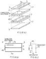
- FIG.8(a) is a perspective exploded view of the laminated dielectric resonator having the capacitor electrode
- FIG.8(b) is a section, taken along a line X-X' in FIG.8(a)
- FIG.8(c) is an equivalent circuit diagram of the laminated dielectric resonator.
- reference numeral 1 denotes a first dielectric sheet
- 3 denotes a second dielectric sheet
- 5 and 6 denote uppermost and lowermost dielectric sheets respectively.
- the same low-temperature sintered dielectric ceramic as in the first embodiment is used for these dielectric sheets 1, 3, 5, 6.
- the first dielectric sheet 1 is laminated on the lowermost dielectric sheet 6.
- the strip line 2 is formed on the upper surface of the first dielectric sheet 1 by means of thick-film printing of the conductor such as silver paste, copper paste.
- One end (left end in FIG.8(a)) of the strip line 2 is opened.
- the second dielectric sheet 3 is laminated on the first dielectric sheet 1 at which the strip line 2 is formed.
- the capacitor electrode 19 is formed on the upper surface of the second dielectric sheet 3 by the same means as the above so as to overlap the open end of the strip line 2.
- the capacitor electrode 19 extends to almost the center of the strip line 2 in the longitudinal direction.
- the uppermost dielectric sheet 5 is laminated on the second dielectric sheet 3.
- All dielectric sheets 1, 3, 5, 6 laminated are pressed and burnt concurrently with the internal electrodes interposed therebetween.
- First and second shield electrodes 7a, 7b are respectively formed, as the external electrodes, at the upper and lower surfaces of the thus burnt laminated body.
- the side shield electrodes 17 as the ground electrodes are formed, as the external electrodes, on both sides of the thus burnt laminated body (i.e., laminated body of four dielectric sheets 1, 3, 5, 6) in the width direction of the strip line 2.
- the ground electrode 9 is formed, as the external electrode, on one entire side surface of the thus burnt laminated body in the longitudinal direction of the strip line 2, and the connection terminal 45 to the external circuit is formed, as the external electrode, on the other side surface thereof in the longitudinal direction of the strip line 2.
- the capacitor electrode 19 is grounded via the side shield electrodes 17, and one end of the strip line 2 (right end in FIG.8(a)) is grounded via the ground electrode 9. The other end of the strip line 2 (left end in FIG.8(a)) is opened and connected to the connection terminal 45.
- Each external electrode is formed in such a manner that the silver paste mixed with glass frit for thick-film printing is coated on the surface, then burnt.
- the end-short strip line resonator composed of the strip line 2 is regarded as to compose the parallel resonator 14 which resonates in parallel at about the resonant frequency.
- the strip line 2 and the capacitor electrode 19 compose the capacitor 20.
- the capacitor 20 is connected, as a loading capacitor, in parallel to the resonator 14 equivalently composed of the end-short strip line resonator. Accordingly, as the capacitance component of the resonator increases, the resonant frequency is lowered and the length of the resonator can be reduced.
- the resonator composed of the strip line 2 is in SIR structure in which the impedance is changed in steps at the intermediate of the line, with a result of further decrease in resonant frequency.
- dielectric material with less relative permittivity can be used as the resonant frequency is lowered. Therefore, the dielectric material with less dielectric loss tangent can be used without elongating the physical length of the resonator, improving the unloaded Q thereof.
- the capacitor electrode 19 extends from the open end side to almost the center in the longitudinal direction of the strip line to cover the strip line 2, the capacitance component to be connected in parallel to the resonator becomes large and the resonant frequency of the resonator is further lowered, reducing the length of the resonator. Further, the electric field energy component is large at the open end side of the strip line and magnetic field energy component is large at the grounded end side thereof in the electromagnetic field distribution in the resonator. Therefore, in case where the capacitor electrode 19 is larger than one half of the whole length of the strip line 2, the effect of the length reduction is less and high-frequency current induced by the magnetic field energy flows to the capacitor electrode 19 to causes disadvantages of increased resistance loss and degradation of unloaded Q of the resonator.
- the side shield electrodes 17 formed on both sides of the laminated body shield completely the both side surfaces of the resonator, electromagnetic interference between the laminated dielectric resonator and the external circuit and connection between the adjacently arranged resonators are prevented.
- the side shield electrodes 17 work to compellingly equalize the potential of the open end of the upper shield electrode 7 to the ground potential by connecting the upper and lower shield electrodes 7 to each other, thus preventing the shield electrodes 7 from unnecessary resonance at about the resonant frequency of the strip line resonator.
- the side shield electrodes 17, as the external electrode, formed on both sides of the laminated body the resonator with excellent shield characteristic and excellent resonant characteristic is obtained.
- the capacitance of the capacitor 20 by adjusting the area of the capacitor electrode 19, the resonant frequency of the resonator is easily changed and adjusted, remaining the figure of the strip line 2 unchanged. This facilitates layout of the resonator.
- FIG.9(a) is a perspective exploded view of another laminated dielectric resonator having a capacitor electrode
- FIG.9(b) is a section, taken along a line X-X' in FIG.9(a)
- FIG.9(c) is an equivalent circuit diagram of the laminated dielectric resonator in this embodiment.
- reference numeral 1 denotes a first dielectric sheet
- 3 denotes a second dielectric sheet
- 48 denotes a third dielectric sheet
- 5 denotes another dielectric sheet.
- the same low-temperature sintered dielectric ceramic as in the first embodiment is used for these dielectric sheets 1, 3, 48, 5.
- a second capacitor electrode 22 is formed on the third dielectric sheet 48 by means of thick-film printing of the conductor such silver paste, copper paste.
- the first dielectric sheet 1 is laminated on the third dielectric sheet 48 at which the second capacitor electrode 22 is formed, and a strip line 21 is formed on the upper surface of the first dielectric sheet 1 by the means as the above.
- the strip line 21 is formed in such a fashion that one end thereof (left end in FIG.9(a)) is wide to be a wide part 21a and the other end thereof is narrow to be a narrow part 21b, in which the line width is made narrow from the intermediate part of the strip line 21.
- the second dielectric sheet 3 is laminated on the first dielectric sheet 1 at which the strip line 21 is formed, and the first capacitor electrode 19 is formed on the upper surface of the second dielectric sheet 3.
- the first capacitor electrode 19 and the second capacitor electrode 22 are formed so as to overlap one open end of the strip line 21 under condition that first to third dielectric sheets 1, 3, 48 are laminated.
- the other dielectric sheet 5 is laminated on the second dielectric sheet 3 at which the first capacitor electrode 19 is formed. These four dielectric sheets 1, 3, 5, 48 laminated are pressed, and burnt concurrently with the internal electrode interposed therebetween.
- the first shield electrode 7a and the second shield electrode 7b are respectively formed, as the external electrodes, on upper and lower surfaces of the thus burnt laminated body, i.e., the lower surface of the third dielectric sheet 48 and the upper surface of the other dielectric sheet 5.
- the side shield electrode 17 is formed as the external electrode
- the ground electrode 9 is formed, as the external electrode, on one side surface in the longitudinal direction.
- the first capacitor electrode 19 and the second capacitor electrode 22 are grounded via the side shield electrodes 17 as the ground electrodes, and the other end (right end in FIG.9(a)) of the strip line 21 is grounded via the ground electrode 9.
- the connection terminal 45 to the external circuit is provided as the external electrode.
- Each external electrode is formed in such a manner that the silver paste mixed with glass frit for thick-film printing is coated on the surface, then burnt.
- the end-short strip line resonator composed of the strip line 21 can be regarded as to construct the parallel resonator 14 which resonates in parallel at about the resonant frequency.
- the capacitor 20 is formed by the strip line 21 and the capacitor electrode 19, and the capacitor 23 is formed by the strip line 21 and the capacitor electrode 22. Accordingly, in this construction, since the capacitors 20, 23 are connected, as the loading capacitors, in parallel to the resonator 14 equivalently composed of the end-short strip line resonator, the resonant frequency is lowered as the capacitance component of the resonator increases, thus reducing the length of the resonator. Also, in this construction, the loading capacitor to be connected in parallel to the resonator is doubled compared with that in the sixth embodiment. As a result, the resonant frequency of the resonator in this embodiment is lower than that in the sixth embodiment.
- the impedance step ratio of the SIR type resonator becomes further large.
- the characteristic impedance of the strip line 21 is larger at the grounded end than at the open end, the length of the strip line 21 is further reduced.
- the resonator with the above construction can further lower of the resonant frequency and further reduce the whole length thereof, in addition to the same effects as in the sixth embodiment.
- FIG.10(a) is a perspective exploded view of the laminated dielectric resonator in the sixth embodiment and FIG.9(b) is a section, taken along a line X-X' in FIG.9(a).
- reference numeral 1 denotes a first dielectric sheet
- 3 denotes a second dielectric sheet
- 18 denotes a third dielectric sheet
- 5 and 6 denote uppermost and lowermost dielectric sheets respectively.
- the same low-temperature sintered dielectric ceramic as in the first embodiment is used for these dielectric sheets 1, 3, 18, 5, 6.
- the first dielectric sheet 1 is laminated on the dielectric sheet 6.
- the first strip line 2 is formed on the upper surface of the first dielectric sheet 1 by means of thick-film printing of the conductor such as silver paste, copper paste so as to extent from one end to the other end of the first dielectric sheet 1.
- the second dielectric sheet 3 is laminated on the first dielectric sheet 1 at which the first strip line 2 is formed, and the capacitor electrode 19 is formed on the upper surface of the second dielectric sheet 3 by the same means as the above.
- the third dielectric sheet 18 is laminated on the second dielectric sheet 3 at which the capacitor electrode 19 is formed.
- the second strip line 4 shorter than the first strip line 2 is formed on the upper surface of the third dielectric sheet 18 so as to extend from one end to the other end of the third dielectric sheet 18.
- the capacitor electrode 19 is formed so as to overlap the region thereof with the first strip line 2 and the second strip line 4 under the condition that first to third dielectric sheets 1, 3, 18 are laminated.
- the dielectric sheet 5 is laminated on the third dielectric sheet 18 at which the second strip line 4 is formed. Each dielectric sheet laminated is pressed, and burnt concurrently with the internal electrodes interposed therebetween.
- the first shield electrode 7a and the second shield electrode 7b are respectively formed, as the external electrodes, on upper and lower surfaces of the thus burnt laminated body, i.e., the lower surface the lowermost dielectric sheet 6 and the upper surface of the uppermost dielectric sheet 5.
- the side shield electrodes 17 are respectively formed as the external electrode, and the capacitor electrode 19 is grounded via the side shield electrodes 17.
- the ground electrode 9 is formed, as the external electrode, on one side of the thus burnt laminated body in the longitudinal direction, and one end of the first strip line 2 is connected to the ground electrode 9.
- the connection electrode 8 is formed, as the external electrode, on the other side of first to third dielectric sheets 1, 3, 18 in the longitudinal direction, and the other end of the first strip line 2 and one end of the second strip line 4 are connected to each other via the connection electrode 8.
- Each external electrode is formed in such a manner that the silver paste mixed with glass frit for thick-film printing is coated on the surface, then burnt.
- the connection electrode 8 is used also for the connection terminal to the external circuit.
- the operation principle of the laminated dielectric resonator with the above construction is explained by a combination of the operation principles of the laminated dielectric resonator in the first embodiment and the laminated dielectric resonator having the capacitor electrode in FIG.7. Therefore, in this embodiment, the resonant frequency is further lowered by the combination of the effects of the first embodiment and the laminated dielectric resonator in FIG.7, which reduces the length of the resonator further.
- the capacitor electrode 19 is formed between the first strip line 2 and the second strip line 4, the loading capacitance is formed between the second strip line 4 and the capacitor electrode 19 as well as between the first strip line 2 and the capacitor electrode 19, thus enlarging the loading capacitance. Consequently, the resonant frequency is further lowered.
- the loading capacitance can be enlarged, lowering the resonant frequency and reducing the whole length of the resonator.
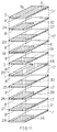
- FIG.11 is a perspective exploded view of the laminated dielectric resonator in the seventh embodiment
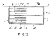
- FIG.12 is a section, taken along a line X-X' in FIG.11.
- the basic construction of the laminated dielectric resonator in this embodiment is a combination of the foregoing laminated dielectric resonators.
- reference numerals 1, 3, 5, 18, 23, 24, 25, 26, 27, 28 denote dielectric sheets.
- the same low-temperature sintered dielectric ceramic as in the first embodiment is used for the dielectric sheets 1, 3, 5, 18, 23, 24, 25, 26, 27, 28.
- the first strip line 29 is formed on the first dielectric sheet 1 so as to extend from one end to the other end of the first dielectric sheet 1.
- First, second, third and fourth capacitor electrodes 19, 22, 30, 31 are formed respectively on second, fourth, sixth and eighth dielectric sheets 3, 23, 25, 27.
- Second, third, fourth and fifth strip lines 4, 32, 33, 34 which are shorter than the first strip line 29 are respectively formed on third, fifth, seventh and ninth dielectric sheets 18, 24, 26, 28 so as to extend from one end to the other end of the respective dielectric sheets 18, 24, 26, 28.
- An electrode region 44 whose line width is equal to the width of the first dielectric sheet 1 is formed at the other end (right end in FIG.11) of the first strip line 29.
- the ninth dielectric sheet 28, the eight dielectric sheet 27, the seventh dielectric sheet 26, the sixth dielectric sheet 25, the first dielectric sheet 1, the second dielectric sheet 3, the third dielectric sheet 18, the fourth dielectric sheet 23, the fifth dielectric sheet 24, and another dielectric sheet 5 are overlaid in this order.
- the capacitor electrode 19 is so formed that the region thereof overlaps with the first strip line 29 and the second strip line 4 under the laminated condition of the dielectric sheets
- the capacitor electrode 30 is so formed that the region thereof overlaps with the first strip line 29 and the fourth strip line 33 under the laminated condition of dielectric sheets.
- the capacitor electrode 22 is so formed that the region thereof overlaps with the second strip line 4 and the third strip line 32
- the capacitor electrode 31 is so formed that the region thereof overlaps with the fourth strip line 33 and the fifth strip line 34.
- the respective dielectric sheets laminated are pressed, and burnt concurrently with the internal electrodes.
- first and second shield electrodes 7a, 7b are respectively formed as the external electrodes.
- the side shield electrodes 17 are respectively formed, as the external electrodes, on both sides of the thus burnt laminated body in the width direction, and the capacitor electrodes 19, 22, 30, 31 are grounded via the side shield electrodes 17.
- the connection electrode 8 is formed, as the external electrode, on one side surface of the thus burnt laminated body in the longitudinal direction, and one end of the first strip line 29 is connected via the connection electrode 8 to each one end of second, third, fourth and fifth strip lines 4, 32, 33, 34.
- the ground electrode 9 is formed, as the external electrode, to ground the electrode region 44 of the first strip line 29.
- Each external electrode is formed in such a manner that the silver paste mixed with glass frit for thick-film printing is coat on the surface, then burnt.
- the connection electrode 8 serves as also the connection terminal to the external circuit.
- the operation principle of the thus constructed laminated dielectric resonator is basically the same as that of the laminated dielectric resonator in the sixth embodiment.
- the construction in the sixth embodiment is laminated repeatedly in up and down direction for increasing the effects of the sixth embodiment.
- the electrode region 44 wider than the width of the first strip line 29 is provided on the grounded end side of the first strip line 29, and the first strip line 29 is connected and grounded, via the electrode region 44, to the ground electrode 9 or the side shield electrodes 17.
- the first strip line 29 is grounded positively, eliminating surplus inductance component and resistance component, which prevents fluctuation of the resonant frequency of the resonator and improves the unloaded Q.
- the length of the resonator is further reduced with large loading capacitance. Further, the connection of the grounded end of the strip line 29 is ensured, so that the laminated dielectric resonator with less fluctuation of the resonant frequency and high unloaded Q is attained.
- FIG.13(a) is a perspective view of the laminated dielectric resonator 110 in the eighth embodiment
- FIG.13(b) is a section, taken along a line X-X' in FIG.13(a)
- FIG.13(c) is an equivalent circuit diagram of the laminated dielectric resonator 110 in this embodiment.
- two coupling electrodes 13a, 13b are formed, as the external electrodes, on the surface, and compose a capacitor together with the second strip line 4, so that the capacitor connects the resonator to the external circuit.
- the other construction is the same as in the fifth embodiment.
- the second strip line 4 and the coupling electrodes 13a, 13b form the capacitors 15a, 15b.
- the coupling electrodes 13a, 13b serve as input/output terminals for connecting the laminated dielectric resonator to the external circuit.
- This circuit has a characteristic of single-step band pass filter in which the capacitors 15a, 15b serve input/output coupling capacitors of the parallel resonant circuit.
- the simple single-pole band pass filter is easily constructed with the capacitors 15a, 15b respectively formed between the second strip line 4 and the coupling electrodes 13a, 13b, besides the same effects and features as in the fifth embodiment.
- FIG.14(a) is a perspective exploded view of a laminated dielectric filter according to the ninth embodiment, in which the laminated dielectric resonators 110 in the eighth embodiment are connected in multi-pole to one another.
- connection patterns 112, 113, 114 and a ground pattern 115 are formed on an implemented substrate 111.
- a coupling electrode 13a of a first laminated dielectric resonator 110a is connected to the connection pattern 112.
- the coupling electrode 13b of the first laminated dielectric resonator 110a and a coupling electrode 13b of a second laminated dielectric resonator 110b are connected to the connection pattern 113.
- a coupling electrode 13a of the second laminated dielectric resonator 110b is connected to the connection pattern 114.
- To the ground pattern 115 all of or any among the respective ground electrodes 8, the respective shield electrodes 7 and the respective side shield electrodes 17 of the laminated dielectric resonators 110a, 110b are/is electrically connected.
- the respective capacitors 15b of the laminated dielectric resonators 110a, 110b are connected in series to each other to work as inter-resonator coupling capacitors.
- the respective capacitors 15a of the laminated dielectric resonators 110a, 110b work as input/output coupling capacitors. Accordingly, a multi-pole filter of capacitance coupling type is constructed, with a result of a multi-pole band pass filter having excellent selection characteristic, e.g. Tchebysheff characteristic.
- the resonator is completely shielded, with a result that excellent filter characteristic is obtained without extra joint between the resonators even though the laminated dielectric resonators are arranged adjacently.
- the multi-step band pass filter with excellent selection characteristic is easily obtained.
- the chip condensers and connection pins required for the conventional band pass filter is unnecessary, thus facilitating the manufacturing process and reducing the cost and size of the dielectric filter.
- the present invention is applicable to a case where two or more strip line resonators are formed thereon.
- the strip line resonators are connected in electromagnetic field to one another to compose the filter by the thus connected body.
- This invention is effective as a technique for reducing the length of each strip line resonator composing the filter.
- the invention includes, of course, a laminated dielectric filter with such a construction.
- the laminated dielectric resonator is applied to the dielectric filter only.
- the laminated dielectric resonator in this invention may be used as a resonant element for stabilizing oscillation frequency of a high-frequency oscillation circuit such as voltage controlled oscillator (VCO).
- VCO voltage controlled oscillator
Landscapes
- Physics & Mathematics (AREA)
- Electromagnetism (AREA)
- Control Of Motors That Do Not Use Commutators (AREA)
Applications Claiming Priority (2)
| Application Number | Priority Date | Filing Date | Title |
|---|---|---|---|
| JP66315/93 | 1993-03-25 | ||
| JP6631593 | 1993-03-25 |
Publications (2)
| Publication Number | Publication Date |
|---|---|
| EP0617478A1 true EP0617478A1 (fr) | 1994-09-28 |
| EP0617478B1 EP0617478B1 (fr) | 1998-07-29 |
Family
ID=13312280
Family Applications (1)
| Application Number | Title | Priority Date | Filing Date |
|---|---|---|---|
| EP94104729A Expired - Lifetime EP0617478B1 (fr) | 1993-03-25 | 1994-03-24 | Résonateur diélectrique stratifié et filtre diélectrique |
Country Status (3)
| Country | Link |
|---|---|
| US (3) | US5479141A (fr) |
| EP (1) | EP0617478B1 (fr) |
| DE (1) | DE69411973T2 (fr) |
Cited By (7)
| Publication number | Priority date | Publication date | Assignee | Title |
|---|---|---|---|---|
| EP0785593A1 (fr) | 1996-01-18 | 1997-07-23 | Lk-Products Oy | Construction de résonateur diélectrique et filtre diélectrique à longueur physique réduite |
| WO1998027607A1 (fr) * | 1996-12-18 | 1998-06-25 | Siemens Aktiengesellschaft | Filtre hyperfrequence |
| EP0820115A3 (fr) * | 1996-07-15 | 1998-12-23 | Matsushita Electric Industrial Co., Ltd. | Dispositif diélectrique multicouche et procédé de fabrication |
| EP0862238A3 (fr) * | 1997-02-26 | 1999-06-23 | Ngk Spark Plug Co., Ltd. | Circuit multi-couche microélectronique |
| EP0837517A3 (fr) * | 1996-10-18 | 2000-08-09 | Matsushita Electric Industrial Co., Ltd. | Filtre diélectrique statifié et dispositif de communication |
| CN1099717C (zh) * | 1994-12-19 | 2003-01-22 | 皇家菲利浦电子有限公司 | 带状线滤波器,具有带状线滤波器的接收机及调谐带状线滤波器的方法 |
| CN113330633A (zh) * | 2019-01-15 | 2021-08-31 | 瑞典爱立信有限公司 | 天线系统的微型滤波器设计 |
Families Citing this family (29)
| Publication number | Priority date | Publication date | Assignee | Title |
|---|---|---|---|---|
| US5479141A (en) * | 1993-03-25 | 1995-12-26 | Matsushita Electric Industrial Co., Ltd. | Laminated dielectric resonator and dielectric filter |
| JPH07263901A (ja) * | 1994-03-24 | 1995-10-13 | Murata Mfg Co Ltd | 高周波部品 |
| US5825264A (en) * | 1994-05-18 | 1998-10-20 | Fdk Corporation | Stripline laminate dielectric filter with input/output patterns overlapping resonator conductors |
| JP3185607B2 (ja) * | 1995-05-31 | 2001-07-11 | 株式会社村田製作所 | 表面実装型アンテナおよびこれを用いた通信機 |
| JP3243595B2 (ja) * | 1995-10-31 | 2002-01-07 | 株式会社トーキン | マルチバンドアンテナ及びそれを用いたマルチバンド携帯無線機 |
| JPH1032429A (ja) * | 1996-07-18 | 1998-02-03 | Matsushita Electric Ind Co Ltd | 電圧制御共振器およびその調整方法 |
| EP0943157A4 (fr) * | 1996-10-31 | 2000-05-24 | Sarnoff Corp | Circuit electronique integre |
| US5834994A (en) * | 1997-01-17 | 1998-11-10 | Motorola Inc. | Multilayer lowpass filter with improved ground plane configuration |
| US5818313A (en) * | 1997-01-31 | 1998-10-06 | Motorola Inc. | Multilayer lowpass filter with single point ground plane configuration |
| US6329890B1 (en) * | 1999-02-25 | 2001-12-11 | Thin Film Technology Corp. | Modular thin film distributed filter |
| US6518863B2 (en) * | 2000-05-25 | 2003-02-11 | Matsushita Electric Industrial Co., Ltd. | Dielectric laminated device and manufacturing method thereof |
| US20020158305A1 (en) * | 2001-01-05 | 2002-10-31 | Sidharth Dalmia | Organic substrate having integrated passive components |
| US6704248B1 (en) * | 2001-05-25 | 2004-03-09 | Lockheed Martin Corporation | High density power module incorporating passive components distributed in a substrate |
| US6987307B2 (en) * | 2002-06-26 | 2006-01-17 | Georgia Tech Research Corporation | Stand-alone organic-based passive devices |
| US6900708B2 (en) * | 2002-06-26 | 2005-05-31 | Georgia Tech Research Corporation | Integrated passive devices fabricated utilizing multi-layer, organic laminates |
| US7260890B2 (en) * | 2002-06-26 | 2007-08-28 | Georgia Tech Research Corporation | Methods for fabricating three-dimensional all organic interconnect structures |
| US7489914B2 (en) * | 2003-03-28 | 2009-02-10 | Georgia Tech Research Corporation | Multi-band RF transceiver with passive reuse in organic substrates |
| JP4186986B2 (ja) * | 2003-06-18 | 2008-11-26 | 株式会社村田製作所 | 共振器、フィルタおよび通信装置 |
| US8345433B2 (en) * | 2004-07-08 | 2013-01-01 | Avx Corporation | Heterogeneous organic laminate stack ups for high frequency applications |
| JP4432119B2 (ja) * | 2005-09-15 | 2010-03-17 | 大同特殊鋼株式会社 | バンドパスフィルター |
| JP4172654B2 (ja) * | 2006-02-17 | 2008-10-29 | Tdk株式会社 | 薄膜デバイス |
| JP4539870B2 (ja) * | 2006-03-31 | 2010-09-08 | Tdk株式会社 | 薄膜デバイス |
| US7439840B2 (en) | 2006-06-27 | 2008-10-21 | Jacket Micro Devices, Inc. | Methods and apparatuses for high-performing multi-layer inductors |
| US7808434B2 (en) * | 2006-08-09 | 2010-10-05 | Avx Corporation | Systems and methods for integrated antennae structures in multilayer organic-based printed circuit devices |
| US7989895B2 (en) * | 2006-11-15 | 2011-08-02 | Avx Corporation | Integration using package stacking with multi-layer organic substrates |
| JP4962565B2 (ja) * | 2007-04-27 | 2012-06-27 | 株式会社村田製作所 | 共振素子および、その製造方法 |
| KR101295869B1 (ko) * | 2009-12-21 | 2013-08-12 | 한국전자통신연구원 | 복수의 절연층들에 형성된 선로 필터 |
| KR101430684B1 (ko) * | 2013-04-12 | 2014-08-14 | 주식회사 이너트론 | 공진 소자 및 이를 이용한 필터 |
| CN119547392A (zh) * | 2022-08-25 | 2025-02-28 | 瑞典爱立信有限公司 | 多频带滤波器及通信装置 |
Citations (4)
| Publication number | Priority date | Publication date | Assignee | Title |
|---|---|---|---|---|
| GB708597A (en) * | 1951-05-23 | 1954-05-05 | Standard Telephones Cables Ltd | Radio frequency filter |
| JPS63128801A (ja) * | 1986-11-19 | 1988-06-01 | Matsushita Electric Ind Co Ltd | 濾波器 |
| DE4203939A1 (de) * | 1991-02-15 | 1992-08-27 | Murata Manufacturing Co | Bandpassfilter |
| EP0506476A1 (fr) * | 1991-03-29 | 1992-09-30 | Ngk Insulators, Ltd. | Filtre diélectrique avec des électrodes de couplage pour relier des résonateurs ou des électrodes, et méthode pour ajuster la caractéristique de fréquence du filtre |
Family Cites Families (16)
| Publication number | Priority date | Publication date | Assignee | Title |
|---|---|---|---|---|
| JPS55100701A (en) * | 1979-01-26 | 1980-07-31 | Matsushita Electric Ind Co Ltd | Coaxial resonator |
| JPH01222501A (ja) * | 1988-03-01 | 1989-09-05 | Nec Corp | 高周波回路 |
| JP2740966B2 (ja) * | 1989-02-28 | 1998-04-15 | 住友金属工業株式会社 | 高周波誘電体部品およびその製造方法 |
| JPH0693589B2 (ja) * | 1989-03-23 | 1994-11-16 | 株式会社村田製作所 | Lcフィルター |
| JP2662741B2 (ja) * | 1990-03-05 | 1997-10-15 | 株式会社村田製作所 | 共振器 |
| US5246220A (en) * | 1990-12-14 | 1993-09-21 | Fuji Photo Film Co., Ltd. | Sheet feeding device |
| JP2707851B2 (ja) * | 1991-02-28 | 1998-02-04 | 株式会社村田製作所 | 電磁干渉フィルタ |
| JP2502824B2 (ja) * | 1991-03-13 | 1996-05-29 | 松下電器産業株式会社 | 平面型誘電体フィルタ |
| JP2606044B2 (ja) * | 1991-04-24 | 1997-04-30 | 松下電器産業株式会社 | 誘電体フィルタ |
| US5300903A (en) * | 1991-06-27 | 1994-04-05 | Murata Manufacturing Co., Ltd. | Band-pass filter |
| US5382425A (en) * | 1992-01-13 | 1995-01-17 | Syntro Corporation | Recombinant swinepox virus |
| US5374909A (en) * | 1992-02-28 | 1994-12-20 | Ngk Insulators, Ltd. | Stripline filter having internal ground electrodes |
| DE69321907T2 (de) * | 1992-03-19 | 1999-04-22 | Tdk Corp., Tokio/Tokyo | Hybrider koppler |
| US5404118A (en) * | 1992-07-27 | 1995-04-04 | Murata Manufacturing Co., Ltd. | Band pass filter with resonator having spiral electrodes formed of coil electrodes on plurality of dielectric layers |
| JP2824370B2 (ja) * | 1992-10-09 | 1998-11-11 | 三菱電機株式会社 | 位相同期ループ回路 |
| US5479141A (en) * | 1993-03-25 | 1995-12-26 | Matsushita Electric Industrial Co., Ltd. | Laminated dielectric resonator and dielectric filter |
-
1994
- 1994-03-24 US US08/217,118 patent/US5479141A/en not_active Expired - Lifetime
- 1994-03-24 EP EP94104729A patent/EP0617478B1/fr not_active Expired - Lifetime
- 1994-03-24 DE DE69411973T patent/DE69411973T2/de not_active Expired - Lifetime
-
1995
- 1995-09-22 US US08/532,304 patent/US5644275A/en not_active Expired - Lifetime
- 1995-09-22 US US08/532,303 patent/US5654681A/en not_active Expired - Lifetime
Patent Citations (4)
| Publication number | Priority date | Publication date | Assignee | Title |
|---|---|---|---|---|
| GB708597A (en) * | 1951-05-23 | 1954-05-05 | Standard Telephones Cables Ltd | Radio frequency filter |
| JPS63128801A (ja) * | 1986-11-19 | 1988-06-01 | Matsushita Electric Ind Co Ltd | 濾波器 |
| DE4203939A1 (de) * | 1991-02-15 | 1992-08-27 | Murata Manufacturing Co | Bandpassfilter |
| EP0506476A1 (fr) * | 1991-03-29 | 1992-09-30 | Ngk Insulators, Ltd. | Filtre diélectrique avec des électrodes de couplage pour relier des résonateurs ou des électrodes, et méthode pour ajuster la caractéristique de fréquence du filtre |
Non-Patent Citations (1)
| Title |
|---|
| PATENT ABSTRACTS OF JAPAN vol. 12, no. 385 (E - 668) 14 October 1988 (1988-10-14) * |
Cited By (16)
| Publication number | Priority date | Publication date | Assignee | Title |
|---|---|---|---|---|
| CN1099717C (zh) * | 1994-12-19 | 2003-01-22 | 皇家菲利浦电子有限公司 | 带状线滤波器,具有带状线滤波器的接收机及调谐带状线滤波器的方法 |
| EP0785593A1 (fr) | 1996-01-18 | 1997-07-23 | Lk-Products Oy | Construction de résonateur diélectrique et filtre diélectrique à longueur physique réduite |
| US6310525B1 (en) | 1996-07-15 | 2001-10-30 | Matsushita Electric Industrial Co. Ltd. | Dielectric laminated device and its manufacturing method |
| US6765460B2 (en) | 1996-07-15 | 2004-07-20 | Matsushita Electric Industrial Co., Ltd. | Dielectric laminated device including a buried electric conductive member to form a strip line and its method of manufacture |
| US6020798A (en) * | 1996-07-15 | 2000-02-01 | Matsushita Electric Industrial Co., Ltd. | Dielectric laminated device and its manufacturing method |
| US6941650B2 (en) | 1996-07-15 | 2005-09-13 | Matsushita Electric Industrial Co., Ltd. | Method for manufacturing dielectric laminated device |
| US6510607B1 (en) | 1996-07-15 | 2003-01-28 | Matsushita Electric Industrial Co., Ltd. | Method for forming a dielectric laminated device |
| US6346866B2 (en) | 1996-07-15 | 2002-02-12 | Matsushita Electric Industrial Co., Ltd. | Dielectric laminated device and its manufacturing method |
| EP0820115A3 (fr) * | 1996-07-15 | 1998-12-23 | Matsushita Electric Industrial Co., Ltd. | Dispositif diélectrique multicouche et procédé de fabrication |
| EP0837517A3 (fr) * | 1996-10-18 | 2000-08-09 | Matsushita Electric Industrial Co., Ltd. | Filtre diélectrique statifié et dispositif de communication |
| US6265954B1 (en) | 1996-12-18 | 2001-07-24 | Siemens Aktiengesellschaft | Microwave filter |
| WO1998027607A1 (fr) * | 1996-12-18 | 1998-06-25 | Siemens Aktiengesellschaft | Filtre hyperfrequence |
| EP0862238A3 (fr) * | 1997-02-26 | 1999-06-23 | Ngk Spark Plug Co., Ltd. | Circuit multi-couche microélectronique |
| US6046409A (en) * | 1997-02-26 | 2000-04-04 | Ngk Spark Plug Co., Ltd. | Multilayer microelectronic circuit |
| CN113330633A (zh) * | 2019-01-15 | 2021-08-31 | 瑞典爱立信有限公司 | 天线系统的微型滤波器设计 |
| CN113330633B (zh) * | 2019-01-15 | 2023-06-23 | 瑞典爱立信有限公司 | 微型天线滤波器及滤波器阵列 |
Also Published As
| Publication number | Publication date |
|---|---|
| US5479141A (en) | 1995-12-26 |
| DE69411973D1 (de) | 1998-09-03 |
| EP0617478B1 (fr) | 1998-07-29 |
| US5654681A (en) | 1997-08-05 |
| US5644275A (en) | 1997-07-01 |
| DE69411973T2 (de) | 1998-12-10 |
Similar Documents
| Publication | Publication Date | Title |
|---|---|---|
| EP0617478B1 (fr) | Résonateur diélectrique stratifié et filtre diélectrique | |
| EP1742354B1 (fr) | Filtre passe-bande multicouche | |
| EP0336255B1 (fr) | Filtre monté sur la surface, avec une connexion sous forme de ligne de transmission intégrée | |
| KR0147726B1 (ko) | 유전체 필터 | |
| EP0566145A2 (fr) | Filtre passe-bas à haute fréquence | |
| US8294532B2 (en) | Duplex filter comprised of dielectric cores having at least one wall extending above a top surface thereof for isolating through hole resonators | |
| EP1265312B1 (fr) | Filtre diélectrique stratifié éliminateur de bande avec couplage électromagnétique entre résonateurs | |
| CN100433323C (zh) | 高频开关组件 | |
| US20020101303A1 (en) | Multilayer LC composite component | |
| JPH0730305A (ja) | 誘電体フィルターおよび誘電体フィルターを用いたトランシーバー | |
| US5311159A (en) | Bandpass type filter having tri-plate line resonators | |
| US9030272B2 (en) | Duplex filter with recessed top pattern and cavity | |
| US12506239B2 (en) | Dielectric filter | |
| JP3329450B1 (ja) | 誘電体装置 | |
| US6885261B2 (en) | Dielectric filter, antenna sharing device, and communication device having a voltage controlled reactance element for tuning the center frequency | |
| US5977848A (en) | Polar dielectric filter and dielectric duplexer incorporating same | |
| JPH07226602A (ja) | 積層型誘電体フィルタ | |
| JPH05218705A (ja) | 積層型帯域除去フィルター | |
| US20060164182A1 (en) | Surface acoustic wave filter | |
| JP3464820B2 (ja) | 誘電体積層共振器および誘電体フィルタ | |
| JP2710904B2 (ja) | 積層型誘電体フィルタ | |
| JP2000091807A (ja) | 誘電体バンドパス・フィルタ | |
| KR100258788B1 (ko) | 동축선 공진기의 절반구조를 이용한 대역 통과 여파기 | |
| JP2002111305A (ja) | 周波数可変複合フィルタ | |
| JPH0846403A (ja) | 誘電体フィルタ用基板及び誘電体フィルタ |
Legal Events
| Date | Code | Title | Description |
|---|---|---|---|
| PUAI | Public reference made under article 153(3) epc to a published international application that has entered the european phase |
Free format text: ORIGINAL CODE: 0009012 |
|
| AK | Designated contracting states |
Kind code of ref document: A1 Designated state(s): DE FR GB |
|
| 17P | Request for examination filed |
Effective date: 19941220 |
|
| 17Q | First examination report despatched |
Effective date: 19970129 |
|
| GRAG | Despatch of communication of intention to grant |
Free format text: ORIGINAL CODE: EPIDOS AGRA |
|
| GRAG | Despatch of communication of intention to grant |
Free format text: ORIGINAL CODE: EPIDOS AGRA |
|
| GRAH | Despatch of communication of intention to grant a patent |
Free format text: ORIGINAL CODE: EPIDOS IGRA |
|
| GRAH | Despatch of communication of intention to grant a patent |
Free format text: ORIGINAL CODE: EPIDOS IGRA |
|
| GRAA | (expected) grant |
Free format text: ORIGINAL CODE: 0009210 |
|
| AK | Designated contracting states |
Kind code of ref document: B1 Designated state(s): DE FR GB |
|
| REF | Corresponds to: |
Ref document number: 69411973 Country of ref document: DE Date of ref document: 19980903 |
|
| ET | Fr: translation filed | ||
| PLBE | No opposition filed within time limit |
Free format text: ORIGINAL CODE: 0009261 |
|
| STAA | Information on the status of an ep patent application or granted ep patent |
Free format text: STATUS: NO OPPOSITION FILED WITHIN TIME LIMIT |
|
| 26N | No opposition filed | ||
| REG | Reference to a national code |
Ref country code: GB Ref legal event code: IF02 |
|
| PGFP | Annual fee paid to national office [announced via postgrant information from national office to epo] |
Ref country code: GB Payment date: 20130320 Year of fee payment: 20 Ref country code: FR Payment date: 20130325 Year of fee payment: 20 Ref country code: DE Payment date: 20130320 Year of fee payment: 20 |
|
| REG | Reference to a national code |
Ref country code: DE Ref legal event code: R071 Ref document number: 69411973 Country of ref document: DE |
|
| REG | Reference to a national code |
Ref country code: GB Ref legal event code: PE20 Expiry date: 20140323 |
|
| PG25 | Lapsed in a contracting state [announced via postgrant information from national office to epo] |
Ref country code: DE Free format text: LAPSE BECAUSE OF EXPIRATION OF PROTECTION Effective date: 20140325 Ref country code: GB Free format text: LAPSE BECAUSE OF EXPIRATION OF PROTECTION Effective date: 20140323 |