EP0618681A2 - Treiberschaltung für die Bus-Schaltung eines Kraftfahrzeug-Multiplex-Kommunikationssystems - Google Patents
Treiberschaltung für die Bus-Schaltung eines Kraftfahrzeug-Multiplex-Kommunikationssystems Download PDFInfo
- Publication number
- EP0618681A2 EP0618681A2 EP94301833A EP94301833A EP0618681A2 EP 0618681 A2 EP0618681 A2 EP 0618681A2 EP 94301833 A EP94301833 A EP 94301833A EP 94301833 A EP94301833 A EP 94301833A EP 0618681 A2 EP0618681 A2 EP 0618681A2
- Authority
- EP
- European Patent Office
- Prior art keywords
- transistor
- bus
- wire
- circuit
- current
- Prior art date
- Legal status (The legal status is an assumption and is not a legal conclusion. Google has not performed a legal analysis and makes no representation as to the accuracy of the status listed.)
- Granted
Links
Images
Classifications
-
- G—PHYSICS
- G06—COMPUTING OR CALCULATING; COUNTING
- G06F—ELECTRIC DIGITAL DATA PROCESSING
- G06F13/00—Interconnection of, or transfer of information or other signals between, memories, input/output devices or central processing units
- G06F13/38—Information transfer, e.g. on bus
- G06F13/40—Bus structure
- G06F13/4063—Device-to-bus coupling
- G06F13/4068—Electrical coupling
- G06F13/4072—Drivers or receivers
-
- H—ELECTRICITY
- H02—GENERATION; CONVERSION OR DISTRIBUTION OF ELECTRIC POWER
- H02J—ELECTRIC POWER NETWORKS; CIRCUIT ARRANGEMENTS OR SYSTEMS FOR SUPPLYING OR DISTRIBUTING ELECTRIC POWER; SYSTEMS FOR STORING ELECTRIC ENERGY
- H02J1/00—Circuit arrangements for DC mains or DC distribution networks
- H02J1/10—Parallel operation of DC sources
- H02J1/122—Provisions for temporary connection of DC sources of essentially the same voltage, e.g. jumpstart cables
-
- B—PERFORMING OPERATIONS; TRANSPORTING
- B60—VEHICLES IN GENERAL
- B60R—VEHICLES, VEHICLE FITTINGS, OR VEHICLE PARTS, NOT OTHERWISE PROVIDED FOR
- B60R16/00—Electric or fluid circuits specially adapted for vehicles and not otherwise provided for; Arrangement of elements of electric or fluid circuits specially adapted for vehicles and not otherwise provided for
- B60R16/02—Electric or fluid circuits specially adapted for vehicles and not otherwise provided for; Arrangement of elements of electric or fluid circuits specially adapted for vehicles and not otherwise provided for electric constitutive elements
- B60R16/03—Electric or fluid circuits specially adapted for vehicles and not otherwise provided for; Arrangement of elements of electric or fluid circuits specially adapted for vehicles and not otherwise provided for electric constitutive elements for supply of electrical power to vehicle subsystems or for
- B60R16/0315—Electric or fluid circuits specially adapted for vehicles and not otherwise provided for; Arrangement of elements of electric or fluid circuits specially adapted for vehicles and not otherwise provided for electric constitutive elements for supply of electrical power to vehicle subsystems or for using multiplexing techniques
-
- H—ELECTRICITY
- H02—GENERATION; CONVERSION OR DISTRIBUTION OF ELECTRIC POWER
- H02J—ELECTRIC POWER NETWORKS; CIRCUIT ARRANGEMENTS OR SYSTEMS FOR SUPPLYING OR DISTRIBUTING ELECTRIC POWER; SYSTEMS FOR STORING ELECTRIC ENERGY
- H02J2105/00—Networks for supplying or distributing electric power characterised by their spatial reach or by the load
- H02J2105/30—Networks for supplying or distributing electric power characterised by their spatial reach or by the load the load networks being external to vehicles, i.e. exchanging power with vehicles
- H02J2105/33—Networks for supplying or distributing electric power characterised by their spatial reach or by the load the load networks being external to vehicles, i.e. exchanging power with vehicles exchanging power with road vehicles
Definitions
- the present invention relates generally to multiplex communications systems used, for example, for motor vehicles and, more particularly, to driver circuits for connecting individual nodes of a multiplex communications system with a two wire, preferably twisted pair, communications bus which interconnects nodes of the system.
- multiplex communications systems have been known for some time to reduce the large number of wires which are used within vehicles.
- multiplex systems benefit the design, assembly and diagnostics of motor vehicles.
- a common component of multiplex systems is a bus circuit which interconnects nodes of a given system. Since a bus circuit typically extends throughout a motor vehicle, it can reach a substantial length and, accordingly, multiplex system buses are preferably constructed as simply as possible to reduce the costs of the multiplex system.
- On popular bus circuit is constructed using a twisted pair of wires which are terminated at least at one point to ground for one wire and to system signal potential for the other wire.
- bus drivers In the past, driver circuits for connecting individual nodes of a motor vehicle multiplex communications system to a bus circuit have been problematic.
- Known bus drivers often include a substantial number of components and hence can be costly and occupy a substantial amount of space.
- reliability has plagued some bus drivers.
- multiplex communications systems should not be disabled if a single node loses its power or ground, the bus or one side of the bus is shorted to power or ground, or the bus or one side of the bus is shorted to reverse power.
- Many known bus drivers cannot survive such mishaps.
- it is even possible for a bus driver to be subjected to double battery voltage or reversed double battery voltage by attempts to jump-start the vehicle.
- bus driver circuit which can reliably drive a bus circuit of a multiplex communications system of a motor vehicle.
- the bus driver circuit should preclude interference with other nodes communicating over the bus in the event one or more nodes each including the bus driver circuit are disabled by loss of power or ground.
- bus driver circuit would be able to withstand bus shorts to ground, bus shorts to vehicle power, or even bus shorts to direct or reversed double vehicle power without sustaining damage.
- the bus driver circuit of the present invention which utilises a limited number of components to construct a compact, inexpensive circuit which can withstand the short circuiting of a connected bus circuit to voltage levels from ground potential to double conventional voltage levels encountered within a motor vehicle, i.e. twenty four (24) volts.
- the driver circuit does not effect bus operation if local power or ground is lost by a system node including the circuit, and the bus driver circuit can operate at relatively high frequencies, for example of approximately 83.3 to 166.7 kilobits per second (KBPS).
- Each line of a two-line bus is driven by a transistor whose current flow is limited by emitter degeneration and, in the case of the transistor which sinks current from the bus, a separate current control transistor which monitors current flow through its associated bus driver transistor and reduces its base drive to limit current flow therethrough.
- the separate current control transistor also performs temperature compensation for the bus driver circuit since it conducts more base drive current from its associated bus driver transistor for higher ambient temperatures.
- the turn-on and turn-off edges of bus driver signals are rounded by capacitors connected across the collector-base junctions of the bus driver transistors.
- the capacitors also reduce the effect of mismatches between the bus driver transistors.
- a circuit drives a two wire bus for a multiplex communication system in a motor vehicle wherein the bus has a first wire which is terminated to vehicle ground potential through at least one resistor and a second wire which is terminated to bus signal potential through at least one resistor.
- the circuit comprises a first transistor having a control terminal, a current input terminal and a current output terminal.
- Current limiting means is coupled to the first transistor for limiting maximum current flow in the first transistor from its current input terminal to its current output terminal.
- First switch time control means is coupled to the first transistor for slowing turn-on and turn-off of the first transistor.
- First transistor control means is coupled to the control terminal of the first transistor for providing turn-on and turn-off signals to the control terminal of the first transistor.
- First base drive control means is coupled to the control terminal of the first transistor for preventing turn-on of the first transistor in the absence of turn-on signals from the first transistor control means.
- First diode means couples the current output terminal of the first transistor to the first wire of the bus.
- a second transistor having a control terminal, a current input terminal and a current output terminal provides for driving the second wire of the bus.
- Dual control current limiting means is coupled to the second transistor for limiting maximum current flow in the second transistor from the current input terminal to the current output terminal. Dual control is provided because of the potentially high current which can be drawn by the second transistor.
- Second switch time control means is coupled to the second transistor for slowing turn-on and turn-off of the second transistor.
- Second transistor control means is coupled to the control terminal of the second transistor for providing turn-on and turn-off signals to the control terminal of the second transistor.
- Second base drive control means is coupled to the control terminal of the second transistor for preventing turn-on of the second transistor in the absence of turn-on signals from the second transistor control means.
- Second diode means couple the current input terminal of the second transistor to the second wire of the bus.
- High voltage transient suppression means and radio frequency suppression means are coupled to the first and second wires of the bus.
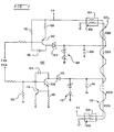
- Fig. 1 is a schematic diagram of a circuit for driving a two wire bus circuit.
- a bus driver circuit 100 of the present application is illustrated in schematic diagram form in Fig. 1.
- the driver circuit 100 is illustrated as driving a communications bus 102 comprising a twisted pair of wires which are terminated at least at one point to ground potential for one wire and to communications system signal potential +V for the other.
- the bus 102 is connected to the ground potential and the system signal potential +V through termination blocks 104 which each include a pair of resistors 106.
- One wire 102A of the bus 102 is terminated to system signal potential +V and is driven in response to a data signal TXA while the other wire 102B of the bus 102 is terminated to ground and is driven in response to a data signal TXB.
- the data signals TXA and TXB are opposite polarity signals which drive the two wires 102A and 102B of the bus 102 to opposite states, active and passive.
- the data signal TXA controls a first bus driver transistor 108 which inverts the data signal TXA and applies it to the wire 102A of the bus 102 through a Schottky diode 110.
- the wire 102A of the bus 102 is also connected to a pair of series connected zener diodes 112 which protects the driver circuit 100 from high transient voltages exceeding approximately forty-five (45) volts and a capacitor 114 which bypasses high frequency noise from the wire 102A to ground potential.
- the first bus driver transistor 108 sinks current from the bus 102 to ground, current flow through the transistor 108 must be limited in the event the bus 102 and particularly the wire 102A of the bus 102 is shorted to positive vehicle operating potential (+12 volts) or even to double positive vehicle operating potential (+24 volts) which can be encountered during attempts to jump-start a vehicle including the bus driver circuit 100.
- Current limiting for the transistor 108 is threefold. Initially, the transistor 108 is selected to having decreasing gain at high current levels and to be packaged in a high power dissipation package. For example a one-and-a-half (1 1/2) watt SOT-223, PZT3904 bipolar npn transistor is currently preferred for the transistor 108.
- the data signal TXB controls a second bus driver transistor 120 which inverts the data signal TXB and applies it to the wire 102B of the bus 102 through a Schottky diode 122.
- the wire 102B of the bus 102 is also connected to a pair of series connected zener diodes 124 which protects the driver circuit 100 from high transient voltages exceeding approximately forty-five (45) volts and a capacitor 126 which bypasses high frequency noise from the wire 102B to ground potential.
- the transistor 120 Current flow through the transistor 120 must be limited in the event the bus 102 and particularly the wire 102B of the bus 102 is shorted to ground potential. If the wire 102B of the bus 102 is shorted to operating potential (+12 volts) or even to double vehicle operating potential (+24 volts), the transistor 120 and hence the driver circuit 110 are protected by the Schottky diode 122 which is reverse biased for such conditions. Current limiting for the transistor 120 is twofold and, to some extent, threefold as with the transistor 108. Initially, the transistor 120 is selected to have decreasing gain at high current levels and is packaged in a high power dissipation package. For example a one-and-a-half (1 1/2) watt SOT-223, PZT3906 bipolar pnp transistor is currently preferred for the transistor 120.
- a resistor 128 which performs emitter degeneration for the transistor 120.
- a small amount of current limiting is also provided by a resistor 130 since current through the resistor 130 increases with increasing current flow through the transistor 120 and thereby reduces the base drive for the transistor 120.
- the primary reason for the resistor 130 is to prevent the transistor 120 from turning on if the input is open circuited or otherwise goes to a high impedance level.
- a resistor 132 serves a similar function for the transistor 108.
- Switch time control means comprising capacitors 134, 136 round the turn-on and turn-off edges of bus driver signals produced by the transistors 108, 120.
- the connections of the capacitors 134, 136 take advantage of the Miller effect to effectively increase their capacitance values. Accordingly, the capacitors 134, 136 reduce radiated emissions from the bus driver circuit 100.
- the capacitors 134, 136 also reduce the effect of mismatches between the bus driver transistors 108, 120.
- the capacitors 134, 136 reduce the radiated emissions generated by the bus driver circuit 100 which can result, for example, if the turn-off times of the transistors 108, 120 are mismatched.
- the Schottky diodes 110, 122 protect the bus driver circuit 100 and provide symmetry for driving the bus 102 while reducing the output level of bus signals by less than 0.4 volts.
- the Schottky diodes 110, 122 and the collector base junction of the transistor 108 also reduce the effective system bus capacitance by substantially isolating bus driver capacitance for nodes which are not trying to transmit. This isolation is important for large multiplex communications systems having from sixteen (16) to thirty two (32) nodes where all nodes do not try to transmit simultaneously. Isolation is also important for smaller systems which operate at high speed from 83.3 to 166.7 KBPS.
- bus driver circuit which can survive short circuits of a connected bus circuit to ground potential up to double vehicle operating potential without being disabled.
- the bus driver circuit prevents disabling of a bus circuit for loss of power or ground for one or a number of nodes connected to the bus.
- reliability and speed are enhanced by use of the bus driver circuit of the present invention.
Landscapes
- Engineering & Computer Science (AREA)
- General Engineering & Computer Science (AREA)
- Theoretical Computer Science (AREA)
- Computer Hardware Design (AREA)
- Physics & Mathematics (AREA)
- General Physics & Mathematics (AREA)
- Power Engineering (AREA)
- Small-Scale Networks (AREA)
Applications Claiming Priority (2)
| Application Number | Priority Date | Filing Date | Title |
|---|---|---|---|
| US41367 | 1993-04-01 | ||
| US08/041,367 US5311514A (en) | 1993-04-01 | 1993-04-01 | Driver for bus circuit of motor vehicle multiplex communications system |
Publications (3)
| Publication Number | Publication Date |
|---|---|
| EP0618681A2 true EP0618681A2 (de) | 1994-10-05 |
| EP0618681A3 EP0618681A3 (de) | 1995-12-06 |
| EP0618681B1 EP0618681B1 (de) | 1998-08-26 |
Family
ID=21916123
Family Applications (1)
| Application Number | Title | Priority Date | Filing Date |
|---|---|---|---|
| EP94301833A Expired - Lifetime EP0618681B1 (de) | 1993-04-01 | 1994-03-15 | Treiberschaltung für die Bus-Schaltung eines Kraftfahrzeug-Multiplex-Kommunikationssystems |
Country Status (4)
| Country | Link |
|---|---|
| US (1) | US5311514A (de) |
| EP (1) | EP0618681B1 (de) |
| DE (1) | DE69412680T2 (de) |
| ES (1) | ES2119962T3 (de) |
Cited By (3)
| Publication number | Priority date | Publication date | Assignee | Title |
|---|---|---|---|---|
| DE19647131A1 (de) * | 1996-11-14 | 1998-05-28 | Liebherr Werk Ehingen | Vorrichtung und Verfahren zur zeitmultiplexen Übertragung von Informationen |
| US6276485B1 (en) | 1998-12-30 | 2001-08-21 | Bt Industries Ab | Device at tiller truck |
| US6897639B2 (en) | 2001-09-19 | 2005-05-24 | Vega Grieshaber Kg | Circuit arrangement for the power supply of a two-wire sensor |
Families Citing this family (12)
| Publication number | Priority date | Publication date | Assignee | Title |
|---|---|---|---|---|
| US5471663A (en) * | 1993-07-01 | 1995-11-28 | Motorola, Inc. | Expanded microcomputer system for controlling radio frequency interference |
| US5959481A (en) * | 1997-02-18 | 1999-09-28 | Rambus Inc. | Bus driver circuit including a slew rate indicator circuit having a one shot circuit |
| US20070050095A1 (en) * | 2005-09-01 | 2007-03-01 | Polaris Industries Inc. | Controller area network based self-configuring vehicle management system and method |
| US7669682B2 (en) * | 2007-01-17 | 2010-03-02 | Polaris Industries Inc. | Rear suspension for a two wheeled vehicle |
| USD567715S1 (en) | 2007-01-17 | 2008-04-29 | Polaris Industries Inc. | Motorcycle |
| US7748746B2 (en) * | 2007-01-17 | 2010-07-06 | Polaris Industries Inc. | Fuel tank arrangement for a vehicle |
| US8994494B2 (en) * | 2008-10-10 | 2015-03-31 | Polaris Industries Inc. | Vehicle security system |
| US11209286B2 (en) | 2013-02-26 | 2021-12-28 | Polaris Industies Inc. | Recreational vehicle interactive telemetry, mapping and trip planning system |
| US9644969B2 (en) | 2013-02-26 | 2017-05-09 | Polaris Industries Inc. | Recreational vehicle interactive telemetry, mapping, and trip planning system |
| US9324195B2 (en) | 2013-02-26 | 2016-04-26 | Polaris Industries Inc. | Recreational vehicle interactive, telemetry, mapping, and trip planning system |
| CN108604320B (zh) | 2016-02-10 | 2022-09-23 | 北极星工业有限公司 | 休闲车辆组管理系统 |
| US11400997B2 (en) | 2016-05-23 | 2022-08-02 | Indian Motorcycle International, LLC | Display systems and methods for a recreational vehicle |
Family Cites Families (10)
| Publication number | Priority date | Publication date | Assignee | Title |
|---|---|---|---|---|
| US4337465A (en) * | 1980-09-25 | 1982-06-29 | Burroughs Corporation | Line driver circuit for a local area contention network |
| JPS5922414B2 (ja) * | 1980-10-08 | 1984-05-26 | 富士通株式会社 | ラインドライバ回路 |
| US4425564A (en) * | 1981-11-04 | 1984-01-10 | General Motors Corporation | Multiplex wiring system for motor vehicles |
| JPS61210738A (ja) * | 1985-03-14 | 1986-09-18 | Nissan Motor Co Ltd | 車両用信号通信装置 |
| FR2598871B1 (fr) * | 1986-05-14 | 1988-09-30 | Bendix Electronics Sa | Circuit d'interface bidirectionnel presentant un acces unipolaire et un acces bipolaire pour des signaux logiques |
| FR2623674B1 (fr) * | 1987-11-25 | 1990-04-20 | Peugeot | Dispositif de transmission d'informations pour vehicule automobile et procede de mise en oeuvre d'un tel dispositif |
| US4890010A (en) * | 1988-12-22 | 1989-12-26 | Ncr Corporation | Matched current source serial bus driver |
| US5077756A (en) * | 1990-05-31 | 1991-12-31 | Acculan Ltd. | Data network line driver |
| GB2248352A (en) * | 1990-09-25 | 1992-04-01 | Sun Microsystems Inc | Suppressing power transients in a computer system bus |
| DE4133764C1 (de) * | 1991-10-11 | 1993-02-18 | Texas Instruments Deutschland Gmbh, 8050 Freising, De |
-
1993
- 1993-04-01 US US08/041,367 patent/US5311514A/en not_active Expired - Lifetime
-
1994
- 1994-03-15 DE DE69412680T patent/DE69412680T2/de not_active Expired - Fee Related
- 1994-03-15 ES ES94301833T patent/ES2119962T3/es not_active Expired - Lifetime
- 1994-03-15 EP EP94301833A patent/EP0618681B1/de not_active Expired - Lifetime
Cited By (4)
| Publication number | Priority date | Publication date | Assignee | Title |
|---|---|---|---|---|
| DE19647131A1 (de) * | 1996-11-14 | 1998-05-28 | Liebherr Werk Ehingen | Vorrichtung und Verfahren zur zeitmultiplexen Übertragung von Informationen |
| DE19647131C2 (de) * | 1996-11-14 | 2001-12-06 | Liebherr Werk Ehingen | Vorrichtung und Verfahren zur zeitmultiplexen Übertragung von Informationen |
| US6276485B1 (en) | 1998-12-30 | 2001-08-21 | Bt Industries Ab | Device at tiller truck |
| US6897639B2 (en) | 2001-09-19 | 2005-05-24 | Vega Grieshaber Kg | Circuit arrangement for the power supply of a two-wire sensor |
Also Published As
| Publication number | Publication date |
|---|---|
| ES2119962T3 (es) | 1998-10-16 |
| EP0618681A3 (de) | 1995-12-06 |
| DE69412680T2 (de) | 1999-01-14 |
| DE69412680D1 (de) | 1998-10-01 |
| US5311514A (en) | 1994-05-10 |
| EP0618681B1 (de) | 1998-08-26 |
Similar Documents
| Publication | Publication Date | Title |
|---|---|---|
| EP0618681B1 (de) | Treiberschaltung für die Bus-Schaltung eines Kraftfahrzeug-Multiplex-Kommunikationssystems | |
| US6324044B1 (en) | Driver for controller area network | |
| US5617282A (en) | Data communication system | |
| US3911296A (en) | Capacitance multiplier circuit | |
| US5821796A (en) | Circuitry for providing a high impedance state when powering down a single port node | |
| US4005342A (en) | Integrated circuit overvoltage protection circuit | |
| US7218497B2 (en) | Protective circuit for protection against over-voltage for a CAN bus transceiver | |
| GB2233125A (en) | Alternator voltage transient minimisation. | |
| JP2002261241A (ja) | 静電気保護回路 | |
| US5034875A (en) | Voltage multiplier circuit | |
| US20210184562A1 (en) | Power module and level conversion circuit thereof | |
| JPH06209592A (ja) | 誘導性負荷を給電する回路構成 | |
| US3974404A (en) | Integrated circuit interface stage for high noise environment | |
| JPH027461A (ja) | 集積回路保護用回路装置 | |
| US5053643A (en) | Integrated circuit including output circuit having input logic controlled by output logic | |
| US5047662A (en) | Inductive load driving circuit with inductively induced voltage compensating means | |
| GB2302466A (en) | Latching arrangement for switch in which the switch is turned off in response to a fault | |
| US5444400A (en) | Logic output circuit with high transient pull-up current | |
| US4945358A (en) | Short circuit protection arrangement for a driver circuit | |
| US5737165A (en) | Apparatus for databus fault isolation | |
| US6211694B1 (en) | Bus driver having noise removing circuit | |
| JP3341553B2 (ja) | 電力用半導体素子ゲート駆動回路用の信号伝送回路 | |
| EP0408124B1 (de) | Schutzschaltung gegen negative Überspannungen über der Stromversorgung einer integrierten Schaltung mit einer Leistungseinrichtung und seinem Regelkreis | |
| JPH03222516A (ja) | 半導体装置 | |
| US6194951B1 (en) | Method and device for diving an integrated power output stage |
Legal Events
| Date | Code | Title | Description |
|---|---|---|---|
| PUAI | Public reference made under article 153(3) epc to a published international application that has entered the european phase |
Free format text: ORIGINAL CODE: 0009012 |
|
| AK | Designated contracting states |
Kind code of ref document: A2 Designated state(s): DE ES GB NL |
|
| PUAL | Search report despatched |
Free format text: ORIGINAL CODE: 0009013 |
|
| AK | Designated contracting states |
Kind code of ref document: A3 Designated state(s): DE ES GB NL |
|
| 17P | Request for examination filed |
Effective date: 19960603 |
|
| 17Q | First examination report despatched |
Effective date: 19970326 |
|
| GRAG | Despatch of communication of intention to grant |
Free format text: ORIGINAL CODE: EPIDOS AGRA |
|
| GRAG | Despatch of communication of intention to grant |
Free format text: ORIGINAL CODE: EPIDOS AGRA |
|
| GRAH | Despatch of communication of intention to grant a patent |
Free format text: ORIGINAL CODE: EPIDOS IGRA |
|
| GRAH | Despatch of communication of intention to grant a patent |
Free format text: ORIGINAL CODE: EPIDOS IGRA |
|
| GRAA | (expected) grant |
Free format text: ORIGINAL CODE: 0009210 |
|
| AK | Designated contracting states |
Kind code of ref document: B1 Designated state(s): DE ES GB NL |
|
| REF | Corresponds to: |
Ref document number: 69412680 Country of ref document: DE Date of ref document: 19981001 |
|
| REG | Reference to a national code |
Ref country code: ES Ref legal event code: FG2A Ref document number: 2119962 Country of ref document: ES Kind code of ref document: T3 |
|
| REG | Reference to a national code |
Ref country code: GB Ref legal event code: 746 Effective date: 19990216 |
|
| PLBE | No opposition filed within time limit |
Free format text: ORIGINAL CODE: 0009261 |
|
| STAA | Information on the status of an ep patent application or granted ep patent |
Free format text: STATUS: NO OPPOSITION FILED WITHIN TIME LIMIT |
|
| 26N | No opposition filed | ||
| REG | Reference to a national code |
Ref country code: GB Ref legal event code: IF02 |
|
| PGFP | Annual fee paid to national office [announced via postgrant information from national office to epo] |
Ref country code: NL Payment date: 20030228 Year of fee payment: 10 |
|
| PGFP | Annual fee paid to national office [announced via postgrant information from national office to epo] |
Ref country code: ES Payment date: 20030321 Year of fee payment: 10 |
|
| PG25 | Lapsed in a contracting state [announced via postgrant information from national office to epo] |
Ref country code: ES Free format text: LAPSE BECAUSE OF NON-PAYMENT OF DUE FEES Effective date: 20040316 |
|
| PG25 | Lapsed in a contracting state [announced via postgrant information from national office to epo] |
Ref country code: NL Free format text: LAPSE BECAUSE OF NON-PAYMENT OF DUE FEES Effective date: 20041001 |
|
| NLV4 | Nl: lapsed or anulled due to non-payment of the annual fee |
Effective date: 20041001 |
|
| PGFP | Annual fee paid to national office [announced via postgrant information from national office to epo] |
Ref country code: GB Payment date: 20050307 Year of fee payment: 12 |
|
| PGFP | Annual fee paid to national office [announced via postgrant information from national office to epo] |
Ref country code: DE Payment date: 20050309 Year of fee payment: 12 |
|
| REG | Reference to a national code |
Ref country code: ES Ref legal event code: FD2A Effective date: 20040316 |
|
| PG25 | Lapsed in a contracting state [announced via postgrant information from national office to epo] |
Ref country code: GB Free format text: LAPSE BECAUSE OF NON-PAYMENT OF DUE FEES Effective date: 20060315 |
|
| PG25 | Lapsed in a contracting state [announced via postgrant information from national office to epo] |
Ref country code: DE Free format text: LAPSE BECAUSE OF NON-PAYMENT OF DUE FEES Effective date: 20061003 |
|
| GBPC | Gb: european patent ceased through non-payment of renewal fee |
Effective date: 20060315 |