EP0619613A2 - Heteroübergang-Bipolartransistor - Google Patents
Heteroübergang-Bipolartransistor Download PDFInfo
- Publication number
- EP0619613A2 EP0619613A2 EP94302456A EP94302456A EP0619613A2 EP 0619613 A2 EP0619613 A2 EP 0619613A2 EP 94302456 A EP94302456 A EP 94302456A EP 94302456 A EP94302456 A EP 94302456A EP 0619613 A2 EP0619613 A2 EP 0619613A2
- Authority
- EP
- European Patent Office
- Prior art keywords
- layer
- emitter
- base
- collector
- bipolar transistor
- Prior art date
- Legal status (The legal status is an assumption and is not a legal conclusion. Google has not performed a legal analysis and makes no representation as to the accuracy of the status listed.)
- Granted
Links
Images


Classifications
-
- H—ELECTRICITY
- H10—SEMICONDUCTOR DEVICES; ELECTRIC SOLID-STATE DEVICES NOT OTHERWISE PROVIDED FOR
- H10D—INORGANIC ELECTRIC SEMICONDUCTOR DEVICES
- H10D10/00—Bipolar junction transistors [BJT]
- H10D10/80—Heterojunction BJTs
- H10D10/821—Vertical heterojunction BJTs
Definitions
- the invention relates to a heterojunction bipolar transistor.
- it relates to a heterojunction bipolar transistor in which the material composition of the emitter-base heterojunction region is graded, thereby resulting in a high reliability.
- an AlGaAs/GaAs heterojunction bipolar transistor is formed using a semi-insulating GaAs substrate, doped GaAs base and collector layers and a doped AlGaAs emitter layer.
- the material composition of the emitter-base junction region is varied to achieve the desired electric potential barrier.
- the aluminum content is varied in the emitter-base junction region, namely a transition layer is provided between the emitter layer and base layer as shown by a broken line A in Figure 4.
- the aluminum content is varied as shown by a solid line B.
- a grading or abrupt emitter-base junction region refers to the emitter-base junction region which includes the emitter, transition and base layers and of which the composition is graded linearly, graded parabolically or changes abruptly.
- Fig. 5 shows a bipolar transistor having an emitter-base junction region in which the aluminum composition is graded linearly.
- the bipolar transistor of Fig. 5 has the following layers sequentially formed on a semi-insulating GaAs substrate 31: n+-GaAs layer 32, n-GaAs layer 33, p+-GaAs layer 34, n-Al X Ga 1-X As layer 35 (0 ⁇ X ⁇ 0.3), n-Al 0.3 Ga 0.7 As layer 36 and n+-GaAs layer 37.
- a collector electrode 38 is formed on n+-GaAs layer 32.
- a base electrode 39 is formed on p+-GaAs layer 34.
- An emitter electrode 40 is formed on n+-GaAs layer 37.
- Fig. 6 shows an energy band of the above described bipolar transistor of Fig. 5 in which the emitter-base junction region has a linearly graded aluminum composition.
- the bipolar transistor with the graded emitter-base junction region a barrier between the emitter and base is released owing to the emitter-base junction region of which the composition is graded linearly or parabolically. In that case, the injected electron density is varied in accordance with the change of applied emitter-base voltage.
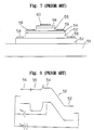
- Fig. 7 shows a bipolar transistor having an abrupt emitter-base junction region.
- the bipolar transistor of Fig. 7 has the following layers sequentially formed on a semi-insulating GaAs substrate 51: n+-GaAs layer 52, n-GaAs layer 53, p+-GaAs layer 54, n-Al 0.3 Ga 0.7 As layer 55 and n+-GaAs layer 56.
- a collector electrode 58 is formed on n+-GaAs layer 52.
- a base electrode 59 is formed on p+-GaAs layer 54.
- An emitter electrode 60 is formed on n+-GaAs layer 56.
- Fig. 8 shows an energy band of the above described bipolar transistor of Fig. 7 which has the abrupt emitter-base junction region.
- the bipolar transistor shown in this figure has an emitter-base junction region in which the aluminum composition is changed abruptly, so that electrons come into the base over a barrier from the emitter. In that case, the injected electron density is varied in accordance with the change of applied emitter-base voltage.
- the above described bipolar transistors with conventional grading or abrupt emitter-base junction region have carriers (i.e., electrons and holes) at a high density in the emitter-base junction region compared with the collector current density. Accordingly, the possibility of recombination of carriers (SHR recombination) which pass through the energy level of mid gap in this region is quite high. In particular, the possibility is very high at the semiconductor surface where a lot of energy levels exist.
- the electron concentration near the emitter-base junction region is generally quite high because the velocity at which the electrons are injected into the collector is low.
- the present invention provides a heterojunction bipolar transistor comprising a collector layer, a base layer, an emitter layer, a transition layer formed between the base layer and the emitter layer, a collector electrode connected to the collector layer, a base electrode connected to the base layer, and an emitter electrode connected to the emitter layer, wherein the emitter layer and the transition layer are formed of a composition including elements forming the base layer and at least one element different from the elements, a composition of the different element in the transition layer at the emitter side is substantially equal to that of the emitter layer, a composition of the different element in the transition layer at the base side is smaller than that of the emitter side and changes abruptly towards the base layer, and the composition of the transition layer varies in a continuous or discontinuous grading from the base side to the emitter side.
- the purpose of the present invention is to provide a heterojunction bipolar transistor in which the minority carrier concentrations in the emitter-base junction region are lowered to decrease the surface recombination current, whereby the reliability is hardly deteriorated by surface recombination.
- Fig. 1 is a schematic view in a cross section showing a main part of an embodiment of heterojunction bipolar transistor of the present invention.
- Fig. 2 is an energy band of the heterojunction bipolar transistor shown in Fig. 1.
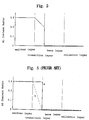
- Fig. 3 is a graph showing an aluminum composition in respective layers of the heterojunction bipolar transistor shown in Fig. 1.
- Fig. 4 is a graph showing an aluminum composition in respective layers of a conventional graded or abrupt heterojunction bipolar transistor.
- Fig. 5 is a schematic view in a cross section showing a main part of an embodiment of a conventional graded emitter-base junction heterojunction bipolar transistor.
- Fig. 6 is an energy band of the heterojunction bipolar transistor shown in Fig. 5.
- Fig. 7 is a schematic view in a cross section showing a main part of an embodiment of a conventional abrupt emitter-base junction heterojunction bipolar transistor.
- Fig. 8 is an energy band of the heterojunction bipolar transistor shown in Fig. 7.
- the heterojunction bipolar transistor of the present invention has at least a collector layer, a base layer, a transition layer and an emitter layer.
- the collector layer, base layer, transition layer, and emitter layer are formed on a semiconductor substrate.
- the substrate may be of a conventional type, for example a semiconductor substrate such as a silicon substrate and a compound semiconductor substrate formed of GaAs, InP, etc.
- the substrate itself can be used as the collector layer, in which case it is preferable that GaAs is used as the substrate and the other layers (such as the collector layer, base layer, transition layer and emitter layer) are formed thereon.
- a buffer layer, a contact layer or the like can also be formed (in addition to the collector, base, transition and emitter layers).
- An emitter electrode, base electrode and collector electrode are connected to the emitter layer, base layer and collector, respectively. If the emitter layer has an emitter contact layer thereon, the emitter electrode may be formed on the emitter contact layer. If the collector layer is formed on a subcollector layer, the collector is connected to the collector layer through the subcollector layer.
- a different element contained in the emitter and transition layers is an element different from those forming the base layer.
- the different element may form a compound semiconductor together with elements forming the collector, base, transition and emitter layers.
- the different element includes Al, In and the like doped in the GaAs compound semiconductor.
- the subcollector layer is formed by n+-GaAs and the collector layer are formed by n-GaAs.
- the impurities doped in the subcollector layer are n type impurities such as Si, Sn, Ge, S, Se and Te. These impurities are preferably doped in the subcollector layer at a concentration of 2 x 10¹⁸ to 8 x 1018 cm ⁇ 3 and in the collector layer preferably at 5 x 1016 cm ⁇ 3 to 1 x 1017 cm ⁇ 3.
- the preferred thicknesses for the subcollector layer and collector layers are about 0.5 to 1.0 ⁇ m and 0.4 to 1.0 ⁇ m, respectively.
- the base layer is formed on the collector layer.
- the base layer is preferably formed of p+-GaAs.
- the preferred impurity doped in the P-type base layer is an impurity such as C (carbon), Be, Zn; its concentration is 5 x 10¹⁸ to 5 x 1019 cm ⁇ 3; and the layer thickness is about 0.05 to 0.2 ⁇ m.
- the transition layer is formed on the base layer and the emitter layer is formed on the transition layer.
- the transition layer or emitter layer is formed of a composition including the same elements which forms the base layer and at least one element different from the elements forming the base layer.
- the composition of the different element is graded continuously or discontinuously from the base side to the emitter side.
- the different element on the base side of the transition layer is contained such that the composition thereof is abruptly changed between the transition layer and the base layer.
- the different element on the emitter side is contained at the same composition in the emitter layer.
- the transition layer is preferably AlXGa 1-X As.
- Y is in the range of about 0.2 to 0.5 and X is graded continuously or discontinuously in the range of about 0.1 to 0.5 from the base layer side to the emitter layer side.
- the value X on the base side is preferably in the range of 0.1 ⁇ X ⁇ 0.25 and X ⁇ Y-0.05 so as to cause an abrupt change in composition between the transition layer and the base layer.
- the composition between the transition layer and the base layer is graded in the manner that the gradation of the composition can not be distinguished from the continuous gradation. Therefore, it is not preferred. While, if X on the base side is greater than 0.25, the composition between the transition layer and the base layer is graded in an excessively abrupt manner, so that it is not preferred.
- X of the composition of the transition layer on the base side is preferably in the range of 0.1 ⁇ X ⁇ 0.15.
- the transition layer is characterized in that the composition is abruptly changed toward the base layer and is consistent with that of the emitter layer on the emitter side. It is preferred that the thickness of the transition layer is about 200 to 500 angstroms and the thickness of the emitter layer is about 0.1 to 0.2 ⁇ m.
- impurities to be doped in the emitter layer are n type impurities such as Si and Sn. The concentration of the impurity is preferably from 1 x 10¹⁷ to 2 x 1018 cm ⁇ 3.
- An emitter contact layer may be formed on the emitter layer. In that case, the emitter contact layer is preferably formed of n+-GaAs at an impurity concentration from 2 x 10¹⁸ to 8 x 1018 cm ⁇ 3 with a thickness of 0.1 to 0.4 ⁇ m.
- the respective layers of the transistor of the present invention can be epitaxially grown in sequence by a known method such as a metal organic chemical vapor deposition (MOCVD) and molecular beam epitaxial method (MBE).
- MOCVD metal organic chemical vapor deposition
- MBE molecular beam epitaxial method
- the emitter and emitter contact layers are etched by a known method to expose the base layer, then, the base and collector layers are etched to expose the subcollector layer.
- an emitter electrode, base electrode and collector electrode are formed on the emitter contact layer, base layer and subcollector layer, respectively.
- the materials of the electrodes general electrode materials may be used and are not specifically limited.
- AuGe/Ni/Au may be used for the collector and emitter electrodes and Ti/Pt/Au or Cr/Au may be used for the base electrode.
- a heat resisting metal including a refractory alloy such as WSi and WN for the emitter electrode, more preferably, WN is used.
- WN refractory alloy
- N+-InGaAs is preferably used for the emitter contact layer.
- the present invention can be applied to an NPN-type transistor as described above. It may be applied to a PNP-type transistor essentially in the same manner.
- GaAs and AlGaAs were used, but lattice match or lattice mismatch semiconductors such as InGaAs and InP can be also used.
- transistors having the heterojunction of which the composition is graded continuously or discontinuously as described above those having a heterojunction of which the composition is graded linearly as well as parabolically is also applicable.
- a low electron concentration in the emitter-base junction region is provided. This is because the step change in aluminum composition between the emitter and the base causes the electrons to be injected into the base at high velocity and because of the absence of any potential well in the conduction band of the emitter.
- the hole density in the emitter-base junction region is kept low because the relatively small abrupt compositional change at the emitter-base junction gives a low junction turn-on voltage for a given collector current.
- the low carrier densities in the emitter-base junction region keep the SHR recombination current at a low level.
- heterojunction bipolar transistor of the present invention examples are described below with reference to the figures.
- n+-GaAs subcollector layer 2 n-GaAs collector layer 3, p+-GaAs base layer 4, n-Al X Ga 1-X As transition layer 5, n-Al 0.3 Ga 0.7 As emitter layer 6 and n+-GaAs emitter contact layer 7 are sequentially formed on a semi-insulating GaAs substrate 1, a collector electrode 8 is formed on the n+-GaAs subcollector layer 2 as an ohmic electrode, a base electrode 9 is formed on p+-GaAs base layer 4 and an emitter electrode 10 is formed on n+-GaAs emitter contact layer 7.
- the n+-GaAs subcollector layer 2 is formed with a thickness of about 5,000 angstroms and doped with Si at a concentration of 5 x 1018 cm ⁇ 3.
- the n-GaAs collector layer 3 is formed with a thickness of about 5,000 angstroms and doped with Si at a concentration of 5 x 1016 cm ⁇ 3.
- the p+-GaAs base layer 4 is formed with a thickness of about 700 angstroms and doped with C at a concentration of 4 x 1019 cm ⁇ 3.
- the n-Al X Ga 1-X As transition layer 5 is formed with a thickness of about 200 angstroms and doped with Si at a concentration of 5 x 1017 cm ⁇ 3, where X is graded linearly from 0.2 to 0.3 from the side of p+-GaAs base layer 4 to the side of n+-Al 0.3 Ga 0.7 As emitter layer 6.
- the n+-Al 0.3 Ga 0.7 As emitter layer 6 is formed with a thickness of about 800 angstroms and doped with Si at a concentration of 5 x 1017 cm ⁇ 3.
- the n+-GaAs emitter contact layer 7 is formed with a thickness of about 1,000 angstroms and doped with Si at a concentration of 5 x 1018 cm ⁇ 3.
- the collector electrode 8 and emitter electrode 10 are formed of AuGe/Ni/Au and the base electrode 9 is formed of Ti/Pt/Au.
- the n+-GaAs subcollector layer 2, n-GaAs collector layer 3, p+-GaAs base layer 4, n-Al X Ga 1-X As transition layer 5, n+-Al 0.3 Ga 0.7 As emitter layer 6 and n+-GaAs emitter contact layer 7 are sequentially formed on the semi-insulating GaAs substrate 1.
- n-Al X Ga 1-X As transition layer 5 n+-Al 0.3 Ga 0.7 As emitter layer 6 and n+-GaAs emitter contact layer 7 are etched to expose the base layer.
- n-GaAs collector layer 3 and p+-GaAs base layer 4 are etched to form the layers in a desired shape.
- Fig. 3 shows the change of an aluminum composition in the respective layers of the above heterojunction bipolar transistor.
- the aluminum composition in the transition layer is equal to that of the emitter layer, 0.3, on the emitter side, and varies linearly towards the base layer from 0.3 to 0.2 of Al content and abruptly at the interface between the transition layer and the base layer.
- the emitter electrode is formed of WN and the emitter contact layer 7 is formed of N+-InGaAs, and doped with Si at the concentration of 1 x 10¹⁹ to 3 x 10 19 cm ⁇ 3.
- the conventional bipolar transistor is the same structure except for the structure corresponding to the transition layer of the invention. TABLE 1 250 hours 500 hours 1000 hours Example 0 % 20 % 30 % Bipolar transistor w/conventional grading structure 50 % 60 % 70 % Bipolar transistor w/conventional abrupt structure 40 % 50 % 70 %
- the transistor of the present invention has an extremely high reliability.
- the heterojunction bipolar transistor of the present invention comprising a collector layer, a base layer, an emitter layer, a transition layer formed between the base layer and the emitter, a collector electrode connected to the collector layer, a base electrode connected to the base layer, and an emitter electrode connected to the emitter layer, wherein the emitter layer and the transition layer are formed of a composition including elements forming the base layer and at least one element different from the elements, a composition of the different element in the transition layer at the emitter side is substantially equal to that of the emitter layer, a composition of the different element in the transition layer at the base side is smaller than that of the emitter side and varies abruptly towards the base layer, and the composition of the transition layer varies in a continuous or discontinuous grading from the base side to the emitter side, whereby a carrier density in the emitter-base junction region is lowered and SHR recombination current can be kept at a low level.
Landscapes
- Bipolar Transistors (AREA)
Applications Claiming Priority (3)
| Application Number | Priority Date | Filing Date | Title |
|---|---|---|---|
| JP8076093 | 1993-04-07 | ||
| JP08076093A JP3299807B2 (ja) | 1993-04-07 | 1993-04-07 | ヘテロ接合バイポーラトランジスタ |
| JP80760/93 | 1993-04-07 |
Publications (3)
| Publication Number | Publication Date |
|---|---|
| EP0619613A2 true EP0619613A2 (de) | 1994-10-12 |
| EP0619613A3 EP0619613A3 (de) | 1995-03-29 |
| EP0619613B1 EP0619613B1 (de) | 2001-11-21 |
Family
ID=13727378
Family Applications (1)
| Application Number | Title | Priority Date | Filing Date |
|---|---|---|---|
| EP94302456A Expired - Lifetime EP0619613B1 (de) | 1993-04-07 | 1994-04-07 | Heteroübergang-Bipolartransistor |
Country Status (4)
| Country | Link |
|---|---|
| US (1) | US5508536A (de) |
| EP (1) | EP0619613B1 (de) |
| JP (1) | JP3299807B2 (de) |
| DE (1) | DE69429127T2 (de) |
Cited By (4)
| Publication number | Priority date | Publication date | Assignee | Title |
|---|---|---|---|---|
| DE19718624A1 (de) * | 1997-05-02 | 1998-11-05 | Daimler Benz Ag | Heterobipolartransistor mit Mehrschicht-Emitterstruktur |
| US9882019B2 (en) | 2014-09-12 | 2018-01-30 | Qorvo Us, Inc. | Compound varactor |
| US10109623B2 (en) | 2014-05-08 | 2018-10-23 | Qorvo Us, Inc. | Dual-series varactor EPI |
| US10535784B2 (en) | 2014-05-08 | 2020-01-14 | Qorvo Us, Inc. | Dual stack varactor |
Families Citing this family (20)
| Publication number | Priority date | Publication date | Assignee | Title |
|---|---|---|---|---|
| US5981985A (en) * | 1996-06-24 | 1999-11-09 | The Trustees Of Columbia University In The City Of New York | Heterojunction bipolar transistor with buried selective sub-collector layer, and methods of manufacture |
| US5859447A (en) * | 1997-05-09 | 1999-01-12 | Yang; Edward S. | Heterojunction bipolar transistor having heterostructure ballasting emitter |
| JP3262056B2 (ja) | 1997-12-22 | 2002-03-04 | 日本電気株式会社 | バイポーラトランジスタとその製造方法 |
| JP3341740B2 (ja) | 1999-11-15 | 2002-11-05 | 日本電気株式会社 | ヘテロバイポーラ型トランジスタ及びその製造方法 |
| WO2002097864A2 (en) | 2001-05-30 | 2002-12-05 | Asm America, Inc | Low temperature load and bake |
| US6917061B2 (en) * | 2001-07-20 | 2005-07-12 | Microlink Devices, Inc. | AlGaAs or InGaP low turn-on voltage GaAs-based heterojunction bipolar transistor |
| US20050275056A1 (en) * | 2004-05-26 | 2005-12-15 | Stephen Forrest | Organic heterojunction bipolar transistor |
| US8278176B2 (en) | 2006-06-07 | 2012-10-02 | Asm America, Inc. | Selective epitaxial formation of semiconductor films |
| US7789965B2 (en) * | 2006-09-19 | 2010-09-07 | Asm Japan K.K. | Method of cleaning UV irradiation chamber |
| US20080289650A1 (en) * | 2007-05-24 | 2008-11-27 | Asm America, Inc. | Low-temperature cleaning of native oxide |
| US7759199B2 (en) * | 2007-09-19 | 2010-07-20 | Asm America, Inc. | Stressor for engineered strain on channel |
| US7871937B2 (en) | 2008-05-16 | 2011-01-18 | Asm America, Inc. | Process and apparatus for treating wafers |
| US8367528B2 (en) * | 2009-11-17 | 2013-02-05 | Asm America, Inc. | Cyclical epitaxial deposition and etch |
| US9885123B2 (en) | 2011-03-16 | 2018-02-06 | Asm America, Inc. | Rapid bake of semiconductor substrate with upper linear heating elements perpendicular to horizontal gas flow |
| US8809170B2 (en) | 2011-05-19 | 2014-08-19 | Asm America Inc. | High throughput cyclical epitaxial deposition and etch process |
| US9437772B2 (en) * | 2013-03-15 | 2016-09-06 | Matthew H. Kim | Method of manufacture of advanced heterojunction transistor and transistor laser |
| US11456374B2 (en) * | 2013-03-15 | 2022-09-27 | Matthew H. Kim | Germanium-silicon-tin (GeSiSn) heterojunction bipolar transistor devices |
| US9666702B2 (en) | 2013-03-15 | 2017-05-30 | Matthew H. Kim | Advanced heterojunction devices and methods of manufacturing advanced heterojunction devices |
| CN106683993A (zh) * | 2016-12-26 | 2017-05-17 | 厦门市三安光电科技有限公司 | 一种晶体管欧姆接触电极的制备方法 |
| CN114242825B (zh) * | 2021-11-12 | 2023-02-03 | 武汉敏芯半导体股份有限公司 | 侧面进光式背光监测光电探测器及其制作方法 |
Family Cites Families (5)
| Publication number | Priority date | Publication date | Assignee | Title |
|---|---|---|---|---|
| US4728616A (en) * | 1982-09-17 | 1988-03-01 | Cornell Research Foundation, Inc. | Ballistic heterojunction bipolar transistor |
| EP0106724B1 (de) * | 1982-09-17 | 1989-06-07 | ETAT FRANCAIS représenté par le Ministre des PTT (Centre National d'Etudes des Télécommunications) | Balistischer bipolarer Transistor mit Heteroübergängen |
| US4768074A (en) * | 1984-11-20 | 1988-08-30 | Kabushiki Kaisha Toshiba | Heterojunction bipolar transistor having an emitter region with a band gap greater than that of a base region |
| US5162243A (en) * | 1991-08-30 | 1992-11-10 | Trw Inc. | Method of producing high reliability heterojunction bipolar transistors |
| EP0562272A3 (en) * | 1992-03-23 | 1994-05-25 | Texas Instruments Inc | Microwave heterojunction bipolar transistors with emitters designed for high power applications and method for fabricating same |
-
1993
- 1993-04-07 JP JP08076093A patent/JP3299807B2/ja not_active Expired - Fee Related
-
1994
- 1994-04-07 DE DE69429127T patent/DE69429127T2/de not_active Expired - Fee Related
- 1994-04-07 EP EP94302456A patent/EP0619613B1/de not_active Expired - Lifetime
- 1994-04-07 US US08/224,650 patent/US5508536A/en not_active Expired - Lifetime
Cited By (5)
| Publication number | Priority date | Publication date | Assignee | Title |
|---|---|---|---|---|
| DE19718624A1 (de) * | 1997-05-02 | 1998-11-05 | Daimler Benz Ag | Heterobipolartransistor mit Mehrschicht-Emitterstruktur |
| US10109623B2 (en) | 2014-05-08 | 2018-10-23 | Qorvo Us, Inc. | Dual-series varactor EPI |
| US10535784B2 (en) | 2014-05-08 | 2020-01-14 | Qorvo Us, Inc. | Dual stack varactor |
| US10833071B2 (en) | 2014-05-08 | 2020-11-10 | Qorvo Us, Inc. | Dual-series varactor EPI |
| US9882019B2 (en) | 2014-09-12 | 2018-01-30 | Qorvo Us, Inc. | Compound varactor |
Also Published As
| Publication number | Publication date |
|---|---|
| EP0619613A3 (de) | 1995-03-29 |
| JP3299807B2 (ja) | 2002-07-08 |
| DE69429127D1 (de) | 2002-01-03 |
| US5508536A (en) | 1996-04-16 |
| JPH06295919A (ja) | 1994-10-21 |
| DE69429127T2 (de) | 2002-06-20 |
| EP0619613B1 (de) | 2001-11-21 |
Similar Documents
| Publication | Publication Date | Title |
|---|---|---|
| US5508536A (en) | Heterojunction bipolar transistor having low electron and hole concentrations in the emitter-base junction region | |
| US5903018A (en) | Bipolar transistor including a compound semiconductor | |
| US6399971B1 (en) | Semiconductor device and method for fabricating the same | |
| US6043520A (en) | III-V heterojunction bipolar transistor having a GaAs emitter ballast | |
| JP2801624B2 (ja) | ヘテロ接合バイポーラトランジスタ | |
| US5429957A (en) | Method of manufacturing an heterojunction bipolar transistor | |
| US5767540A (en) | Hetero-junction bipolar transistor having AlGaAsP emitter layer underneath a base electrode | |
| Su et al. | Double heterojunction GaAs/Al x Ga1− x As bipolar transistors prepared by molecular beam epitaxy | |
| EP0316139B1 (de) | Anordnung, die eine Sperrschichtstruktur mit resonantem Tunneleffekt aufweist | |
| JPH08250509A (ja) | ヘテロ接合バイポーラトランジスタ | |
| US6768141B2 (en) | Heterojunction bipolar transistor (HBT) having improved emitter-base grading structure | |
| US5814843A (en) | Heterojunction bipolar transistor having a graded-composition base region | |
| EP1662557B1 (de) | Bipolartransistor mit heteroübergang | |
| EP0229672B1 (de) | Bipolarer Heteroübergangstransistor mit einem Basisbereich aus Germanium | |
| JPH10154714A (ja) | 化合物半導体装置およびその製造方法 | |
| JP2003318184A (ja) | ヘテロ接合バイポーラトランジスタ及びこれを製造する方法 | |
| EP0384113A2 (de) | Bipolarer Heteroübergangs-Transistor mit einer mehrschichtigen Basis | |
| JP2980630B2 (ja) | 化合物半導体装置 | |
| JP4405060B2 (ja) | ヘテロ接合型バイポーラトランジスタ | |
| JP2557613B2 (ja) | ヘテロ接合バイポーラトランジスタ | |
| JP2004022835A (ja) | ヘテロ接合バイポーラトランジスタ用エピタキシャルウェハ及びヘテロ接合バイポーラトランジスタ | |
| JPH11330087A (ja) | ヘテロ接合バイポーラトランジスタ及びその製造方法 | |
| JP2001028373A (ja) | ヘテロ接合バイポーラトランジスタ | |
| JPH063805B2 (ja) | ヘテロ接合バイポ−ラトランジスタ | |
| JPH09162195A (ja) | ヘテロ接合バイポーラトランジスタ |
Legal Events
| Date | Code | Title | Description |
|---|---|---|---|
| PUAI | Public reference made under article 153(3) epc to a published international application that has entered the european phase |
Free format text: ORIGINAL CODE: 0009012 |
|
| AK | Designated contracting states |
Kind code of ref document: A2 Designated state(s): DE FR GB SE |
|
| PUAL | Search report despatched |
Free format text: ORIGINAL CODE: 0009013 |
|
| AK | Designated contracting states |
Kind code of ref document: A3 Designated state(s): DE FR GB SE |
|
| 17P | Request for examination filed |
Effective date: 19950616 |
|
| 17Q | First examination report despatched |
Effective date: 19960911 |
|
| GRAG | Despatch of communication of intention to grant |
Free format text: ORIGINAL CODE: EPIDOS AGRA |
|
| GRAG | Despatch of communication of intention to grant |
Free format text: ORIGINAL CODE: EPIDOS AGRA |
|
| GRAG | Despatch of communication of intention to grant |
Free format text: ORIGINAL CODE: EPIDOS AGRA |
|
| GRAH | Despatch of communication of intention to grant a patent |
Free format text: ORIGINAL CODE: EPIDOS IGRA |
|
| GRAH | Despatch of communication of intention to grant a patent |
Free format text: ORIGINAL CODE: EPIDOS IGRA |
|
| GRAH | Despatch of communication of intention to grant a patent |
Free format text: ORIGINAL CODE: EPIDOS IGRA |
|
| GRAA | (expected) grant |
Free format text: ORIGINAL CODE: 0009210 |
|
| AK | Designated contracting states |
Kind code of ref document: B1 Designated state(s): DE FR GB SE |
|
| REG | Reference to a national code |
Ref country code: GB Ref legal event code: IF02 |
|
| REF | Corresponds to: |
Ref document number: 69429127 Country of ref document: DE Date of ref document: 20020103 |
|
| PGFP | Annual fee paid to national office [announced via postgrant information from national office to epo] |
Ref country code: GB Payment date: 20020404 Year of fee payment: 9 |
|
| PGFP | Annual fee paid to national office [announced via postgrant information from national office to epo] |
Ref country code: SE Payment date: 20020405 Year of fee payment: 9 |
|
| PLBE | No opposition filed within time limit |
Free format text: ORIGINAL CODE: 0009261 |
|
| STAA | Information on the status of an ep patent application or granted ep patent |
Free format text: STATUS: NO OPPOSITION FILED WITHIN TIME LIMIT |
|
| 26N | No opposition filed | ||
| PG25 | Lapsed in a contracting state [announced via postgrant information from national office to epo] |
Ref country code: GB Free format text: LAPSE BECAUSE OF NON-PAYMENT OF DUE FEES Effective date: 20030407 |
|
| PG25 | Lapsed in a contracting state [announced via postgrant information from national office to epo] |
Ref country code: SE Free format text: LAPSE BECAUSE OF NON-PAYMENT OF DUE FEES Effective date: 20030408 |
|
| GBPC | Gb: european patent ceased through non-payment of renewal fee |
Effective date: 20030407 |
|
| EUG | Se: european patent has lapsed | ||
| PGFP | Annual fee paid to national office [announced via postgrant information from national office to epo] |
Ref country code: DE Payment date: 20070405 Year of fee payment: 14 |
|
| PGFP | Annual fee paid to national office [announced via postgrant information from national office to epo] |
Ref country code: FR Payment date: 20070411 Year of fee payment: 14 |
|
| PG25 | Lapsed in a contracting state [announced via postgrant information from national office to epo] |
Ref country code: DE Free format text: LAPSE BECAUSE OF NON-PAYMENT OF DUE FEES Effective date: 20081101 |
|
| REG | Reference to a national code |
Ref country code: FR Ref legal event code: ST Effective date: 20081231 |
|
| PG25 | Lapsed in a contracting state [announced via postgrant information from national office to epo] |
Ref country code: FR Free format text: LAPSE BECAUSE OF NON-PAYMENT OF DUE FEES Effective date: 20080430 |