EP0619920B1 - Integrierte schaltung - Google Patents
Integrierte schaltung Download PDFInfo
- Publication number
- EP0619920B1 EP0619920B1 EP93901655A EP93901655A EP0619920B1 EP 0619920 B1 EP0619920 B1 EP 0619920B1 EP 93901655 A EP93901655 A EP 93901655A EP 93901655 A EP93901655 A EP 93901655A EP 0619920 B1 EP0619920 B1 EP 0619920B1
- Authority
- EP
- European Patent Office
- Prior art keywords
- integrated circuit
- regions
- substrate
- circuit according
- transistors
- Prior art date
- Legal status (The legal status is an assumption and is not a legal conclusion. Google has not performed a legal analysis and makes no representation as to the accuracy of the status listed.)
- Expired - Lifetime
Links
Images




Classifications
-
- H—ELECTRICITY
- H10—SEMICONDUCTOR DEVICES; ELECTRIC SOLID-STATE DEVICES NOT OTHERWISE PROVIDED FOR
- H10D—INORGANIC ELECTRIC SEMICONDUCTOR DEVICES
- H10D84/00—Integrated devices formed in or on semiconductor substrates that comprise only semiconducting layers, e.g. on Si wafers or on GaAs-on-Si wafers
- H10D84/80—Integrated devices formed in or on semiconductor substrates that comprise only semiconducting layers, e.g. on Si wafers or on GaAs-on-Si wafers characterised by the integration of at least one component covered by groups H10D12/00 or H10D30/00, e.g. integration of IGFETs
- H10D84/82—Integrated devices formed in or on semiconductor substrates that comprise only semiconducting layers, e.g. on Si wafers or on GaAs-on-Si wafers characterised by the integration of at least one component covered by groups H10D12/00 or H10D30/00, e.g. integration of IGFETs of only field-effect components
- H10D84/83—Integrated devices formed in or on semiconductor substrates that comprise only semiconducting layers, e.g. on Si wafers or on GaAs-on-Si wafers characterised by the integration of at least one component covered by groups H10D12/00 or H10D30/00, e.g. integration of IGFETs of only field-effect components of only insulated-gate FETs [IGFET]
- H10D84/85—Complementary IGFETs, e.g. CMOS
- H10D84/856—Complementary IGFETs, e.g. CMOS the complementary IGFETs having different architectures than each other, e.g. high-voltage and low-voltage CMOS
Definitions
- the invention relates to an integrated circuit with at least two active components, such as Transistors.
- Such integrated circuits are generally known and are currently in various "MOS” and / or bipolar technologies in large quantities manufactured.
- the structures of the circuits are currently being tried to further reduce, on the one hand, the packing density and on the other hand to increase the clock frequency.
- US-A-5 065 216 discloses a semiconductor integrated circuit described that from a substrate there is a conductive layer on the back Surface of the substrate and several Semiconductor layers on the front surface of the substrate. Very special conductive paths are provided with which supply voltages of the back of the circuit to the active elements can be performed.
- US-A-4 631 570 discloses an integrated circuit discloses the hidden oxide insulation and a Low resistance substrate discloses that is suitable to connect power supplies.
- the invention has for its object an integrated Circuit with at least two active components to indicate at which large packing densities minimized contact and crosstalk problems are.
- This training according to the invention can highest packing density with minimal process complexity to reach. Because of the simplicity and the planarity the construction of the circuit according to the invention Yield optimized and manufacturing costs minimized.
- the training according to the invention an optimization of gain and bandwidth.
- the lateral isolation areas can also pass through blocked p / n junctions or by dielectric Insulation layers are formed (claim 5).
- the lateral isolation areas are roughly hollow cylindrical Oxide areas exist that are made with material of Conductivity type of the highly conductive substrate filled are on which an insulating cover layer and in particular a silicon oxide layer is applied.
- FIG. 1 shows a first exemplary embodiment of an integrated circuit according to the invention with at least two active components, such as transistors.
- the circuit has a highly conductive substrate (1) which is connected to a pole of a supply voltage source.
- This highly conductive substrate (1) significantly reduces parasitic effects, namely crosstalk with higher packing density, fluctuations on the supply lines and aging problems on contacts.
- a highly doped "active" (preferably p + ) substrate (1) is used, which serves for current dissipation and as a fixed reference potential (ground).
- This "active" substrate offers a "half" additional wiring level.
- a substrate of another conductivity type can also be used.
- silicon wafers can be obtained inexpensively from disc manufacturers.
- the doping of this film is chosen so that N-channel transistors with optimal drift paths, N-channel transistors depletion type and suitable islands for arise for P-channel transistors.
- the film (2) is electrical with respect to the substrate (1) isolated.
- the film (2) is further divided into individual areas by lateral isolation areas.
- the lateral insulation is preferably carried out by dielectric insulation, in which a silicon core (4) is introduced into an oxide wall (3).
- nitride masking is preferably used as mask 1.
- Trench etching is typically carried out with reactive ion etching down to the depth of the p + substrate (1), the depth not being critical.
- the walls of the trenches are thermally oxidized and then the oxide base is removed, for example by directional reactive ion etching. This creates silicon seed areas from which silicon cores can be selectively grown in the epitaxial reactor, for example up to the height of the silicon surface. These surfaces are then thermally oxidized so that a field oxide (5) is formed which is almost coplanar with the surrounding silicon surfaces.
- p + deep diffusions are introduced using a mask 2. These lateral deep diffusion areas (6), which are introduced into the semiconducting layer, establish a conductive connection between the highly conductive substrate (1) and the corresponding areas of the layer (2).
- gate oxide is formed on all silicon islands thermally grown and typically polysilicon deposited as gate material.
- the polysilicon areas (7,8) are structured with a mask 3.
- a photoresist mask 4 exposes areas (9) into which a p-type ion implantation, for example with boron, takes place such that the polysilicon edges of the gates serve as masks for the transistors to be formed. These boron areas are diffused into a suitable depth. Now the entire area of the silicon wafer is implanted n + (eg with arsenic). This creates source and drain regions (10-12) of the NMOS transistors. A p + implantation (mask 5) connects the n + source, p-channel and sinker. There are now NMOS transistors of the so-called double-diffused type.
- the electrical channel length of these transistors is only determined by the difference in the diffusion depths of boron and arsenic, similar to the base width in NPN bipolar transistors.
- the fluctuations in these critical dimensions no longer have anything to do with fluctuations in the lithographic structuring, and transistors are obtained which have very small fluctuations in the electrical parameters in both microscopic and macroscopic areas of the silicon wafers.
- Double-diffused DMOS transistors are of the enhancement type (normally switched off). Your function can are understood as the series connection of an enhancement transistor with extremely short channel length (smaller as 0.3 ⁇ m in series with an N-type drift path, which also from the gate above into strong Electron accumulation is turned on.
- This type of transistor is characterized in that with the very short enhancement channel a very steep slope, or a very large current is produced, and that the following drift distance potential influences from the drain minimizes the source-side control path, so that a very low channel length modulation and therefore optimal high internal voltage gain of this transistor is achieved.
- the one with a given drain voltage (e.g. supply voltage 5V) over the drift path distributed field strength is so reduced that problems with are called charge carriers and corresponding transistor degradations be prevented.
- this type of MIS transistor has the highest possible Gain bandwidth or switching speed.
- NMOS transistor with the gate (8) was created by the Depletion type, i.e. is normally conductive.
- This Transistor is as a gate controlled resistor and therefore suitable as a load element. Its electrical channel length corresponds to the geometric width of the polysilicon gate, which are suitable for corresponding circuits is to be interpreted.
- a particularly advantageous design for the DMOS transistors consists of the gate, drain and possibly lateral isolation concentric or practically hexagonal, be arranged around source and sinker areas.
- the intermediate oxide is subsequently applied to a wafer surface that is only due to the polysilicon structures has a height profile.
- the conformity this oxide can thus be produced cheaply. This also facilitates the structuring of the Contact holes in this insulator film (mask 6).
- the low surface structure also has a favorable effect for the following films metal 1 (mask 7), intermediate oxide with vias (mask 8) and metal 2 (mask 9) out.
- FIG. 2 An integrated circuit according to the invention (also as SUPER-MOS technology) with complementary DMOS transistors are shown in FIG. 2.
- a p-region is required for a p-channel DMOS transistor (18) with a mask 10 in front of the formation of the poly areas.
- a submicron high performance can be complementary DMOS technology can be manufactured with only 12 masks (11 masks with junction isolation).
- Transistors with symmetrical base or channel areas for use in transmission gates, for elevation the transistor density and to save masks can be produced according to FIG. 3.
- a high packing density can be found in the complementary circuits can be achieved in that the complementary Drain areas at common circuit nodes directly side by side without lateral isolation can be (Fig. 4).
- the lateral isolation with trench enables the highest Packing density. Sated of this can also be a P + area be used simultaneously with the sinker (6) is generated (Fig. 5). Trench etching, wall oxidation and filling the trenches with silicon is not necessary.
- a three-layer metallization has the advantage that third metal (25) over the entire area for the positive supply voltage, for the dissipation of power loss, for EM shielding and to reduce crosstalk can be used.
- FIG. 6 shows a further exemplary embodiment of the invention, in which the integrated circuit is implemented on a direct bonding substrate.
- two wafers with an oxide surface (24) are "directly bonded".
- Commercial wafers (1) with p + or n + doping are used for this purpose.
- the upper wafer 82) has n-epidoping.
- the upper silicon layer is then removed except for the n-epidoping, so that a silicon layer with a thickness of 2 to 5 ⁇ m remains.
- the trench and the sinker generated. Trench etching with a mask is used for this 1; the oxide walls (3) are then doped. How in the embodiment shown in FIG. 1 the seed is opened with selective epitaxy (4) and the epitaxy autoxidized to a layer (5). The selective epitaxy also produces the sinker (6).
- mask 2 is used the gate oxidation (25) and the thin gate oxide (26). With A mask 3 is used to deposit and structure polysilicon.
- the p-tub is equipped with a Mask 4 as well as the channels (9, 20) and the source, Drain and bulk area (11, 21) generated with masks 5 to 8.
- the seed is used with a Mask 9 etched. Then there is a selective one Epitaxy step (area 27). With masks 10 to 13 the manufacturing process is completed.
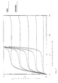
- Fig. 7 the Drain current as a function of drain voltage for a Component according to the invention (referred to as SUPERMOS) and a CMOS transistor is shown.
- FIG. 8 shows a further embodiment of an integrated circuit which also has an n + -diffused strip 42 in the p-doped substrate 1.
- the strip 42 is connected to the positive potential of the supply voltage U DD .
- the space charging zone which forms between the n + -doped region 42 and the p + -doped substrate serves as a barrier layer for these two potentials.
- the source region of so-called p-SuperMOS transistors is connected to the n + strips 42 via a corresponding sinker 39.
- This construction makes it possible to save the (often third) wiring layer on the surface of the circuit that was previously required for the supply voltage supply and to lay it in the silicon.
- the cables are now fed exclusively via silicon sections, which avoids heterogeneous material transitions, which have become a very critical part of highly integrated circuits as a result of aging.
- FIG. 9 shows an advantageous transistor arrangement, which also has a honeycomb-shaped power supply (dashed lines) with n + -doped interconnects for positive voltage supply.
- the positive supply voltage is abbreviated to U SS and the negative supply voltage to U DD .
- FIG. 1 A preferred transistor arrangement is shown in FIG which has a star-shaped transistor arrangement, with 45 ° rotated wiring direction. Since the Wiring against the transistor star rotated by 45 ° is a very short intracell line length and at the same time allows a data path structure.
- 11a and 11b show integrated circuit designs emerged, where a complementary Transistor mounted vertically above the first transistor is.
- the corresponding manufacturing sequence begins after the intermediate oxide (14). It becomes a spacer oxide (31) applied the island for one to be manufactured limited crystalline silicon thin film transistor.
- the oxide (14) is now at the drain region of the former Transistor etched a seed opening. From this Seed opening becomes crystalline with selective epitaxy Silicon grown up; advantageously with high p-type doping.
- the selective crystalline growing silicon sets its growth laterally across the transistor (7) and is finally replaced by the spacer oxide (31) continue to grow.
- the excess silicon growth is made by selective chemical-mechanical polishing Effect removed until the crystalline film plan fills the island within the spacer oxide (31).
- the epitaxial film (32) is overgrown advantageously p-doped. At the far end of the overgrowth now become the source and gate of a PDMOS transistor with the source region (34), the channel region (33), the advantageously two-stage gate oxide (35) and the gate (36).
- the source implantation (34) is also used to manufacture the drain area (37) used.
- the thin film PDMOS transistor thus manufactured can in any way from litigation be optimized here; Slope, on-resistance, Miller capacity, freedom from leakage currents, especially the bottom of the film.
Landscapes
- Metal-Oxide And Bipolar Metal-Oxide Semiconductor Integrated Circuits (AREA)
- Insulated Gate Type Field-Effect Transistor (AREA)
- Element Separation (AREA)
- Semiconductor Integrated Circuits (AREA)
- Stabilization Of Oscillater, Synchronisation, Frequency Synthesizers (AREA)
Description
- Fig. 1 bis 11
- verschiedene Ausführungsbeispiele der Erfindung.
- Maske 1
- Trench (4)
- Maske 2
- Sinker (6)
- Maske 3
- p-Driftstrecke (18)
- Maske 4
- Poly-Gates (7, 19)
- Maske 5
- P-Kanal und N+-Gebiete
- Maske 6
- N-Kanal und P+-Gebiete
- Maske 7
- Kontakte
- Maske 8
- Metall 1
- Maske 9
- VIA
- Maske 10
- Metall 2
Claims (13)
- Integrierte Schaltung mit wenigstens zwei Transistoren, wobeiein hochleitendes halbleitendes Substrat (1) eines ersten Dotierungstyps vorgesehen ist, das mit einem Pol einer Vorsorgungsspannungsquelle verbunden ist,über einer Hauptoberfläche des Substrats eine halbleitende Schicht (2) eines, dem ersten Typ entgegengesetzten zweiten Dotierungstyps aufgebracht ist, die gegenüber dem Substrat elektrisch isoliert ist, und die durch laterale Isolationsgebiete (3, 4, 5), die sich bis zum Substrat erstrecken, in einzelne Bereiche aufgeteilt ist,in jeden der Bereiche wenigstens ein Transistor mit einem n- oder p-Kanal eingebracht ist,Sinker-Bereiche (6) des ersten Dotierungstyps vorgesehen sind, die in die halbleitende Schicht (2) derart eingebracht sind, daß sie sich vom hochleitenden Substrat (1) bis zum jeweiligen halbleitenden Gebiet des Transistors erstrecken und eine direkte, örtlich leitende Verbindung zwischen dem hochleitenden Substrat (1) und den entsprechenden halbleitenden Gebieten der entsprechenden Transistoren zur Versorgungsspannungszuführung der Transistoren herstellen.
- Integrierte Schaltung nach Anspruch 1,
dadurch gekennzeichnet, daß das hochleitende Substrat (1) aus p+-Silizium besteht. - Integrierte Schaltung nach einem der Ansprüche 1 bis 2,
dadurch gekennzeichnet, daß die lateralen Isolationsgebiete durch gesperrte p/n-Übergänge gebildet werden. - Integrierte Schaltung nach einem der Ansprüche 1 bis 2,
dadurch gekennzeichnet, daß die lateralen Isolationsgebiete durch dielektrische Isolationsschichten gebildet werden. - Integrierte Schaltung nach Anspruch 4,
dadurch gekennzeichnet, daß die lateralen Isolationsgebiete aus in etwa hohlzylindrischen Oxidgebieten (3) bestehen, die mit Material des Leitfähigkeitstyps des hochleitenden Substrats (4) ausgefüllt sind, auf das eine isolierende Schicht (5) aufgebracht ist. - Integrierte Schaltung nach Anspruch 5,
dadurch gekennzeichnet, daß die Deckschicht eine Siliziumoxidschicht ist. - Integrierte Schaltung nach einem der Ansprüche 1 bis 6,
dadurch gekennzeichnet, daß das hochleitende Substrat mit dem negativen Pol einer Versorgungsspannungsquelle verbunden ist. - Integrierte Schaltung nach einem der Ansprüche 1 bis 7,
dadurch gekennzeichnet, daß in das hochleitende Substrat Bereiche entgegengesetzter Dotierung implementiert sind. - Integrierte Schaltung nach Anspruch 8,
dadurch gekennzeichnet, daß die Bereiche n+-diffundierte Streifen- oder wabenförmige Bereiche sind, die mit dem positiven Pol einer Versorgungsspannungsquellen verbunden sind. - Integrierte Schaltung nach einem der Ansprüche 8 oder 9,
dadurch gekennzeichnet, daß die aktiven Bauelemente über Tiefdiffusionen, sogenannte Sinker-Bereiche (39), mit dem hochdotierten Substrat bzw. mit den betreffenden Bereichen des Substrates elektrisch verbunden sind. - Integrierte Schaltung nach einem der Ansprüche 1 bis 10,
dadurch gekennzeichnet, daß eine Vielzahl von aktiven Bauelementem in Form von Transistoren gemäß einer sternförmigen Transistorenanordnung miteinander verschaltet sind. - Integrierte Schaltung nach einem der Ansprüche 1 bis 4,
dadurch gekennzeichnet, daß komplementär ausgeführte Transistoren, vertikal durch eine Isolationsschicht getrennt, über den Transistoren angeordnet sind. - Integrierte Schaltung nach einem der Ansprüche 5 bis 11,
dadurch gekennzeichnet, daß in den voneinander isolierten Bereichen komplementäre, d.h. n+-p-n-n+ NMOS- bzw. p+-n-p-p+ PMOS-Transistoren eingebracht sind.
Applications Claiming Priority (3)
| Application Number | Priority Date | Filing Date | Title |
|---|---|---|---|
| DE4143209 | 1991-12-30 | ||
| DE4143209A DE4143209A1 (de) | 1991-12-30 | 1991-12-30 | Integrierte schaltung |
| PCT/DE1992/001090 WO1993013547A2 (de) | 1991-12-30 | 1992-12-30 | Integrierte schaltung |
Publications (2)
| Publication Number | Publication Date |
|---|---|
| EP0619920A1 EP0619920A1 (de) | 1994-10-19 |
| EP0619920B1 true EP0619920B1 (de) | 1999-10-06 |
Family
ID=6448255
Family Applications (1)
| Application Number | Title | Priority Date | Filing Date |
|---|---|---|---|
| EP93901655A Expired - Lifetime EP0619920B1 (de) | 1991-12-30 | 1992-12-30 | Integrierte schaltung |
Country Status (7)
| Country | Link |
|---|---|
| US (1) | US5635753A (de) |
| EP (1) | EP0619920B1 (de) |
| JP (1) | JPH07506458A (de) |
| AT (1) | ATE185451T1 (de) |
| CA (1) | CA2127260A1 (de) |
| DE (2) | DE4143209A1 (de) |
| WO (1) | WO1993013547A2 (de) |
Families Citing this family (10)
| Publication number | Priority date | Publication date | Assignee | Title |
|---|---|---|---|---|
| DE4300986C2 (de) * | 1992-01-17 | 1999-08-26 | Mitsubishi Electric Corp | Halbleitervorrichtung zur Elementisolierung und Herstellungsverfahren derselben |
| JPH06342846A (ja) * | 1993-04-07 | 1994-12-13 | Mitsubishi Electric Corp | トレンチ分離構造を有する半導体装置およびその製造方法 |
| DE19801095B4 (de) * | 1998-01-14 | 2007-12-13 | Infineon Technologies Ag | Leistungs-MOSFET |
| US6862720B1 (en) | 1999-10-28 | 2005-03-01 | National Semiconductor Corporation | Interconnect exhibiting reduced parasitic capacitance variation |
| US6414367B1 (en) * | 1999-10-28 | 2002-07-02 | National Semiconductor Corporation | Interconnect exhibiting reduced parasitic capacitance variation |
| US6710424B2 (en) | 2001-09-21 | 2004-03-23 | Airip | RF chipset architecture |
| US20060071304A1 (en) * | 2004-09-29 | 2006-04-06 | International Business Machines Corporation | Structure and layout of a fet prime cell |
| IT1398204B1 (it) | 2010-02-16 | 2013-02-14 | St Microelectronics Srl | Sistema e metodo per eseguire il test elettrico di vie passanti nel silicio (tsv - through silicon vias). |
| US9966318B1 (en) * | 2017-01-31 | 2018-05-08 | Stmicroelectronics S.R.L. | System for electrical testing of through silicon vias (TSVs) |
| WO2026015880A1 (en) * | 2024-07-12 | 2026-01-15 | Psemi Corporation | Radio frequency integrated circuits using extended drain mosfets |
Citations (1)
| Publication number | Priority date | Publication date | Assignee | Title |
|---|---|---|---|---|
| CH493097A (de) * | 1968-02-23 | 1970-06-30 | Itt | Integrierte Festkörperschaltung mit lediglich zwei Elektrodenzuleitungen |
Family Cites Families (4)
| Publication number | Priority date | Publication date | Assignee | Title |
|---|---|---|---|---|
| JPS5994453A (ja) * | 1982-10-25 | 1984-05-31 | ゼネラル・エレクトリック・カンパニイ | オン抵抗を低減した高圧半導体デバイス |
| US4631570A (en) * | 1984-07-03 | 1986-12-23 | Motorola, Inc. | Integrated circuit having buried oxide isolation and low resistivity substrate for power supply interconnection |
| US4819052A (en) * | 1986-12-22 | 1989-04-04 | Texas Instruments Incorporated | Merged bipolar/CMOS technology using electrically active trench |
| JPH02210860A (ja) * | 1989-02-09 | 1990-08-22 | Fujitsu Ltd | 半導体集積回路装置 |
-
1991
- 1991-12-30 DE DE4143209A patent/DE4143209A1/de not_active Withdrawn
-
1992
- 1992-12-30 WO PCT/DE1992/001090 patent/WO1993013547A2/de not_active Ceased
- 1992-12-30 DE DE59209755T patent/DE59209755D1/de not_active Expired - Fee Related
- 1992-12-30 EP EP93901655A patent/EP0619920B1/de not_active Expired - Lifetime
- 1992-12-30 JP JP5511356A patent/JPH07506458A/ja active Pending
- 1992-12-30 AT AT93901655T patent/ATE185451T1/de not_active IP Right Cessation
- 1992-12-30 US US08/256,237 patent/US5635753A/en not_active Expired - Fee Related
- 1992-12-30 CA CA002127260A patent/CA2127260A1/en not_active Abandoned
Patent Citations (1)
| Publication number | Priority date | Publication date | Assignee | Title |
|---|---|---|---|---|
| CH493097A (de) * | 1968-02-23 | 1970-06-30 | Itt | Integrierte Festkörperschaltung mit lediglich zwei Elektrodenzuleitungen |
Non-Patent Citations (1)
| Title |
|---|
| T. OHNO et. al., Electronics Letters, vol. 25 (1989) no. 16, Stevenage, 1071-1072 * |
Also Published As
| Publication number | Publication date |
|---|---|
| DE59209755D1 (de) | 1999-11-11 |
| JPH07506458A (ja) | 1995-07-13 |
| ATE185451T1 (de) | 1999-10-15 |
| WO1993013547A3 (de) | 1993-08-05 |
| EP0619920A1 (de) | 1994-10-19 |
| CA2127260A1 (en) | 1993-07-08 |
| US5635753A (en) | 1997-06-03 |
| DE4143209A1 (de) | 1993-07-01 |
| WO1993013547A2 (de) | 1993-07-08 |
Similar Documents
| Publication | Publication Date | Title |
|---|---|---|
| DE102009049774B4 (de) | BiCMOS-Schaltungsanordnung | |
| DE69615458T2 (de) | Dünnfilmtransistor über einem isolierten Halbleitersubstrat und Verfahren zur Herstellung | |
| DE69728259T2 (de) | Siliciumkarbid-cmos und herstellungsverfahren | |
| DE69618285T2 (de) | Quasi-vertikaler DMOS in MOS- oder BICMOS-Verfahren mit hohem Wirkungsgrad | |
| DE102009010174B9 (de) | Verfahren zur Herstellung eines Halbleiterbauelements und Halbleiterbauelement | |
| DE4215708C2 (de) | SRAM und Verfahren zu dessen Herstellung | |
| DE10309997A1 (de) | Halbleiterbauelement mit Isolationsschichtstruktur und Herstellungsverfahren hierfür | |
| WO2004077571A1 (de) | Bipolartransistor mit verbessertem basis-emitter-übergang und verfahren zur herstellung | |
| DE2655400A1 (de) | Halbleitervorrichtung und verfahren zu ihrer herstellung | |
| DE4139490A1 (de) | Bicmos-vorrichtung und verfahren zur herstellung derselben | |
| DE102009000624A1 (de) | Asymmetrische segmentierte Kanaltransistoren | |
| DE4300986C2 (de) | Halbleitervorrichtung zur Elementisolierung und Herstellungsverfahren derselben | |
| DE102004060170A1 (de) | Halbleitervorrichtung und Verfahren zu ihrer Herstellung | |
| DE102008034158A1 (de) | Integrierte Schaltung mit einer Halbleiteranordnung in Dünnfilm-SOI-Technologie | |
| DE19525069C1 (de) | Verfahren zur Herstellung einer integrierten CMOS-Schaltung | |
| DE2739586C2 (de) | Statischer Inverter mit Isolierschicht-Feldeffekttransistoren und Verfahren zur Herstellung | |
| DE102005018378A1 (de) | Halbleitervorrichtung der Bauart mit dielektrischer Isolierung | |
| DE102018202836A1 (de) | Seitlich doppelt diffundierte Metalloxid-Halbleiter (LDMOS)-Vorrichtung auf einem vollständig verarmten Silizium-auf-Isolator (FDSOI), die eine hohe Eingangsspannung zulässt | |
| DE3855775T2 (de) | Integrierte Schaltung mit kombinierten komplementären bipolaren und MOS-Transistoren auf gemeinsamem Substrat und Verfahren zu ihrer Herstellung | |
| DE3034894A1 (de) | Halbleiteranordnung mit komplementaeren halbleiter-bauelementen und verfahren zu dessen herstellung | |
| DE4139039A1 (de) | Halbleitervorrichtung | |
| DE102013225362A1 (de) | Erhöhen der durchbruchsspannung einer metalloxidhalbleitereinrichtung | |
| WO1993013547A2 (de) | Integrierte schaltung | |
| DE19540665C2 (de) | Halbleiterbauelement und Verfahren zu dessen Herstellung | |
| DE102020133745A1 (de) | Integrierte schaltung mit pn-übergang und vertikal ausgerichtetem feldeffekttransistor und verfahren zur herstellung von selbigem |
Legal Events
| Date | Code | Title | Description |
|---|---|---|---|
| PUAI | Public reference made under article 153(3) epc to a published international application that has entered the european phase |
Free format text: ORIGINAL CODE: 0009012 |
|
| 17P | Request for examination filed |
Effective date: 19940719 |
|
| AK | Designated contracting states |
Kind code of ref document: A1 Designated state(s): AT BE CH DE DK ES FR GB GR IE IT LI LU MC NL PT SE |
|
| 17Q | First examination report despatched |
Effective date: 19961029 |
|
| GRAG | Despatch of communication of intention to grant |
Free format text: ORIGINAL CODE: EPIDOS AGRA |
|
| GRAG | Despatch of communication of intention to grant |
Free format text: ORIGINAL CODE: EPIDOS AGRA |
|
| GRAH | Despatch of communication of intention to grant a patent |
Free format text: ORIGINAL CODE: EPIDOS IGRA |
|
| GRAH | Despatch of communication of intention to grant a patent |
Free format text: ORIGINAL CODE: EPIDOS IGRA |
|
| GRAA | (expected) grant |
Free format text: ORIGINAL CODE: 0009210 |
|
| AK | Designated contracting states |
Kind code of ref document: B1 Designated state(s): AT BE CH DE DK ES FR GB GR IE IT LI LU MC NL PT SE |
|
| PG25 | Lapsed in a contracting state [announced via postgrant information from national office to epo] |
Ref country code: SE Free format text: THE PATENT HAS BEEN ANNULLED BY A DECISION OF A NATIONAL AUTHORITY Effective date: 19991006 Ref country code: NL Free format text: LAPSE BECAUSE OF FAILURE TO SUBMIT A TRANSLATION OF THE DESCRIPTION OR TO PAY THE FEE WITHIN THE PRESCRIBED TIME-LIMIT Effective date: 19991006 Ref country code: IT Free format text: LAPSE BECAUSE OF FAILURE TO SUBMIT A TRANSLATION OF THE DESCRIPTION OR TO PAY THE FEE WITHIN THE PRESCRIBED TIME-LIMIT;WARNING: LAPSES OF ITALIAN PATENTS WITH EFFECTIVE DATE BEFORE 2007 MAY HAVE OCCURRED AT ANY TIME BEFORE 2007. THE CORRECT EFFECTIVE DATE MAY BE DIFFERENT FROM THE ONE RECORDED. Effective date: 19991006 Ref country code: GR Free format text: LAPSE BECAUSE OF NON-PAYMENT OF DUE FEES Effective date: 19991006 Ref country code: ES Free format text: THE PATENT HAS BEEN ANNULLED BY A DECISION OF A NATIONAL AUTHORITY Effective date: 19991006 |
|
| REF | Corresponds to: |
Ref document number: 185451 Country of ref document: AT Date of ref document: 19991015 Kind code of ref document: T |
|
| REG | Reference to a national code |
Ref country code: CH Ref legal event code: EP |
|
| REF | Corresponds to: |
Ref document number: 59209755 Country of ref document: DE Date of ref document: 19991111 |
|
| GBT | Gb: translation of ep patent filed (gb section 77(6)(a)/1977) |
Effective date: 19991108 |
|
| PG25 | Lapsed in a contracting state [announced via postgrant information from national office to epo] |
Ref country code: LU Free format text: LAPSE BECAUSE OF NON-PAYMENT OF DUE FEES Effective date: 19991230 Ref country code: AT Free format text: LAPSE BECAUSE OF NON-PAYMENT OF DUE FEES Effective date: 19991230 |
|
| PG25 | Lapsed in a contracting state [announced via postgrant information from national office to epo] |
Ref country code: LI Free format text: LAPSE BECAUSE OF NON-PAYMENT OF DUE FEES Effective date: 19991231 Ref country code: CH Free format text: LAPSE BECAUSE OF NON-PAYMENT OF DUE FEES Effective date: 19991231 Ref country code: BE Free format text: LAPSE BECAUSE OF NON-PAYMENT OF DUE FEES Effective date: 19991231 |
|
| PG25 | Lapsed in a contracting state [announced via postgrant information from national office to epo] |
Ref country code: PT Free format text: LAPSE BECAUSE OF FAILURE TO SUBMIT A TRANSLATION OF THE DESCRIPTION OR TO PAY THE FEE WITHIN THE PRESCRIBED TIME-LIMIT Effective date: 20000106 Ref country code: DK Free format text: LAPSE BECAUSE OF FAILURE TO SUBMIT A TRANSLATION OF THE DESCRIPTION OR TO PAY THE FEE WITHIN THE PRESCRIBED TIME-LIMIT Effective date: 20000106 |
|
| ET | Fr: translation filed | ||
| REG | Reference to a national code |
Ref country code: IE Ref legal event code: FG4D Free format text: GERMAN |
|
| NLV1 | Nl: lapsed or annulled due to failure to fulfill the requirements of art. 29p and 29m of the patents act | ||
| BERE | Be: lapsed |
Owner name: HOFFLINGER BERND Effective date: 19991231 |
|
| PG25 | Lapsed in a contracting state [announced via postgrant information from national office to epo] |
Ref country code: MC Free format text: LAPSE BECAUSE OF NON-PAYMENT OF DUE FEES Effective date: 20000630 |
|
| PLBE | No opposition filed within time limit |
Free format text: ORIGINAL CODE: 0009261 |
|
| STAA | Information on the status of an ep patent application or granted ep patent |
Free format text: STATUS: NO OPPOSITION FILED WITHIN TIME LIMIT |
|
| REG | Reference to a national code |
Ref country code: IE Ref legal event code: FD4D |
|
| 26N | No opposition filed | ||
| REG | Reference to a national code |
Ref country code: GB Ref legal event code: IF02 |
|
| PGFP | Annual fee paid to national office [announced via postgrant information from national office to epo] |
Ref country code: FR Payment date: 20021226 Year of fee payment: 11 |
|
| PGFP | Annual fee paid to national office [announced via postgrant information from national office to epo] |
Ref country code: GB Payment date: 20030321 Year of fee payment: 11 |
|
| PG25 | Lapsed in a contracting state [announced via postgrant information from national office to epo] |
Ref country code: GB Free format text: LAPSE BECAUSE OF NON-PAYMENT OF DUE FEES Effective date: 20031230 |
|
| GBPC | Gb: european patent ceased through non-payment of renewal fee |
Effective date: 20031230 |
|
| PG25 | Lapsed in a contracting state [announced via postgrant information from national office to epo] |
Ref country code: FR Free format text: LAPSE BECAUSE OF NON-PAYMENT OF DUE FEES Effective date: 20040831 |
|
| REG | Reference to a national code |
Ref country code: FR Ref legal event code: ST |
|
| PGFP | Annual fee paid to national office [announced via postgrant information from national office to epo] |
Ref country code: DE Payment date: 20050129 Year of fee payment: 13 |
|
| PG25 | Lapsed in a contracting state [announced via postgrant information from national office to epo] |
Ref country code: DE Free format text: LAPSE BECAUSE OF NON-PAYMENT OF DUE FEES Effective date: 20060701 |