EP0621484A1 - Verfahren und Gerät zum Anschliessen eines integrierten Schaltkreises an ein Testgerät - Google Patents
Verfahren und Gerät zum Anschliessen eines integrierten Schaltkreises an ein Testgerät Download PDFInfo
- Publication number
- EP0621484A1 EP0621484A1 EP94105123A EP94105123A EP0621484A1 EP 0621484 A1 EP0621484 A1 EP 0621484A1 EP 94105123 A EP94105123 A EP 94105123A EP 94105123 A EP94105123 A EP 94105123A EP 0621484 A1 EP0621484 A1 EP 0621484A1
- Authority
- EP
- European Patent Office
- Prior art keywords
- contactor
- semiconductor device
- leads
- contactor assembly
- test fixture
- Prior art date
- Legal status (The legal status is an assumption and is not a legal conclusion. Google has not performed a legal analysis and makes no representation as to the accuracy of the status listed.)
- Withdrawn
Links
- 239000004065 semiconductor Substances 0.000 title claims abstract description 70
- 238000000034 method Methods 0.000 title claims abstract description 17
- 230000008878 coupling Effects 0.000 title claims description 6
- 238000010168 coupling process Methods 0.000 title claims description 6
- 238000005859 coupling reaction Methods 0.000 title claims description 6
- 238000012360 testing method Methods 0.000 claims abstract description 65
- 230000013011 mating Effects 0.000 claims description 8
- 238000010998 test method Methods 0.000 claims description 3
- 230000005540 biological transmission Effects 0.000 description 3
- 239000000463 material Substances 0.000 description 3
- 230000032258 transport Effects 0.000 description 3
- KDLHZDBZIXYQEI-UHFFFAOYSA-N Palladium Chemical compound [Pd] KDLHZDBZIXYQEI-UHFFFAOYSA-N 0.000 description 2
- 230000000712 assembly Effects 0.000 description 2
- 238000000429 assembly Methods 0.000 description 2
- 238000005452 bending Methods 0.000 description 2
- DMFGNRRURHSENX-UHFFFAOYSA-N beryllium copper Chemical compound [Be].[Cu] DMFGNRRURHSENX-UHFFFAOYSA-N 0.000 description 2
- 230000007423 decrease Effects 0.000 description 2
- 230000003028 elevating effect Effects 0.000 description 2
- 238000004519 manufacturing process Methods 0.000 description 2
- BASFCYQUMIYNBI-UHFFFAOYSA-N platinum Chemical compound [Pt] BASFCYQUMIYNBI-UHFFFAOYSA-N 0.000 description 2
- 238000009966 trimming Methods 0.000 description 2
- RYGMFSIKBFXOCR-UHFFFAOYSA-N Copper Chemical compound [Cu] RYGMFSIKBFXOCR-UHFFFAOYSA-N 0.000 description 1
- BQCADISMDOOEFD-UHFFFAOYSA-N Silver Chemical compound [Ag] BQCADISMDOOEFD-UHFFFAOYSA-N 0.000 description 1
- HCHKCACWOHOZIP-UHFFFAOYSA-N Zinc Chemical compound [Zn] HCHKCACWOHOZIP-UHFFFAOYSA-N 0.000 description 1
- 239000000853 adhesive Substances 0.000 description 1
- 230000001070 adhesive effect Effects 0.000 description 1
- 239000000969 carrier Substances 0.000 description 1
- 150000001875 compounds Chemical class 0.000 description 1
- 239000004020 conductor Substances 0.000 description 1
- 229910052802 copper Inorganic materials 0.000 description 1
- 239000010949 copper Substances 0.000 description 1
- 230000009977 dual effect Effects 0.000 description 1
- 230000000694 effects Effects 0.000 description 1
- PCHJSUWPFVWCPO-UHFFFAOYSA-N gold Chemical compound [Au] PCHJSUWPFVWCPO-UHFFFAOYSA-N 0.000 description 1
- 229910052737 gold Inorganic materials 0.000 description 1
- 239000010931 gold Substances 0.000 description 1
- 230000000116 mitigating effect Effects 0.000 description 1
- 238000000465 moulding Methods 0.000 description 1
- 238000004806 packaging method and process Methods 0.000 description 1
- 229910052763 palladium Inorganic materials 0.000 description 1
- 229910052697 platinum Inorganic materials 0.000 description 1
- 229910000923 precious metal alloy Inorganic materials 0.000 description 1
- 238000002407 reforming Methods 0.000 description 1
- 229910052709 silver Inorganic materials 0.000 description 1
- 239000004332 silver Substances 0.000 description 1
- 239000007787 solid Substances 0.000 description 1
- 229910052725 zinc Inorganic materials 0.000 description 1
- 239000011701 zinc Substances 0.000 description 1
Images

Classifications
-
- G—PHYSICS
- G01—MEASURING; TESTING
- G01R—MEASURING ELECTRIC VARIABLES; MEASURING MAGNETIC VARIABLES
- G01R1/00—Details of instruments or arrangements of the types included in groups G01R5/00 - G01R13/00 and G01R31/00
- G01R1/02—General constructional details
- G01R1/04—Housings; Supporting members; Arrangements of terminals
- G01R1/0408—Test fixtures or contact fields; Connectors or connecting adaptors; Test clips; Test sockets
- G01R1/0433—Sockets for IC's or transistors
Definitions
- the present invention relates, in general, to testing semiconductor devices and, more particularly, to testing non-singulated semiconductor devices which are attached to a leadframe.
- semiconductor devices are usually placed in packages for protection from mechanical stresses.
- the steps used in packaging semiconductor devices generally include mounting a plurality of semiconductor devices to a leadframe, forming wire bonds between the semiconductor devices and the leadframe, and encapsulating the semiconductor devices within a molding compound. Subsequently, the leadframe is trimmed, formed, and separated, thereby producing individual or singulated packaged semiconductor devices.
- Semiconductor devices mounted to a leadframe may be electrically tested after the trimming step because they are electrically isolated from one another. However, most semiconductor device manufacturers do not test the packaged semiconductor devices until after they have been singulated. Electrically testing the packaged semiconductor devices prior to singulation is tricky because the leadframe leads are in a very fragile and vulnerable position and may, therefore, be easily damaged. Any damage to the leads amounts to destroying the packaged semiconductor device. The probability of damaging the leads is reduced by performing the steps of trimming, forming, and singulation sequentially using the same apparatus.
- the method should test the encapsulated semiconductor devices before the leads are "formed”. Further, it would be advantageous that the method reduce cycle time and testing costs. The method should also reduce the number of times the singulated packaged semiconductor devices are handled.
- the present invention provides a method and an apparatus for coupling a semiconductor device with a tester and subsequently testing the semiconductor device.
- a test fixture comprising a housing having at least one side.
- the at least one side includes a recess having a mouth and a backwall.
- At least two upper cantilever structures extend from an upper portion of the backwall and at least two lower cantilever structures extend from a lower portion of the backwall.
- the test fixture further includes a contactor assembly having at least one lead which is positioned between the at least two upper and lower cantilever structures when the contactor assembly is mounted to the housing.
- a method of testing semiconductor devices is provided by mating the test fixture to a tester. A non-singulated packaged semiconductor device is placed on the test fixture and electrically tested.
- FIG. 1 illustrates a cut-away exploded perspective view of an embodiment of a test fixture 10 for mating with leadframe leads in accordance with the present invention.
- Test fixture 10 includes a rectangular shaped electrically nonconductive housing or base 11 having a top surface 12, a bottom surface 13, and four side surfaces 14.
- a cavity or recess 17 extends from each side surface 14 into nonconductive housing 11 wherein each cavity 17 has a pair of sidewalls 15, a mouth 18, and a backwall 19.
- test fixture 10 is described as having a rectangular shape with four cavities 17, it shall be understood that the shape of test fixture 10 and the number of cavities 17 extending from side surface 14 are not limitations of the present invention. Moreover, the following description of cavity 17 applies to each side surface 14 having a cavity 17.
- Each pair of sidewalls 15 extends from a corresponding side surface 14 into nonconductive housing 11.
- the pair of sidewalls 15 are substantially parallel to one another, substantially perpendicular to the corresponding side surface 14 from which they extend, and are spaced apart from corners formed by the intersection of sidewalls 14.
- Each pair of sidewalls 15 is connected via backwall 19, wherein backwall 19 is substantially perpendicular to said pair of sidewalls 15 and substantially parallel to the corresponding side surface 14.
- a threaded screw hole 16 Between each pair of sidewalls 15 and said corners is a threaded screw hole 16.
- each cavity 17 has an upper plurality of protrusions 20 which form upper cantilever structures and a lower plurality of protrusions 21 which form lower cantilever structures.
- Cantilevers 20 and 21 are connected to and extend from an upper and a lower portion, respectively, of backwall 19 toward mouth 18. Further, they are substantially parallel to and spaced apart from one another, substantially perpendicular to backwall 19, and have approximately the same length and width. Although cantilevers 20 and 21 have approximately the same length and width, cantilever 20 is thicker than cantilever 21. The greater thickness of cantilever 20 is advantageous for contactor assembly 30 as will be explained subsequently.
- the length of cantilevers 20 and 21 is less than the distance that cavity 17 extends into nonconductive housing 11 such that cantilevers 20 and 21 do not extend past sides 14. Further, cantilevers 20 and 21 are vertically spaced apart thereby forming a gap 27 between them.
- Test fixture 10 has a detachable contactor assembly 30 which includes a case 29 having a top side, a bottom side, and a plurality of contactor leads 31 extending therefrom. Although only a single detachable contactor assembly 30 is shown in FIG. 1, it shall be understood that test fixture 10 may have more than one detachable contactor assembly.
- Each contactor lead 31 is a unitary lead having a first end which extends or projects from the top side and a second end which extends or projects from the bottom side of contactor assembly 30. The first end is adapted to mate with a leadframe lead extending from a packaged semiconductor device 44 (FIG. 2) and the second end is adapted to mate with conductive traces (36) or contact pads on a printed circuit board 35 (FIG.
- contactor leads 31 be molded in or through case 29.
- contactor assembly 30 may be a molded structure wherein contactor leads 31 are molded therein.
- Contactor leads 31 are illustrated in FIG. 1 as being elongated rectangular structures, however it shall be understood that contactor leads 31 may have any suitable shape including, for example, having an elongated cylindrical shape.
- contactor leads 31 are made from a resilient conductor material such as a precious metal alloy comprising palladium, platinum, gold, silver, copper, and zinc and sold under the trademark "PALINEY" by J. M. Ney, or beryllium copper, or the like.
- the number of contactor leads 31 and cantilevers 20 and 21 are selected in accordance with the package type in which the semiconductor device to be tested is encapsulated.
- four contactor assemblies 30 are used for a 44 pin plastic leaded chip carrier package (PLCC).
- PLCC plastic leaded chip carrier package
- Each contactor assembly 30 is mated with a cavity 17 such that case 29 is placed between the upper and lower cantilever structures 20 and 21, respectively. Further, there is a cavity 17 present at each of the side surfaces 14 of rectangular housing 11.
- each contactor assembly 30 has twenty-two contactor leads 31 that are divided into eleven pairs wherein each pair is comprised of two contactor leads 31 that are side by side and abut one another.
- each pair of contactor leads 31 contacts a single pin or leadframe lead of a packaged semiconductor device.
- the use of two contactor leads 31 per semiconductor leadframe lead provides redundancy and increases the probability of a solid electrical connection between contactor leads 31 and the semiconductor leadframe leads.
- contactor assembly 30 is mated with housing 11 by inserting contactor assembly 30 into gap 27 such that the first ends of contactor leads 31 extend between upper cantilever structures 20 and the second ends of contactor leads 31 extend between lower cantilever structures 21.
- contactor leads 31 cooperate with cantilever structures 20 and 21 such that the first ends of contactor leads 31 become interdigitated with upper cantilever structures 20 and the second ends of contactor leads 31 become interdigitated with lower cantilever structures 21.
- Cantilevers 20 and 21 are also referred to as guidemembers. Making upper cantilever structure 20 thicker than lower cantilever structure 21 allows forming the first ends of contactor leads 31 with sufficient length to promote better contact between contactor leads 31 and leadframe leads (not shown). Further, the longer first ends permit additional play in contactor leads 31, which allows bending or reforming the first ends as they become worn, thereby increasing the life of contactor leads 31.
- Securing means 32 includes a stop (reference numeral 50 of FIG. 2) extending therefrom which is inserted into gap 27 and presses against contactor assembly 30 thereby securing contactor assembly 30 in place.
- Other ways of fastening retainer 32 to nonconductive housing 11 are well known to those skilled in the art and include clips, snaps, adhesive materials, or the like.
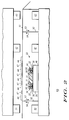
- test fixture 10 is shown in FIG. 1 with one side as an exploded perspective view, one side having a contactor assembly 30 secured to nonconductive housing 11 via securing means 32, and two sides without contactor assemblies 30.
- nonconductive housing 11 may have other features to facilitate the testing process such as, for example, a central aperture 36 for use with a sensor to indicate the presence of a packaged semiconductor device.
- nonconductive housing 11 includes contact block locating pins (not shown) which extend from the portion of holes 37 at bottom surface 13. Contact block locating pins serve to position test fixture 10 on loadboard 35 (FIG. 2).
- test fixture 10 includes leadframe locating pins 45 which position leadframes of non-singulated packaged semiconductor devices on test fixture 10. There may also be fastening holes 39 through which test fixture 10 is fastened or secured to a load board.
- FIG. 2 a highly simplified side view of a trim and form apparatus 40 having three tool sets is shown. Since several of the elements of test fixture 10 have been described with reference to FIG. 1, like numeral are used to designate identical or corresponding elements in FIG. 2. Further, FIG. 2 more clearly illustrates stop 50 extending from securing means 32. In addition, FIG. 2 illustrates test fixture 10 mounted to loadboard 35 and the mounting of the second ends of contactor leads 31 to conductive traces 36 of loadboard 35.
- a first tool set 41 provides lead trim and dam bar removal.
- a second tool set 42 is a forming tool set that forms the leads into a desired shape.
- a third tool set 43 is a singulating apparatus that separates each packaged semiconductor device into individual units.
- Trim and form apparatus are well known in the art.
- trim and form apparatus 40 is modified to have a tester 46 between first tool set 41 and second tool set 42.
- Trim and form apparatus 40 in conjunction with tester 46, serves as a means for electrically testing a packaged semiconductor device.
- Tester 46 includes a loadboard 35 having a plurality of conductive traces 36, wherein loadboard 35 may be attached to tester 46 with a set of screws (not shown). Other methods for attaching loadboard 35 to tester 46 include, for example, bonding, clipping, or clamping loadboard 35 to tester 46.
- Housing 11 is mounted to loadboard 35 of tester 46.
- tester 46 is shown in FIG. 2 as being mounted in trim and form apparatus 40, it shall be understood that FIG. 2 is a highly simplified representation of trim and form apparatus 40 and tester 46 and there are many other configurations for trim and form apparatus 40 and tester 46.
- tester 46 may be configured such that loadboard 35 is coupled to the test circuitry of tester 46 via a cable.
- loadboard 35 is mounted to trim and form apparatus 40, however the test circuitry to which loadboard 35 is coupled is located external to and detached from trim and form apparatus 40. Accordingly, the configuration of trim and form apparatus 40 and tester 46 is not a limitation of the present invention.
- a plurality of non-singulated packaged semiconductor devices 44 are transported into trim and form apparatus 40 via a transport track 51, wherein packaged semiconductor devices 44 are connected to each other by portions 47 of the leadframe.
- Packaged semiconductor devices 44 are transported to first tool set 41 wherein the leads are trimmed and the dam bar is removed.
- the plurality of semiconductor devices 44 are connected to one another by the leadframe portions 47, it shall be understood that they are electrically isolated from one another.
- trim and form apparatus 40 transports non-singulated packaged semiconductor devices 44 via transport track 51 to tester 46, and an elevating means 52 lowers a packaged semiconductor device 44 onto test fixture 10 (indicated by arrows 53).
- non-singulated packaged semiconductor device 44 is placed on test fixture 10 such that it is placed in contact with contactor assembly 30. More particularly, leadframe leads (not shown) are brought into contact with the first ends of contactor leads 31 and tester 46 tests the packaged semiconductor device 44 that is in contact with contactor leads 31.
- elevating means 52 raises non-singulated packaged semiconductor device 44 from test fixture 10 (indicated by arrows 54) and, if desired, another packaged semiconductor device 44 is placed on test fixture 10 and tested.
- packaged semiconductor devices 44 are transported to tool sets 42 and 43, for lead "forming" and singulation, respectively.
- the singulated devices have been tested prior to being released from trim and form apparatus 40.
- One advantage of the present invention is that the semiconductor devices are tested in the trim and form apparatus thereby reducing the number of times that the semiconductor devices must be handled; which in turn decreases the probability of damaging a packaged semiconductor device as well as decreases the cost of manufacturing packaged semiconductor devices.
- contactor leads 31 allows re-forming the contactor leads 31.
- the contactor leads 31 are of sufficient length and malleability to allow bending the leads to compensate for the length of the first end that becomes worn down by the abrasive wearing due to the testing of many semiconductor devices.
- the length and malleability of contactor leads 31 allow leads 31 to "scrub" the leadframe such that a good electrical contact is made therebetween.
- the length of the contactor leads 31 between the conductive traces on the loadboard and the bonding pads on the semiconductor device behave as a transmission line "stub". Since the contactor leads 31 contact the leadframe leads and the conductive traces 36 of the loadboard, the length of the transmission line "stub" is minimized.
- another advantage of the present invention is that the distance between the semiconductor die bonding pad and the loadboard is shortened, thereby mitigating any transmission line effects associated with high speed semiconductor device testing.
- the present invention is not limited to plastic leaded chip carriers, but applies to other package types such as, for example, dual in-line packages and quad flat packages. Further, the number of leads is not a limitation of the present invention. In other words, test fixtures in accordance with the present invention may be manufactured to accommodate packages having more or less than 44 leads.
- test fixture 10 of the present invention is not limited to testing non-singulated packaged semiconductor devices, but may be used for testing packaged semiconductor devices excised from the leadframe, i.e., singulated packaged semiconductor devices.
Landscapes
- Engineering & Computer Science (AREA)
- Computer Hardware Design (AREA)
- Microelectronics & Electronic Packaging (AREA)
- Physics & Mathematics (AREA)
- General Physics & Mathematics (AREA)
- Testing Of Individual Semiconductor Devices (AREA)
- Measuring Leads Or Probes (AREA)
- Testing Or Measuring Of Semiconductors Or The Like (AREA)
Applications Claiming Priority (2)
| Application Number | Priority Date | Filing Date | Title |
|---|---|---|---|
| US47901 | 1993-04-19 | ||
| US08/047,901 US5440231A (en) | 1993-04-19 | 1993-04-19 | Method and apparatus for coupling a semiconductor device with a tester |
Publications (1)
| Publication Number | Publication Date |
|---|---|
| EP0621484A1 true EP0621484A1 (de) | 1994-10-26 |
Family
ID=21951652
Family Applications (1)
| Application Number | Title | Priority Date | Filing Date |
|---|---|---|---|
| EP94105123A Withdrawn EP0621484A1 (de) | 1993-04-19 | 1994-03-31 | Verfahren und Gerät zum Anschliessen eines integrierten Schaltkreises an ein Testgerät |
Country Status (3)
| Country | Link |
|---|---|
| US (2) | US5440231A (de) |
| EP (1) | EP0621484A1 (de) |
| JP (1) | JPH0712893A (de) |
Cited By (1)
| Publication number | Priority date | Publication date | Assignee | Title |
|---|---|---|---|---|
| WO2017178105A1 (de) * | 2016-04-13 | 2017-10-19 | Rosenberger Hochfrequenztechnik Gmbh & Co. Kg | Kontaktstift und testsockel mit kontaktstiften |
Families Citing this family (21)
| Publication number | Priority date | Publication date | Assignee | Title |
|---|---|---|---|---|
| US6741085B1 (en) * | 1993-11-16 | 2004-05-25 | Formfactor, Inc. | Contact carriers (tiles) for populating larger substrates with spring contacts |
| US5777873A (en) * | 1996-04-29 | 1998-07-07 | Mitsubishi Semiconductor America, Inc. | Automated test fixture control system |
| US6690185B1 (en) | 1997-01-15 | 2004-02-10 | Formfactor, Inc. | Large contactor with multiple, aligned contactor units |
| US5956280A (en) * | 1998-03-02 | 1999-09-21 | Tanisys Technology, Inc. | Contact test method and system for memory testers |
| US6266342B1 (en) | 1998-04-08 | 2001-07-24 | Nortel Networks Limited | Adaption resource module and operating method therefor |
| JP3730428B2 (ja) * | 1998-12-22 | 2006-01-05 | 富士通株式会社 | 半導体装置試験用コンタクタの製造方法 |
| US6456099B1 (en) | 1998-12-31 | 2002-09-24 | Formfactor, Inc. | Special contact points for accessing internal circuitry of an integrated circuit |
| US7215131B1 (en) * | 1999-06-07 | 2007-05-08 | Formfactor, Inc. | Segmented contactor |
| US6259263B1 (en) | 1999-06-11 | 2001-07-10 | Micron Technology, Inc. | Compliant contactor for testing semiconductors |
| US6473702B1 (en) * | 2000-06-27 | 2002-10-29 | Advanced Micro Devices, Inc. | System and method for integrated singulation and inspection of semiconductor devices |
| US6690184B1 (en) | 2000-08-31 | 2004-02-10 | Micron Technology, Inc. | Air socket for testing integrated circuits |
| US7051427B2 (en) * | 2000-09-29 | 2006-05-30 | Texas Instruments Incorporated | Integrated circuit trimming device broken die sensor |
| US6617843B2 (en) * | 2001-01-15 | 2003-09-09 | Techwing Co., Ltd. | Contactor of the device for testing semiconductor device |
| US6783316B2 (en) * | 2001-06-26 | 2004-08-31 | Asm Assembly Automation Limited | Apparatus and method for testing semiconductor devices |
| US6729019B2 (en) | 2001-07-11 | 2004-05-04 | Formfactor, Inc. | Method of manufacturing a probe card |
| US6709877B2 (en) * | 2001-07-23 | 2004-03-23 | Asm Assembly Automation Limited | Apparatus and method for testing semiconductor devices |
| US6989295B1 (en) | 2002-01-09 | 2006-01-24 | Bridge Semiconductor Corporation | Method of making a semiconductor package device that includes an insulative housing with first and second housing portions |
| US6936495B1 (en) | 2002-01-09 | 2005-08-30 | Bridge Semiconductor Corporation | Method of making an optoelectronic semiconductor package device |
| US7190060B1 (en) | 2002-01-09 | 2007-03-13 | Bridge Semiconductor Corporation | Three-dimensional stacked semiconductor package device with bent and flat leads and method of making same |
| US6891276B1 (en) | 2002-01-09 | 2005-05-10 | Bridge Semiconductor Corporation | Semiconductor package device |
| US20050142345A1 (en) * | 2003-12-30 | 2005-06-30 | Saikumar Jayaraman | Curing processes for substrate imprinting, structures made thereby, and polymers used therefor |
Citations (4)
| Publication number | Priority date | Publication date | Assignee | Title |
|---|---|---|---|---|
| DE9004918U1 (de) * | 1989-05-19 | 1990-08-16 | Minnesota Mining And Mfg. Co., Saint Paul, Minn. | Fassung zum Einbrennen und Testen von TAB-Bauteilen |
| US5008615A (en) * | 1989-11-03 | 1991-04-16 | Motorola, Inc. | Means and method for testing integrated circuits attached to a leadframe |
| US5054188A (en) * | 1990-02-20 | 1991-10-08 | Micron Technology, Inc. | Trim cut and form machine |
| EP0458448A2 (de) * | 1990-05-24 | 1991-11-27 | Tektronix Inc. | Adapter und Prüfhalterung für einen Baustein mit integrierten Schaltungen |
Family Cites Families (12)
| Publication number | Priority date | Publication date | Assignee | Title |
|---|---|---|---|---|
| US4047780A (en) * | 1976-04-07 | 1977-09-13 | Cedrone Nicholas J | Test contactor system for semiconductor device handling apparatus |
| US4330683A (en) * | 1980-12-03 | 1982-05-18 | Bell Telephone Laboratories, Incorporated | Encapsulation for semiconductor device |
| JPS60101888A (ja) * | 1983-10-31 | 1985-06-05 | アンプ インコーポレーテッド | 電気コネクタ |
| US4866374A (en) * | 1984-10-12 | 1989-09-12 | Daymarc Corporation | Contactor assembly for testing integrated circuits |
| US4683423A (en) * | 1985-10-30 | 1987-07-28 | Precision Monolithics, Inc. | Leadless chip test socket |
| US4713611A (en) * | 1986-06-23 | 1987-12-15 | Vtc Incorporated | Burn-in apparatus for integrated circuits mounted on a carrier tape |
| US4839587A (en) * | 1988-03-29 | 1989-06-13 | Digital Equipment Corporation | Test fixture for tab circuits and devices |
| US4956605A (en) * | 1989-07-18 | 1990-09-11 | International Business Machines Corporation | Tab mounted chip burn-in apparatus |
| US5189363A (en) * | 1990-09-14 | 1993-02-23 | Ibm Corporation | Integrated circuit testing system having a cantilevered contact lead probe pattern mounted on a flexible tape for interconnecting an integrated circuit to a tester |
| US5086269A (en) * | 1991-03-08 | 1992-02-04 | Hewlett-Packard Company | Burn-in process and apparatus |
| US5177436A (en) * | 1991-05-21 | 1993-01-05 | Aseco Corporation | Contactor for testing integrated circuit chips mounted in molded carrier rings |
| US5226823A (en) * | 1992-01-09 | 1993-07-13 | Teledyne Kinectics | Indexing mechanism for precision alignment of electrical contacts |
-
1993
- 1993-04-19 US US08/047,901 patent/US5440231A/en not_active Expired - Fee Related
-
1994
- 1994-03-31 EP EP94105123A patent/EP0621484A1/de not_active Withdrawn
- 1994-04-12 JP JP6099323A patent/JPH0712893A/ja active Pending
-
1996
- 1996-12-02 US US08/759,324 patent/US5691650A/en not_active Expired - Fee Related
Patent Citations (4)
| Publication number | Priority date | Publication date | Assignee | Title |
|---|---|---|---|---|
| DE9004918U1 (de) * | 1989-05-19 | 1990-08-16 | Minnesota Mining And Mfg. Co., Saint Paul, Minn. | Fassung zum Einbrennen und Testen von TAB-Bauteilen |
| US5008615A (en) * | 1989-11-03 | 1991-04-16 | Motorola, Inc. | Means and method for testing integrated circuits attached to a leadframe |
| US5054188A (en) * | 1990-02-20 | 1991-10-08 | Micron Technology, Inc. | Trim cut and form machine |
| EP0458448A2 (de) * | 1990-05-24 | 1991-11-27 | Tektronix Inc. | Adapter und Prüfhalterung für einen Baustein mit integrierten Schaltungen |
Cited By (4)
| Publication number | Priority date | Publication date | Assignee | Title |
|---|---|---|---|---|
| WO2017178105A1 (de) * | 2016-04-13 | 2017-10-19 | Rosenberger Hochfrequenztechnik Gmbh & Co. Kg | Kontaktstift und testsockel mit kontaktstiften |
| CN109416374A (zh) * | 2016-04-13 | 2019-03-01 | 罗森伯格高频技术有限及两合公司 | 触针和具有触针的测试基座 |
| CN109416374B (zh) * | 2016-04-13 | 2020-02-04 | 罗森伯格高频技术有限及两合公司 | 触针和具有触针的测试基座 |
| US10641793B2 (en) | 2016-04-13 | 2020-05-05 | Rosenberger Hochfrequenztechnik Gmbh | Contact pin and test base having contact pins |
Also Published As
| Publication number | Publication date |
|---|---|
| US5440231A (en) | 1995-08-08 |
| US5691650A (en) | 1997-11-25 |
| JPH0712893A (ja) | 1995-01-17 |
Similar Documents
| Publication | Publication Date | Title |
|---|---|---|
| US5440231A (en) | Method and apparatus for coupling a semiconductor device with a tester | |
| KR100314135B1 (ko) | Bga 패키지의 전기적 검사를 위한 소켓 및 이를 이용한검사방법 | |
| US6407566B1 (en) | Test module for multi-chip module simulation testing of integrated circuit packages | |
| US5815000A (en) | Method for testing semiconductor dice with conventionally sized temporary packages | |
| US5600178A (en) | Semiconductor package having interdigitated leads | |
| IE53953B1 (en) | Packages for enclosing semiconductor elements | |
| JPH05196692A (ja) | 集積回路パッケージのテスト用のコネクタ・アセンブリ | |
| JP2016197120A (ja) | パッケージ化された半導体デバイスを試験するよう構成された高温セラミックソケット | |
| US5982186A (en) | Contactor for test applications including membrane carrier having contacts for an integrated circuit and pins connecting contacts to test board | |
| US3953101A (en) | Electrical connector assemblies | |
| KR101062643B1 (ko) | 전자 콤포넌트의 테스트 방법 | |
| JP2904193B2 (ja) | Icソケット | |
| JPH09304472A (ja) | 接続装置 | |
| KR940009571B1 (ko) | 번인소켓 | |
| JP2972634B2 (ja) | Icソケット | |
| US5242838A (en) | Method of manufacturing a semiconductor device | |
| JPH0590453A (ja) | 半導体装置の特性検査用ソケツト | |
| JPS62276861A (ja) | 半導体評価装置 | |
| JPH11118875A (ja) | バーンイン基板及びそれを用いたバーンイン方法 | |
| JP3172305B2 (ja) | 半導体装置の製造方法 | |
| KR950006471A (ko) | 테스트 소켓 및 그를 이용한 노운 굿 다이 제조방법 | |
| KR100190930B1 (ko) | 베어 다이의 테스트 지그 | |
| JP2710203B2 (ja) | Icソケット | |
| JPH03267772A (ja) | 接触子可動型icソケット | |
| JPH04162755A (ja) | Icソケット |
Legal Events
| Date | Code | Title | Description |
|---|---|---|---|
| PUAI | Public reference made under article 153(3) epc to a published international application that has entered the european phase |
Free format text: ORIGINAL CODE: 0009012 |
|
| AK | Designated contracting states |
Kind code of ref document: A1 Designated state(s): DE FR GB |
|
| 17P | Request for examination filed |
Effective date: 19950426 |
|
| 17Q | First examination report despatched |
Effective date: 19980916 |
|
| STAA | Information on the status of an ep patent application or granted ep patent |
Free format text: STATUS: THE APPLICATION IS DEEMED TO BE WITHDRAWN |
|
| 18D | Application deemed to be withdrawn |
Effective date: 20000428 |