EP0622837B1 - Méthode de fabrication d'un dispositif semi-conducteur - Google Patents
Méthode de fabrication d'un dispositif semi-conducteur Download PDFInfo
- Publication number
- EP0622837B1 EP0622837B1 EP94106599A EP94106599A EP0622837B1 EP 0622837 B1 EP0622837 B1 EP 0622837B1 EP 94106599 A EP94106599 A EP 94106599A EP 94106599 A EP94106599 A EP 94106599A EP 0622837 B1 EP0622837 B1 EP 0622837B1
- Authority
- EP
- European Patent Office
- Prior art keywords
- layer
- junction
- circuit substrate
- optical
- optical semiconductor
- Prior art date
- Legal status (The legal status is an assumption and is not a legal conclusion. Google has not performed a legal analysis and makes no representation as to the accuracy of the status listed.)
- Expired - Lifetime
Links
Images




Classifications
-
- H—ELECTRICITY
- H10—SEMICONDUCTOR DEVICES; ELECTRIC SOLID-STATE DEVICES NOT OTHERWISE PROVIDED FOR
- H10H—INORGANIC LIGHT-EMITTING SEMICONDUCTOR DEVICES HAVING POTENTIAL BARRIERS
- H10H20/00—Individual inorganic light-emitting semiconductor devices having potential barriers, e.g. light-emitting diodes [LED]
- H10H20/80—Constructional details
- H10H20/83—Electrodes
- H10H20/832—Electrodes characterised by their material
-
- H—ELECTRICITY
- H01—ELECTRIC ELEMENTS
- H01S—DEVICES USING THE PROCESS OF LIGHT AMPLIFICATION BY STIMULATED EMISSION OF RADIATION [LASER] TO AMPLIFY OR GENERATE LIGHT; DEVICES USING STIMULATED EMISSION OF ELECTROMAGNETIC RADIATION IN WAVE RANGES OTHER THAN OPTICAL
- H01S5/00—Semiconductor lasers
- H01S5/02—Structural details or components not essential to laser action
- H01S5/022—Mountings; Housings
- H01S5/0235—Method for mounting laser chips
- H01S5/02355—Fixing laser chips on mounts
- H01S5/0237—Fixing laser chips on mounts by soldering
-
- H—ELECTRICITY
- H10—SEMICONDUCTOR DEVICES; ELECTRIC SOLID-STATE DEVICES NOT OTHERWISE PROVIDED FOR
- H10H—INORGANIC LIGHT-EMITTING SEMICONDUCTOR DEVICES HAVING POTENTIAL BARRIERS
- H10H20/00—Individual inorganic light-emitting semiconductor devices having potential barriers, e.g. light-emitting diodes [LED]
- H10H20/80—Constructional details
- H10H20/85—Packages
- H10H20/857—Interconnections, e.g. lead-frames, bond wires or solder balls
-
- H—ELECTRICITY
- H10—SEMICONDUCTOR DEVICES; ELECTRIC SOLID-STATE DEVICES NOT OTHERWISE PROVIDED FOR
- H10W—GENERIC PACKAGES, INTERCONNECTIONS, CONNECTORS OR OTHER CONSTRUCTIONAL DETAILS OF DEVICES COVERED BY CLASS H10
- H10W72/00—Interconnections or connectors in packages
- H10W72/071—Connecting or disconnecting
- H10W72/072—Connecting or disconnecting of bump connectors
- H10W72/07231—Techniques
- H10W72/07236—Soldering or alloying
-
- H—ELECTRICITY
- H10—SEMICONDUCTOR DEVICES; ELECTRIC SOLID-STATE DEVICES NOT OTHERWISE PROVIDED FOR
- H10W—GENERIC PACKAGES, INTERCONNECTIONS, CONNECTORS OR OTHER CONSTRUCTIONAL DETAILS OF DEVICES COVERED BY CLASS H10
- H10W72/00—Interconnections or connectors in packages
- H10W72/30—Die-attach connectors
- H10W72/351—Materials of die-attach connectors
- H10W72/352—Materials of die-attach connectors comprising metals or metalloids, e.g. solders
Definitions
- the present invention relates to a manufacturing method of an optical semiconductor device in which an optical semiconductor element is bonded with and fixed to an optical circuit substrate.
- gold-tin (AuSn) eutectic solder is generally used. More particularly, the solder is first melted by heating and at this time the optical semiconductor element is placed on the optical circuit substrate to be pressed to the optical circuit substrate so that the optical semiconductor element can be joined on the optical circuit substrate.
- the joining process must be performed in nitrogen atmosphere or reduction atmosphere in which hydrogen gas is slightly mixed with nitrogen gas.
- a process so-called “scrubbing process” needs to be performed in which the optical semiconductor element is applied with a pressure and is vibrated for removing an oxide film formed on the AuSn eutectic solder in advance.
- the optical semiconductor element needs to be bonded with the optical circuit substrate at a predetermined position with a high precision. Even if the optical semiconductor element is to be positioned and bonded with a high precision of submicron order by use of the above conventional bonding methods, the junction position shifts because the optical semiconductor element is vibrated in the above scrubbing process.
- a melt of AuSn eutectic solder is 20 to 30 ⁇ m in thickness. Therefore, when the optical semiconductor element is made to contact with the melted AuSn eutectic solder, the surface of an electrode layer of the optical semiconductor element is wetted and at the same time the optical semiconductor element is randomly moved because of surface tension of the AuSn eutectic solder.
- the electrode layer surface is wet means that the melted AuSn eutectic solder extends thinly on the electrode layer surface.
- the optical semiconductor element falls into the melted AuSn eutectic solder by 10 to 20 ⁇ m by application of pressure, the positioning of the optical semiconductor element with the submicron order is very difficult in the conventional bonding methods.
- the object of the present invention is to provide a method of manufacturing an optical semiconductor device having high reliability and including an optical semiconductor element which can be positioned on an optical circuit substrate with a high precision of submicron order.
- the optical semiconductor element is bonded with and fixed to the optical circuit substrate. At least one of the surface of a junction portion of the optical semiconductor element and the surface of a junction portion of the optical circuit substrate is provided with an Au layer formed thereon and one Au layer and one Sn layer are laminated in either one or both of the junction portions.
- the junction portions is made eutectic so that the optical semiconductor element is bonded with the optical circuit substrate through the junction portions.
- a weight % ratio of Au and Sn in the junction portion of the optical circuit substrate is about 80% : 20% before the junction is formed and a thin Au layer is formed on the junction portion surface of the optical semiconductor element.
- the junction portions are is heated at a temperature of 280°C or more so that Au and Sn are melted to form the junction.
- Au layers and at least one Sn layer are laminated on the optical circuit substrate such that the top layer is the Au layer and a composition of Au of the Au layers including the top Au layer and Sn of the Sn layer is about 80% and 20% in weight %.
- the optical semiconductor element In order to bond the optical semiconductor element with the optical circuit substrate, the optical semiconductor element is made to contact with the optical circuit substrate and pressed to it and then the whole of substrate and element is heated up. As the temperature rises, Au and Sn diffuse mutually into the Sn layer and the Au layer, respectively. The mutual diffusion of Au and Sn is more active at a temperature higher than the melting point of Sn.
- the weight % ratio of Au to Sn after the junction is formed is at least 80% and the state of the junction shifts from the AuSn eutectic state to a slightly Au-rich state on the AuSn equilibrium phase diagram. As a result, the melting point of the junction becomes so higher that the stable junction can be obtained. If the junction state is shifted to a Sn-richer state than the eutectic state, an alloy in the junction is fragile. However, as in the present invention, if the junction state is shifted to an Au-richer state than the eutectic state, such a problem is not caused.
- Fig. 1 shows the structure of the optical semiconductor device.
- a silicon substrate is employed as the optical circuit substrate 1 which includes an optical wave-guide, and an optical separating/combining unit having an optical directional coupler or an optical Y branching unit.
- An Au layer 3 and a Sn layer 4 is laminated on the barrier layer 8 in the order.
- Another Au layer 5 having a predetermined thickness is formed on the laminated layer of the Au layer 3 and the Sn layer 4 as a top layer.
- the barrier layer 8, the laminated layer and the top Au layer constitute a junction portion 2 of the optical circuit substrate 1.
- the thickness of the top Au layer is predetermined to be about 0.4 ⁇ m, for example, so that an oxide layer is not easy to be produced on the laminated layer even if Au of the Au layer 5 and Sn of the Sn layer 4 are mutually diffused into the Sn layer 4 and the Au layer 5, respectively.
- An Au electrode layer 10 of a semiconductor laser diode 9 as a junction portion of an optical semiconductor element 9 is made to contact with the top Au layer 5 of the junction portion 2 and the laser diode 9 is pressed to the optical circuit substrate 1. Then, heating is performed so that the semiconductor laser diode 9 can be bonded with the optical circuit substrate 1 through the junction portions.
- Figs. 2A to 2D are diagrams showing the processes when the semiconductor laser diode 9 is bonded with the optical circuit substrate 1 as shown in Fig. 1.
- Fig. 2A shows the process in which the semiconductor laser diode 9 is applied with a pressure to be pressed to the optical circuit substrate 1.
- Fig. 2B shows the process in which Au of the Au layers 3 and 5 and Sn in the Sn layer 4 diffuse mutually into the Sn layer 4 and the Au layers 3 and 5, respectively.
- Fig. 2C shows the state in which an eutectic layer of Au and Sn is produced.
- Fig. 2D shows the process in which Au in the electrode layer 10 and Sn in the AuSn eutectic layer diffuse mutually into the eutectic layer and the electrode layer 10, respectively.
- the semiconductor laser diode 9 is placed on the optical circuit substrate 1 such that the electrode layer 10 contacts with the top Au layer 5 of the junction portion 2, and is pressed to the optical circuit substrate 1, as shown in Fig. 2A.
- the optical circuit substrate 1 is heated at a temperature of 280°C or less.
- Au of the Au layers 3 and 5 and Sn of the Sn layer 4 start to diffuse mutually into the layer 4 and the layers 3 and 5 through interfaces between the Sn layer 4 and the Au layer 3 and between the Sn layer 4 and the Au layer 5, respectively, so that a diffusion layer 11 of Au and Sn is formed as shown in Fig. 2B.
- the optical circuit substrate 1 is heated at a temperature of 280°C or more, the diffusion of Au and Sn is further accelerated.
- the weight % radio of Au and Sn reaches about 80 : 20
- the eutectic layer 12 of Au and Sn is produced as shown in Fig. 2C.
- the contact surface of the electrode layer 10 is wetted with the AuSn eutectic 12 so that unevenness of the contact surface is eliminated.
- the Au layers and the Sn layer are laminated alternatively in the junction portion 2 such that the top layer of the junction portion 2 is the Au layer.
- the weight % ratio of Au in the Au layers including the top Au layer and Sn in the Sn layer is set to be 80 : 20 in the junction portion 2.
- the position of the semiconductor laser diode 9 in the height direction after it is bonded can be controlled with a precision of submicron order or less.
- the surface area of the electrode layer 10 of the semiconductor laser diode 9 is large and the thickness of junction portion is very thin, the influence of surface tension of the AuSn eutectic 12 to the electrode layer 10 wetted with the melted AuSn eutectic 12 is negligibly small. Even in the heating up when oxidization is easy to be made, the AuSn melting state can be easily achieved with no surface oxidation because there is the Au layer 5 as the top layer in the junction portion until a melted AuSn layer is produced.
- the AuSn alloy or eutectic layer is formed by deposition, it is difficult conventionally to form such a alloy layer having a uniform composition because of change of deposition condition.
- the alloy layer having a uniform composition can be obtained only by controlling the thickness of each layer.
- the junction portion 2 of the optical circuit substrate 1 is formed to have a multilayer structure.
- the multilayer structure may be formed in the same portion on the surface of the semiconductor laser diode 9 as the junction or junction portions of both the optical circuit substrate 1 and the semiconductor laser diode 9. It is required even in an either case that the top layer of the junction portion having the multilayer structure formed on the substrate 1 or laser diode 9 is an Au layer having a predetermined thickness.
- the junction portion having the multilayer structure can be made thin because the junction area of the electrode layer of the optical semiconductor element is as small as 250 ⁇ m x 60 ⁇ m in the semiconductor element of 300 ⁇ m square, for example.
- Each of the Au/Sn/Au layers used in the above embodiment has thickness of 1 to 2 ⁇ m.
- the three layers of Au/Sn/Au are 0.6, 0.6 and 0.2 ⁇ m in thickness.
- the basic structure of the junction portion is the same as in the above embodiment.
- the semiconductor laser diode as the optical semiconductor element is pressed to the optical circuit substrate with a force of 2 x 10 -3 N, the whole of the laser diode and the substrate is heated at 340°C in nitrogen atmosphere for 30 seconds.
- Figs. 3A and 3B show the observation results of the junction portion of the semiconductor laser diode, where the alloy layer is formed, before and after the heating by the thin film X-ray diffraction. As seen from Fig.
- the junction portion of the optical circuit substrate contacts with the Au electrode layer of the semiconductor laser diode as the junction portion, Sn further diffuses into the Au electrode layer. As a result, the state changes to the state of 4 ⁇ . When the heating is stopped in this state and the cooling is started, the junction is completely formed. Therefore, the weight % ratio of Au and Sn of the junction structure after the heating is different from that of the junction portion of the optical circuit substrate before the heating.
- the scrubbing operation which is conventionally performed, is unnecessary and a perfect junction can be achieved. Therefore, there can be avoided the degradation of junction precision because of the scrubbing process.
- Fig. 5 shows the measuring result of position errors of the semiconductor laser diode in the height direction.
- the junction structure extends slightly in the lateral direction because of the application of pressure in the melted state of Au and Sn in the junction portion of the circuit substrate so that the height of the junction structure is lowered by 0.4 ⁇ m, compared to that before the junction is formed. If the deviation is small in the height direction, the degradation of junction characteristic can be avoided by considering an offset for the deviation in advance.
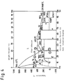
- Fig. 6 shows the result when position errors of the semiconductor laser diode in the lateral or horizontal direction are measured by marking the substrate and semiconductor laser. Because the junction structure is relatively thin, the influence of the surface tension of the melted AuSn eutectic layer can be suppressed. In addition, because the scrubbing process is not necessary, the position error is 0.46 ⁇ m in average, resulting in a good junction result.
- An initial junction strength is 80 gram in die shear strength and the degradation of it could not recognized even after application of heat cycle. More specifically, the stable junction structure was obtained by setting the weight % ratio of Au and Sn to be 80 : 20 in the junction portion of the optical circuit substrate and by shifting it from the eutectic state to a Au-richer state, compared to a case of the eutectic state maintained.
- the junction portion is provided on at least one of the optical semiconductor element and the optical circuit substrate and the junction portion includes the Au layer formed as the top layer and a layer in which Au layers and Sn layers are laminated and Au and Sn are made eutectic.
- the optical semiconductor element is joined with the optical circuit substrate by the eutectic.
- the optical semiconductor element can be positioned with a precision of submicron order.
- the state of the junction structure is shifted from the eutectic state of Au and Sn to the Au-richer state than the eutectic state, so that the junction structure stable even in a high temperature can be obtained.
Landscapes
- Die Bonding (AREA)
- Semiconductor Lasers (AREA)
- Led Device Packages (AREA)
Claims (4)
- Procédé de fabrication d'un dispositif optique à semi-conducteur, comprenant les étapes de :a) formation d'une première couche de Au (3) sur une partie de jonction (2) d'un substrat (1) ;b) formation d'une couche de Sn (4) sur ladite première couche de Au (3) ;c) formation d'une deuxième couche de Au (5) ayant une épaisseur d'environ 0,4 µm sur ladite couche de Sn (4) ;d) mise en contact de la surface de jonction (10) de l'élément optique à semi-conducteur (9) avec la partie de jonction (2) du substrat de circuit optique (1) ;e) pression dudit élément optique à semi-conducteur (9) sur ledit substrat de circuit optique ;f) chauffage du substrat de circuit optique (1) jusqu'à ce que la surface de jonction (10) soit mouillée avec le composé eutectique AuSn ; et,g) refroidissement du substrat de circuit optique (1) à la température ambiante, où le rapport des pourcentages en poids de Au et Sn est environ égal à 80 % : 20 %.
- Procédé selon la revendication 1, dans lequel le total des épaisseurs de la sous-couche de Au (3), de la couche de Sn (4) et de la sous-couche de Au (5) est dans la plage de 1 à 2 µm.
- Procédé selon la revendication 1 ou 2, dans lequel ladite étape de chauffage comprend un chauffage du substrat de circuit optique (1) à une température de 280°C ou plus.
- Procédé selon l'une quelconque des revendications 1 à 3, dans lequel une couche de barrière (8) est formée entre le substrat (2) et la première couche de Au (3), la couche de barrière (8) incluant une couche de titane (Ti) (6) et une couche de platine (Pt) (7) formée sur celle-ci.
Applications Claiming Priority (3)
| Application Number | Priority Date | Filing Date | Title |
|---|---|---|---|
| JP12511493 | 1993-04-27 | ||
| JP125114/93 | 1993-04-27 | ||
| JP12511493 | 1993-04-27 |
Publications (2)
| Publication Number | Publication Date |
|---|---|
| EP0622837A1 EP0622837A1 (fr) | 1994-11-02 |
| EP0622837B1 true EP0622837B1 (fr) | 2000-10-11 |
Family
ID=14902196
Family Applications (1)
| Application Number | Title | Priority Date | Filing Date |
|---|---|---|---|
| EP94106599A Expired - Lifetime EP0622837B1 (fr) | 1993-04-27 | 1994-04-27 | Méthode de fabrication d'un dispositif semi-conducteur |
Country Status (3)
| Country | Link |
|---|---|
| US (2) | US5917200A (fr) |
| EP (1) | EP0622837B1 (fr) |
| DE (1) | DE69426090T2 (fr) |
Families Citing this family (25)
| Publication number | Priority date | Publication date | Assignee | Title |
|---|---|---|---|---|
| US6027957A (en) * | 1996-06-27 | 2000-02-22 | University Of Maryland | Controlled solder interdiffusion for high power semiconductor laser diode die bonding |
| JPH10223690A (ja) * | 1997-02-13 | 1998-08-21 | Nec Corp | 光素子の実装方法 |
| DE19730118B4 (de) | 1997-07-14 | 2006-01-12 | Infineon Technologies Ag | Verfahren und Vorrichtung zur Herstellung einer Chip-Substrat-Verbindung |
| EP0926744B8 (fr) | 1997-12-15 | 2008-05-21 | Philips Lumileds Lighting Company, LLC. | Dispositif émetteur de lumière |
| US6265240B1 (en) * | 1998-03-24 | 2001-07-24 | Lucent Technologies, Inc. | Method and apparatus for passively aligning components on semiconductor dies |
| WO1999050901A1 (fr) * | 1998-03-30 | 1999-10-07 | Yamatake Corporation | Matiere de brasage tendre utilise pour fixer des puces |
| US6222207B1 (en) * | 1999-05-24 | 2001-04-24 | Lumileds Lighting, U.S. Llc | Diffusion barrier for increased mirror reflectivity in reflective solderable contacts on high power LED chip |
| US6214646B1 (en) * | 2000-02-29 | 2001-04-10 | Lucent Technologies Inc. | Soldering optical subassemblies |
| JP2002289768A (ja) * | 2000-07-17 | 2002-10-04 | Rohm Co Ltd | 半導体装置およびその製法 |
| US6946685B1 (en) | 2000-08-31 | 2005-09-20 | Lumileds Lighting U.S., Llc | Light emitting semiconductor method and device |
| JP3409781B2 (ja) * | 2000-09-05 | 2003-05-26 | 住友電気工業株式会社 | 光半導体モジュールの製造方法 |
| JP4131623B2 (ja) * | 2001-09-12 | 2008-08-13 | 三洋電機株式会社 | 電極構造およびその製造方法 |
| JP4136648B2 (ja) * | 2002-12-26 | 2008-08-20 | 日本碍子株式会社 | 異種材料接合体及びその製造方法 |
| JP4906256B2 (ja) * | 2004-11-10 | 2012-03-28 | 株式会社沖データ | 半導体複合装置の製造方法 |
| JP4950557B2 (ja) * | 2005-05-31 | 2012-06-13 | 三洋電機株式会社 | 半導体発光装置 |
| WO2007119571A1 (fr) * | 2006-04-17 | 2007-10-25 | Dowa Electronics Materials Co., Ltd. | couche de brasage, substrat pour jonction de dispositif utilisant ladite couche, et processus de fabrication du substrat |
| JP5526336B2 (ja) * | 2007-02-27 | 2014-06-18 | Dowaエレクトロニクス株式会社 | 半田層及びそれを用いたデバイス接合用基板並びにその製造方法 |
| JP4341693B2 (ja) * | 2007-05-16 | 2009-10-07 | ウシオ電機株式会社 | Led素子およびその製造方法 |
| KR101266205B1 (ko) * | 2008-07-08 | 2013-05-21 | 우시오덴키 가부시키가이샤 | 발광 장치 및 발광 장치의 제조 방법 |
| KR101266226B1 (ko) * | 2008-07-09 | 2013-05-21 | 우시오덴키 가부시키가이샤 | 발광 장치 및 발광 장치의 제조 방법 |
| AT513747B1 (de) | 2013-02-28 | 2014-07-15 | Mikroelektronik Ges Mit Beschränkter Haftung Ab | Bestückungsverfahren für Schaltungsträger und Schaltungsträger |
| CN106298719A (zh) * | 2016-09-13 | 2017-01-04 | 江苏纳沛斯半导体有限公司 | 金属凸块结构及其形成方法 |
| CN107591338A (zh) * | 2017-08-11 | 2018-01-16 | 苏州孚尔唯系统集成有限公司 | 一种基于tlp扩散连接的电子封装方法 |
| JP7168280B2 (ja) * | 2018-06-26 | 2022-11-09 | 住友電工デバイス・イノベーション株式会社 | 半導体装置、および、半導体チップの搭載方法 |
| EP4002428B1 (fr) * | 2020-11-19 | 2023-11-01 | Murata Manufacturing Co., Ltd. | Méthode de fabrication d'un interposeur |
Citations (2)
| Publication number | Priority date | Publication date | Assignee | Title |
|---|---|---|---|---|
| JPH01138777A (ja) * | 1987-11-25 | 1989-05-31 | Mitsubishi Electric Corp | 光半導体素子用サブマウント |
| EP0585084A1 (fr) * | 1992-08-28 | 1994-03-02 | AT&T Corp. | Procédé de connexion métallique permanente |
Family Cites Families (8)
| Publication number | Priority date | Publication date | Assignee | Title |
|---|---|---|---|---|
| US3986255A (en) * | 1974-11-29 | 1976-10-19 | Itek Corporation | Process for electrically interconnecting chips with substrates employing gold alloy bumps and magnetic materials therein |
| GB2137131B (en) * | 1983-03-15 | 1986-06-25 | Standard Telephones Cables Ltd | Bonding semiconductive bodies |
| US4772935A (en) * | 1984-12-19 | 1988-09-20 | Fairchild Semiconductor Corporation | Die bonding process |
| US4929516A (en) * | 1985-03-14 | 1990-05-29 | Olin Corporation | Semiconductor die attach system |
| JPS6438777A (en) * | 1987-08-04 | 1989-02-09 | Minolta Camera Kk | Scattered toner capturing device |
| US5280414A (en) * | 1990-06-11 | 1994-01-18 | International Business Machines Corp. | Au-Sn transient liquid bonding in high performance laminates |
| US5197654A (en) * | 1991-11-15 | 1993-03-30 | Avishay Katz | Bonding method using solder composed of multiple alternating gold and tin layers |
| US5298735A (en) * | 1992-10-07 | 1994-03-29 | Eastman Kodak Company | Laser diode and photodetector circuit assembly |
-
1994
- 1994-04-27 DE DE69426090T patent/DE69426090T2/de not_active Expired - Fee Related
- 1994-04-27 EP EP94106599A patent/EP0622837B1/fr not_active Expired - Lifetime
-
1995
- 1995-05-25 US US08/452,653 patent/US5917200A/en not_active Expired - Fee Related
-
1996
- 1996-04-29 US US08/638,873 patent/US5854087A/en not_active Expired - Fee Related
Patent Citations (2)
| Publication number | Priority date | Publication date | Assignee | Title |
|---|---|---|---|---|
| JPH01138777A (ja) * | 1987-11-25 | 1989-05-31 | Mitsubishi Electric Corp | 光半導体素子用サブマウント |
| EP0585084A1 (fr) * | 1992-08-28 | 1994-03-02 | AT&T Corp. | Procédé de connexion métallique permanente |
Also Published As
| Publication number | Publication date |
|---|---|
| EP0622837A1 (fr) | 1994-11-02 |
| US5854087A (en) | 1998-12-29 |
| US5917200A (en) | 1999-06-29 |
| DE69426090T2 (de) | 2001-03-01 |
| DE69426090D1 (de) | 2000-11-16 |
Similar Documents
| Publication | Publication Date | Title |
|---|---|---|
| EP0622837B1 (fr) | Méthode de fabrication d'un dispositif semi-conducteur | |
| EP0229850B1 (fr) | Bornes de connection entre des substrats et procede de production | |
| EP0253691B1 (fr) | Procédé de montage d'un dé en silicium | |
| US4930001A (en) | Alloy bonded indium bumps and methods of processing same | |
| US7009299B2 (en) | Kinetically controlled solder | |
| EP2157605B1 (fr) | Appareil électronique et procédé de fabrication associé | |
| US20020090756A1 (en) | Semiconductor device and method of manufacturing the same | |
| US4980239A (en) | Metallization layer structure formed on aluminum nitride ceramics and method of producing the metallization layer structure | |
| JP2797958B2 (ja) | 光半導体素子接合構造と接合方法 | |
| US7670879B2 (en) | Manufacturing method of semiconductor module including solid-liquid diffusion joining steps | |
| US6121062A (en) | Process of fabricating semiconductor unit employing bumps to bond two components | |
| US6963676B2 (en) | Optical module and method of assembling the optical module | |
| JP4136844B2 (ja) | 電子部品の実装方法 | |
| JP4552934B2 (ja) | 電子部品の実装方法 | |
| US5242099A (en) | Method of die bonding semiconductor chip | |
| JP2003197982A (ja) | 金スズ接合ペルチェ素子熱電変換モジュール | |
| US7795732B2 (en) | Ceramic wiring board and process for producing the same, and semiconductor device using the same | |
| EP0844656A1 (fr) | Structure de composant electronique | |
| JP3243834B2 (ja) | 半田材及び接合方法 | |
| JP4605850B2 (ja) | 光実装基板の製造方法 | |
| JPH11204884A (ja) | ハンダ形成方法 | |
| US20020056742A1 (en) | Methods and systems for attaching substrates to one another using solder structures having portions with different melting points | |
| JPS61181136A (ja) | ダイボンデイング方法 | |
| JP4593717B2 (ja) | 回路基板及びそれを用いた回路装置 | |
| JPH1197618A (ja) | シリコンウェハーの接合方法 |
Legal Events
| Date | Code | Title | Description |
|---|---|---|---|
| PUAI | Public reference made under article 153(3) epc to a published international application that has entered the european phase |
Free format text: ORIGINAL CODE: 0009012 |
|
| AK | Designated contracting states |
Kind code of ref document: A1 Designated state(s): DE FR GB |
|
| 17P | Request for examination filed |
Effective date: 19940909 |
|
| 17Q | First examination report despatched |
Effective date: 19951206 |
|
| GRAG | Despatch of communication of intention to grant |
Free format text: ORIGINAL CODE: EPIDOS AGRA |
|
| RTI1 | Title (correction) |
Free format text: A METHOD OF MANUFACTURING AN OPTICAL SEMICONDUCTOR DEVICE |
|
| GRAG | Despatch of communication of intention to grant |
Free format text: ORIGINAL CODE: EPIDOS AGRA |
|
| GRAG | Despatch of communication of intention to grant |
Free format text: ORIGINAL CODE: EPIDOS AGRA |
|
| GRAH | Despatch of communication of intention to grant a patent |
Free format text: ORIGINAL CODE: EPIDOS IGRA |
|
| GRAH | Despatch of communication of intention to grant a patent |
Free format text: ORIGINAL CODE: EPIDOS IGRA |
|
| GRAA | (expected) grant |
Free format text: ORIGINAL CODE: 0009210 |
|
| AK | Designated contracting states |
Kind code of ref document: B1 Designated state(s): DE FR GB |
|
| REF | Corresponds to: |
Ref document number: 69426090 Country of ref document: DE Date of ref document: 20001116 |
|
| ET | Fr: translation filed | ||
| PLBE | No opposition filed within time limit |
Free format text: ORIGINAL CODE: 0009261 |
|
| STAA | Information on the status of an ep patent application or granted ep patent |
Free format text: STATUS: NO OPPOSITION FILED WITHIN TIME LIMIT |
|
| 26N | No opposition filed | ||
| REG | Reference to a national code |
Ref country code: GB Ref legal event code: IF02 |
|
| PGFP | Annual fee paid to national office [announced via postgrant information from national office to epo] |
Ref country code: FR Payment date: 20030408 Year of fee payment: 10 |
|
| PGFP | Annual fee paid to national office [announced via postgrant information from national office to epo] |
Ref country code: GB Payment date: 20030423 Year of fee payment: 10 |
|
| PGFP | Annual fee paid to national office [announced via postgrant information from national office to epo] |
Ref country code: DE Payment date: 20030508 Year of fee payment: 10 |
|
| PG25 | Lapsed in a contracting state [announced via postgrant information from national office to epo] |
Ref country code: GB Free format text: LAPSE BECAUSE OF NON-PAYMENT OF DUE FEES Effective date: 20040427 |
|
| PG25 | Lapsed in a contracting state [announced via postgrant information from national office to epo] |
Ref country code: DE Free format text: LAPSE BECAUSE OF NON-PAYMENT OF DUE FEES Effective date: 20041103 |
|
| GBPC | Gb: european patent ceased through non-payment of renewal fee |
Effective date: 20040427 |
|
| PG25 | Lapsed in a contracting state [announced via postgrant information from national office to epo] |
Ref country code: FR Free format text: LAPSE BECAUSE OF NON-PAYMENT OF DUE FEES Effective date: 20041231 |
|
| REG | Reference to a national code |
Ref country code: FR Ref legal event code: ST |