EP0624879A1 - Eintakt-Speicher mit Seitenmodus. - Google Patents
Eintakt-Speicher mit Seitenmodus. Download PDFInfo
- Publication number
- EP0624879A1 EP0624879A1 EP94301274A EP94301274A EP0624879A1 EP 0624879 A1 EP0624879 A1 EP 0624879A1 EP 94301274 A EP94301274 A EP 94301274A EP 94301274 A EP94301274 A EP 94301274A EP 0624879 A1 EP0624879 A1 EP 0624879A1
- Authority
- EP
- European Patent Office
- Prior art keywords
- mode
- page
- memory
- signal
- page mode
- Prior art date
- Legal status (The legal status is an assumption and is not a legal conclusion. Google has not performed a legal analysis and makes no representation as to the accuracy of the status listed.)
- Withdrawn
Links
- 230000015654 memory Effects 0.000 title claims abstract description 79
- 238000000034 method Methods 0.000 claims description 17
- 230000008569 process Effects 0.000 claims description 11
- 230000004044 response Effects 0.000 claims description 6
- 238000001514 detection method Methods 0.000 claims 5
- 238000010586 diagram Methods 0.000 description 7
- 230000007704 transition Effects 0.000 description 7
- 230000004913 activation Effects 0.000 description 4
- 230000006870 function Effects 0.000 description 4
- 230000007274 generation of a signal involved in cell-cell signaling Effects 0.000 description 2
- 230000000977 initiatory effect Effects 0.000 description 2
- 230000004048 modification Effects 0.000 description 2
- 238000012986 modification Methods 0.000 description 2
- 230000000295 complement effect Effects 0.000 description 1
- 230000003111 delayed effect Effects 0.000 description 1
Images



Classifications
-
- G—PHYSICS
- G11—INFORMATION STORAGE
- G11C—STATIC STORES
- G11C7/00—Arrangements for writing information into, or reading information out from, a digital store
- G11C7/10—Input/output [I/O] data interface arrangements, e.g. I/O data control circuits, I/O data buffers
- G11C7/1015—Read-write modes for single port memories, i.e. having either a random port or a serial port
- G11C7/1018—Serial bit line access mode, e.g. using bit line address shift registers, bit line address counters, bit line burst counters
- G11C7/1021—Page serial bit line access mode, i.e. using an enabled row address stroke pulse with its associated word line address and a sequence of enabled column address stroke pulses each with its associated bit line address
Definitions
- the present invention relates to a single clock memory that can execute a page mode.
- the single clock memory is a memory which takes in both row and column addresses in response to a single clock signal.
- Figure 8 shows a typical circuit configuration of this type of dynamic random access memory (DRAM).
- DRAM dynamic random access memory
- the double clock memory is a memory which takes in both row and column addresses at different times using address multiplexing.
- Figure 9 shows a typical circuit configuration of a double clock memory DRAM.
- row and column addresses are applied sequentially to the same address input terminals A0 through A10, the row address being loaded into a row address buffer by row address strobe signal -RAS (negative polarity signal of RAS), the column address being loaded into a column address buffer by a column address strobe signal -CAS (negative polarity signal of CAS).
- the double clock DRAM latches (holds) the row address and the sense amplifier of the memory cell array latches data, which allows data access called page mode to be implemented in the double clock DRAM.
- the page mode is a mode of accessing individual memory cells by fixing one row address provided to the DRAM, and then continuously providing different column addresses to the DRAM.
- the single clock DRAM makes it a condition that row and column addresses are generated simultaneously and the row circuits (such as the sense amplifier) and the column circuits are controlled by a single external clock. Consequently, terminating an access to a memory cell resets the row and column addresses latched in the memory. As a result, there exists a problem that the single clock DRAM cannot implement the page mode that is allowed with the double clock DRAM.
- the page mode cannot be immediately performed.
- the page mode and the ordinary mode differ from each other in the control process within the memory.
- the page mode requires modification of the control process performed in the ordinary mode. That is, the page mode requires execution of the memory control process specific to each phase or state of the page mode, such as "start of page mode,” “during-page mode” and "end of page mode.” So it requires identifying these operation states.
- the simplest method for identifying the operation mode states is to use two bits to identify the above states but this method requires the addition of two external control lines, and is not preferable.
- an object of the present invention is to allow the page mode to be executed with ease in a single clock memory which takes in both row and column addresses in response to a single external clock signal.
- Another object of the invention is to provide a simple method for setting the page mode in the single clock memory and identifying the state thereof.
- a slight modification of the memory control circuit allows a page mode function to be incorporated into an ordinary single clock memory.
- the page mode requires control processes specific to the page mode, such as the row address holding function. This can be easily done by modifying the memory circuit so that the control steps ordinarily performed in the single clock memory are partly omitted.
- the single clock memory of the present invention has a state identification circuit for identifying the operation mode state such as the start of page mode, during-page mode, and end of page mode.
- the mode state identification circuit receives a single control signal, the first level of which indicates the ordinary mode, and the second level of which indicates the page mode, to determine the mode state based on the combination of the levels of the control signal in consecutive memory cycles.
- the single clock memory of the present invention further comprises a memory control means for performing predetermined memory control processes in correspondence with the state identified by the mode state identifying circuit.
- the memory control means selectively omits part of the memory control operations performed in the ordinary mode to result in the operation of the page mode.
- the present invention provides a method for setting the page mode in a single clock memory and determining the state of the page mode.
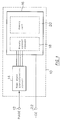
- Figure 1 shows a schematic circuit configuration in which the present invention is applied.
- the single clock memory 10 of the present invention has a newly added control input terminal 12 and a mode state identification circuit 14.
- a 1 bit external control signal PAGE is applied to the control input terminal 12 from a controller such as a processor.
- the control signal PAGE is inputted when row/column address signals are inputted.
- the control signal PAGE selectively designates the ordinary mode and the page mode and is further used to identify the mode states of "start of page mode" (hereinafter referred to as page-in), "during-page mode” (hereinafter referred to as during-page) and "end of page mode” (hereinafter referred to as page-out).
- the mode state identification circuit 14 decodes the control signal to identify the mode state.
- Signals representing the four mode states are transmitted to a memory array 16.
- the memory array 16 includes a memory cell part 20 for storing data and a memory control circuit part 18 for controlling the memory operation.
- the output of the mode state identification circuit 14 is applied to the memory control circuit part 18 so that the memory array 16 is controlled and processed depending on the identified state.
- a chip-enable signal -CE supplied to a terminal 22 corresponds to the single clock signal inputted to the single clock memory from the outside.
- the external control signal PAGE indicates the ordinary mode by a first level and the page mode by a second level.
- the mode state identification circuit 14 detects the levels of the control signal in two consecutive memory cycles (preceding and current cycles) to identify the afore-mentioned four mode states by decoding the detected levels.
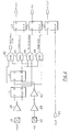
- the PAGE signal applied to the terminal 12 from the outside indicates the page mode by a high level and the ordinary mode by a low level.
- the PAGE signal is applied to the data input D in a latch L1 via an inverter 26 while the output Q of the latch L1 is supplied to the data input D of a latch L2.
- the external clock signal -CE to the terminal 22 is applied to the clock input CLK of the latch L1 via an inverter 28.
- the output of the inverter 28 is applied to the clock input of the latch L2 via an inverter 30.
- the outputs Q of the latch L1 and the latch L2 are applied to a logic AND gate 32.
- the inverted output of the latch L1 and the output Q of the latch 2 are applied to an AND gate 34.
- the inverted outputs of the latches L1 and L2 are applied to an AND gate 36.
- the output Q of the latch L1 and the inverted output of the latch L2 are applied to an AND gate 38.
- the PAGE signal is loaded into the latch L1 by the negative transition of the clock signal -CE generated at the time of the initiation of each memory cycle.
- the output Q of the latch L1 is taken in the latch L2 by the positive transition of the clock signal -CE delayed by the inverter 30.
- the PAGE signal is loaded into the latch L1 by the negative transition of the next clock signal -CE and the output of the latch L1 is transferred to the latch L2 by the next positive transition.
- the latch L1 detects the level of the PAGE signal in the current memory cycle whereas the latch L2 detects the level of the PAGE signal in the immediately preceding memory cycle.
- the AND gates 32, 34, 36, and 38 decode the combinations of the levels in these two cycles to identify the operation mode states.
- the combinations of the levels of the PAGE signal represents the following operation mode states. "H” designates a high level and "L” designates a low level.
- the output signals of the AND gates 32, 34, 36, and 38 represent the ordinary mode, the page-in, during-page, and the page-out.
- the page-in, during-page, and page-out signals are gotten into the latches L3, L4, and L5 by the clock signal CLK which is generated internally in response to -CE and supplied to terminal 40.
- the outputs of these latches provide page-in signal PGIN, during-page signal PG, and page-out signal PGOUT which are applied to the memory control circuit part 18 ( Figure 1) for page mode control.
- the output of the ordinary mode is not employed in this embodiment, but may be employed for a particular purpose depending on the control technique to be used.
- the page mode requires a control process differing from the ordinary mode in each of the page-in, during-page, and page-out mode states.
- each of the states of the ordinary mode, page-in, during-page, and page-out will be briefly described.
- the ordinary mode is a memory access mode in which row and column addresses are simultaneously taken in by the external clock signal -CE. In the ordinary mode, row and column addresses are reset after memory access.
- the page-in is a mode state indicating that a row address is to be held in the memory. This mode state requires the resetting of column address only.
- the during-page is a mode state indicating that the memory access is performed in response to the row address held in the memory and column address inputted in each memory cycle.
- This mode state requires the reset of only column address after each memory access.
- the page-out is a mode state indicating that the held row address and the column address in the last memory cycle of the page mode are to be reset after the memory access.
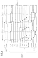
- FIG. 6 and Figure 7 are a timing chart showing the ordinary mode of a representative DRAM and the page mode incorporated in accordance with the present invention.
- -CE is a single external clock signal, which generates a negative transition at the time of the initiation of each memory cycle.
- the PAGE signal has a settled level at the time of the negative transition of the clock signal -CE.
- CLK is an internal clock signal
- RATCG is a row address T/C (true/complement) drive signal used for the holding and decoding of row addresses
- WLD is a word line drive signal
- WL is a word line voltage waveform
- SET is a sense amplifier activation signal
- BLPCEQ is a bit line precharge/equalize signal
- CATCG is a column address T/C drive signal used for the holding and decoding of column addresses
- DLPCEQ is a data line precharge/equalize signal
- BSDRV is a bit switch drive signal.
- the control processing necessary for the page mode can be easily implemented by selectively omitting part of the control processes in the ordinary mode.
- the control processes to be omitted in the page mode are as follows. Cycle Processes to be omitted page-in - resetting of word line - resetting of sense amplifier - precharging an equalization of bit line during-page - loading and decoding of row address - driving of word line - activation of sense amplifier - resetting of word line - resetting of sense amplifier - precharging and equalization of bit line page-out - loading and decoding of row address - driving of word line - activation of sense amplifier
- the resetting of the word line drive signal is omitted to hold the selected word line in driven state. This causes the resetting of RATCG to be omitted, thus holding the row address.
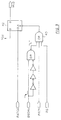
- the omission of the resetting of the word line drive (WLD) is performed with a circuit shown in Figure 3.
- the PGIN signal and PG signal are at a low level.
- the OR 40 gate Upon the negative transition of the BSDRV the OR 40 gate generates a low level to reset the latch 42.
- the PGIN signal or the PG signal go to a high level to remove the reset signal from the latch 42.
- the omission of the word line resetting in turn results in the omission of the resetting of the sense amplifier (SET) and the setting of the bit line precharge/equalize (BLPCEQ).
- RATCG row address
- WLD/WL driving of word line
- SET activation of sense amplifier
- the timing of the column circuits needs to be modified.
- the column signals relating to data transfer to or from the outside (DLPCEQ and BSDRV in this example) must be operated after the completion of the row operation. Consequently, as shown in Figure 6 and Figure 7, in the ordinary mode and page-in, WLD resets the DLPCEQ and SET sets BSDRV.
- the row access phase is already terminated during the page-in and the operation of the row circuits is completed. Thus, the operation of the column circuits cannot be controlled in response to the operation of the row circuits.
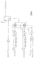
- the column circuit timing is modified so that CATCG resets DLPCEQ and then sets BSDRV. This is carried out with the circuits shown in Figure 4 and Figure 5.
- Symbol G designates a transfer gate in which PMOS FET and NOMS FET are connected in parallel.
- DLPCEQ is set by BSDRV and reset by WLD.
- DLPCEQ is reset when either the PG signal or PGOUT signal is high and the CATCG signal goes high as well.
- the BSDRV signal is set by SET in the ordinary mode and in the page-in cycle.
- the BSDRV signal is set when either the PG signal or the PGOUT signal is high and the DLPCEQ signal goes low.
- the present invention is applicable to the case where the page mode is incorporated into a single clock SRAM.
- the PAGE signal may denote the ordinary mode by a high level and the page mode by a low level.
- other circuits can be used to control the memory based on the identification by the identification circuit 14.
- the present invention can realize the memory access in page mode in a single clock memory. Only one signal line needs to be used for designating the page mode, which does not inhibit the miniaturization of the memory.
Landscapes
- Dram (AREA)
Applications Claiming Priority (2)
| Application Number | Priority Date | Filing Date | Title |
|---|---|---|---|
| JP63888/93 | 1993-03-23 | ||
| JP06388893A JP3344494B2 (ja) | 1993-03-23 | 1993-03-23 | ページモードを有するシングルクロックメモリ |
Publications (1)
| Publication Number | Publication Date |
|---|---|
| EP0624879A1 true EP0624879A1 (de) | 1994-11-17 |
Family
ID=13242287
Family Applications (1)
| Application Number | Title | Priority Date | Filing Date |
|---|---|---|---|
| EP94301274A Withdrawn EP0624879A1 (de) | 1993-03-23 | 1994-02-23 | Eintakt-Speicher mit Seitenmodus. |
Country Status (3)
| Country | Link |
|---|---|
| US (1) | US5410514A (de) |
| EP (1) | EP0624879A1 (de) |
| JP (1) | JP3344494B2 (de) |
Cited By (3)
| Publication number | Priority date | Publication date | Assignee | Title |
|---|---|---|---|---|
| WO1996020480A1 (en) * | 1994-12-23 | 1996-07-04 | Micron Technology, Inc. | System adapted to receive multiple memory types |
| FR2812752A1 (fr) * | 2000-08-05 | 2002-02-08 | Samsung Electronics Co Ltd | Dispositif a memoire, systeme de memoire et procede pour acceder a des donnees en memoire |
| EP1398785A3 (de) * | 2002-08-29 | 2005-02-09 | Fujitsu Limited | Halbleiterspeicher |
Families Citing this family (3)
| Publication number | Priority date | Publication date | Assignee | Title |
|---|---|---|---|---|
| US6035369A (en) | 1995-10-19 | 2000-03-07 | Rambus Inc. | Method and apparatus for providing a memory with write enable information |
| US6209071B1 (en) | 1996-05-07 | 2001-03-27 | Rambus Inc. | Asynchronous request/synchronous data dynamic random access memory |
| US5940345A (en) * | 1997-12-12 | 1999-08-17 | Cypress Semiconductor Corp. | Combinational logic feedback circuit to ensure correct power-on-reset of a four-bit synchronous shift register |
Citations (2)
| Publication number | Priority date | Publication date | Assignee | Title |
|---|---|---|---|---|
| EP0420268A2 (de) * | 1989-09-29 | 1991-04-03 | Kabushiki Kaisha Toshiba | Betriebsartenwählerschaltung |
| EP0447624A2 (de) * | 1989-12-28 | 1991-09-25 | International Business Machines Corporation | Mehrfache Speichermodusauswahl für IC-Speicherchip |
Family Cites Families (13)
| Publication number | Priority date | Publication date | Assignee | Title |
|---|---|---|---|---|
| JPS58166579A (ja) * | 1982-03-29 | 1983-10-01 | Fujitsu Ltd | メモリ制御方式 |
| JPS5960594A (ja) * | 1982-09-29 | 1984-04-06 | 富士通株式会社 | 紙幣取扱装置 |
| US4876671A (en) * | 1985-04-30 | 1989-10-24 | Texas Instruments Incorporated | Semiconductor dynamic memory device with metal-level selection of page mode or nibble mode |
| US4685084A (en) * | 1985-06-07 | 1987-08-04 | Intel Corporation | Apparatus for selecting alternate addressing mode and read-only memory |
| US4750839A (en) * | 1985-08-07 | 1988-06-14 | Texas Instruments Incorporated | Semiconductor memory with static column decode and page mode addressing capability |
| JPS62139198A (ja) * | 1985-12-11 | 1987-06-22 | Mitsubishi Electric Corp | 半導体記憶装置 |
| JPS634492A (ja) * | 1986-06-23 | 1988-01-09 | Mitsubishi Electric Corp | 半導体記憶装置 |
| JPS63248000A (ja) * | 1987-04-02 | 1988-10-14 | Matsushita Electronics Corp | 不揮発性半導体メモリ |
| JPH01146193A (ja) * | 1988-09-21 | 1989-06-08 | Hitachi Ltd | 半導体記憶装置 |
| JPH0287399A (ja) * | 1988-09-22 | 1990-03-28 | Nec Ic Microcomput Syst Ltd | 半導体メモリのテスト方式 |
| JPH03113794A (ja) * | 1989-09-22 | 1991-05-15 | Toshiba Corp | 半導体記憶装置 |
| US4970418A (en) * | 1989-09-26 | 1990-11-13 | Apple Computer, Inc. | Programmable memory state machine for providing variable clocking to a multimode memory |
| JPH03238694A (ja) * | 1990-02-15 | 1991-10-24 | Matsushita Electric Ind Co Ltd | 半導体メモリ |
-
1993
- 1993-03-23 JP JP06388893A patent/JP3344494B2/ja not_active Expired - Fee Related
-
1994
- 1994-02-23 EP EP94301274A patent/EP0624879A1/de not_active Withdrawn
- 1994-03-21 US US08/215,245 patent/US5410514A/en not_active Expired - Fee Related
Patent Citations (2)
| Publication number | Priority date | Publication date | Assignee | Title |
|---|---|---|---|---|
| EP0420268A2 (de) * | 1989-09-29 | 1991-04-03 | Kabushiki Kaisha Toshiba | Betriebsartenwählerschaltung |
| EP0447624A2 (de) * | 1989-12-28 | 1991-09-25 | International Business Machines Corporation | Mehrfache Speichermodusauswahl für IC-Speicherchip |
Non-Patent Citations (1)
| Title |
|---|
| INTEL: "INTEL COMPONENT DATA CATALOG 1978", 1978, INTEL, SANTA CLARA,USA * |
Cited By (4)
| Publication number | Priority date | Publication date | Assignee | Title |
|---|---|---|---|---|
| WO1996020480A1 (en) * | 1994-12-23 | 1996-07-04 | Micron Technology, Inc. | System adapted to receive multiple memory types |
| FR2812752A1 (fr) * | 2000-08-05 | 2002-02-08 | Samsung Electronics Co Ltd | Dispositif a memoire, systeme de memoire et procede pour acceder a des donnees en memoire |
| EP1398785A3 (de) * | 2002-08-29 | 2005-02-09 | Fujitsu Limited | Halbleiterspeicher |
| US6963518B2 (en) | 2002-08-29 | 2005-11-08 | Fujitsu Limited | Semiconductor memory having a pulse generator for generating column pulses |
Also Published As
| Publication number | Publication date |
|---|---|
| JP3344494B2 (ja) | 2002-11-11 |
| JPH06275066A (ja) | 1994-09-30 |
| US5410514A (en) | 1995-04-25 |
Similar Documents
| Publication | Publication Date | Title |
|---|---|---|
| US5155705A (en) | Semiconductor memory device having flash write function | |
| US4344156A (en) | High speed data transfer for a semiconductor memory | |
| EP0135940B1 (de) | Doppeltor-Speicheranordnung | |
| KR100386442B1 (ko) | 메모리디바이스회로 및 멀티뱅크메모리어레이의 멀티뱅크컬럼의동시어드레스방법 | |
| KR100401506B1 (ko) | 비동기 프리차지 기능을 갖는 싱크로노스 메모리 디바이스 | |
| US6208582B1 (en) | Memory device including a double-rate input/output circuit | |
| US5379263A (en) | Semiconductor memory device which can provide required data flexibly under simplified control and operating method therefor | |
| EP0452510B1 (de) | Halbleiterspeicheranordnung | |
| US6192003B1 (en) | Semiconductor memory device using a relatively low-speed clock frequency and capable of latching a row address and a column address with one clock signal and performing a page operation | |
| KR950007450B1 (ko) | 고속으로 데이타의 소거가 가능한 ram | |
| US6175894B1 (en) | Memory device command buffer apparatus and method and memory devices and computer systems using same | |
| EP0311047B1 (de) | Dynamischer RAM-Speicher | |
| US5973993A (en) | Semiconductor memory burst length count determination detector | |
| US5608688A (en) | DRAM having output control circuit | |
| US4802134A (en) | Semiconductor memory device having serial addressing scheme | |
| US4602356A (en) | Semiconductor memory device | |
| US5936897A (en) | Semiconductor storage device capable of fast writing operation | |
| US5410514A (en) | Single clock memory having a page mode | |
| US5943288A (en) | Apparatus and method for minimizing address hold time in asynchronous SRAM | |
| US5561639A (en) | Semiconductor memory device with high speed detect function | |
| US4758991A (en) | Rewritable semiconductor memory device having a decoding inhibit function | |
| KR100253354B1 (ko) | 반도체 메모리의 동작 검사장치 | |
| JPH0628893A (ja) | 半導体記憶装置 | |
| US20010017787A1 (en) | Semiconductor memory device | |
| US5629896A (en) | Write controlled address buffer |
Legal Events
| Date | Code | Title | Description |
|---|---|---|---|
| PUAI | Public reference made under article 153(3) epc to a published international application that has entered the european phase |
Free format text: ORIGINAL CODE: 0009012 |
|
| AK | Designated contracting states |
Kind code of ref document: A1 Designated state(s): DE FR GB |
|
| 17P | Request for examination filed |
Effective date: 19950117 |
|
| 17Q | First examination report despatched |
Effective date: 19970728 |
|
| GRAG | Despatch of communication of intention to grant |
Free format text: ORIGINAL CODE: EPIDOS AGRA |
|
| STAA | Information on the status of an ep patent application or granted ep patent |
Free format text: STATUS: THE APPLICATION IS DEEMED TO BE WITHDRAWN |
|
| 18D | Application deemed to be withdrawn |
Effective date: 19980901 |