EP0452510B1 - Halbleiterspeicheranordnung - Google Patents
Halbleiterspeicheranordnung Download PDFInfo
- Publication number
- EP0452510B1 EP0452510B1 EP90916367A EP90916367A EP0452510B1 EP 0452510 B1 EP0452510 B1 EP 0452510B1 EP 90916367 A EP90916367 A EP 90916367A EP 90916367 A EP90916367 A EP 90916367A EP 0452510 B1 EP0452510 B1 EP 0452510B1
- Authority
- EP
- European Patent Office
- Prior art keywords
- signal
- row address
- timing
- row
- address
- Prior art date
- Legal status (The legal status is an assumption and is not a legal conclusion. Google has not performed a legal analysis and makes no representation as to the accuracy of the status listed.)
- Expired - Lifetime
Links
Images




Classifications
-
- G—PHYSICS
- G11—INFORMATION STORAGE
- G11C—STATIC STORES
- G11C11/00—Digital stores characterised by the use of particular electric or magnetic storage elements; Storage elements therefor
- G11C11/21—Digital stores characterised by the use of particular electric or magnetic storage elements; Storage elements therefor using electric elements
- G11C11/34—Digital stores characterised by the use of particular electric or magnetic storage elements; Storage elements therefor using electric elements using semiconductor devices
- G11C11/40—Digital stores characterised by the use of particular electric or magnetic storage elements; Storage elements therefor using electric elements using semiconductor devices using transistors
- G11C11/401—Digital stores characterised by the use of particular electric or magnetic storage elements; Storage elements therefor using electric elements using semiconductor devices using transistors forming cells needing refreshing or charge regeneration, i.e. dynamic cells
- G11C11/4063—Auxiliary circuits, e.g. for addressing, decoding, driving, writing, sensing or timing
- G11C11/407—Auxiliary circuits, e.g. for addressing, decoding, driving, writing, sensing or timing for memory cells of the field-effect type
- G11C11/4076—Timing circuits
-
- G—PHYSICS
- G11—INFORMATION STORAGE
- G11C—STATIC STORES
- G11C8/00—Arrangements for selecting an address in a digital store
- G11C8/18—Address timing or clocking circuits; Address control signal generation or management, e.g. for row address strobe [RAS] or column address strobe [CAS] signals
Definitions
- the present invention relates to a semiconductor storage device, and particularly to an address multiplexed semiconductor storage device.
- DRAM dynamic random access memory
- the contents of all the memory cells in a specified row are read by a sense amplifier, and the contents are rewritten in the same memory cells, thus completing the basic operating cycle. If the contents pf all of the bits in a specified column are read and output externally, the operation is a read cycle. If the contents of the bits in a specified column are changed before rewriting, the operation is a write cycle. If both processes are executed, the operation is a read (modify) write cycle.
- a row is read, and a column is selected thereafter, wherein a row address and a column address are supplied using a time division or a so-called multiplex method.
- the multiplexed row address signal and column address signal are obtained in accordance with a row address strobe signal (hereinafter, RAS ⁇ ) and a column address strobe signal (hereinafter CAS ⁇ ). Both of these strobe signals are negative logic signals and the falling edge is defined as an address signal fetch timing.
- RAS ⁇ row address strobe signal
- CAS ⁇ column address strobe signal
- the signal is changed from inactive to active at the falling edge, and is changed from active to inactive at the rising edge.
- a circuit is precharged at the rising edge of the RAS ⁇ , at the falling of the RAS ⁇ a circuit on the row side is operated dynamically and the row address signal is fetched. Then, after the content of the signal is decoded and one of word lines is selected and activated, a circuit on the column side is operated dynamically at the falling of the CAS ⁇ and the column address signal is fetched. Further, the content of the signal is decoded, one bit line is selected, and one memory cell connected to the above one word line and one bit line is accessed.
- a DRAM using a socalled fast column method wherein each circuit is precharged at the rising of the RAS ⁇ , at an appropriate time after the falling of the RAS ⁇ an internal timing signal is generated, and in accordance with this signal, the column address is automatically fetched.
- a memory cell can be accessed without waiting for the falling of the CAS ⁇ , and a high speed operation can be planned.
- An object of the present invention is to provide a semiconductor storage device wherein the access start time is advanced more than the falling time of the RAS ⁇ , in the address fetching time for the memory, and a higher access speed is made possible.
- a semiconductor storage device comprising a first timing circuit for generating a first timing signal in response to an inactivation of a row address strobe signal; a row decoder for decoding a row address; and a word driver, connected to the row decoder, selecting a word line and being activated in response to a second timing signal; characterized in that it further comprises : a second timing circuit for generating said second timing signal in response to an activation of the row address strobe signal after the inactivation of said row address strobe signal; an address change detection circuit for generating an address change detection signal in response to a change of the row address occurring during period between the inactivation and activation of the row address strobe signal; and in that said row decoder decodes a row address for subsequent access in response to the first timing signal and decodes a changed row address signal in response to the second timing signal when the address change detection signal is generated.
- the present invention also relates to a data access method of a semiconductor storage device as indicated in claim 4.
- the row address signal is fetched and decoded at a rising time of the row address strobe signal ( RAS ⁇ ), and the word line is activated at a falling time of the RAS ⁇ . If at the falling time of the RAS ⁇ , the content of the row address signal has been changed, however, the content after that change is decoded and the word line is activated.
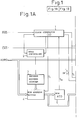
- Figure 1 is a block diagram showing an embodiment of a semiconductor storage device according to the present invention, as an example applied to a DRAM.
- Fig. 1 denotes a clock generator (A)
- 2 denotes a mode controller
- 3 denotes a refresh address counter
- 4 denotes a row address buffer
- 5 denotes a row address transition detector (hereinafter, row ATD)
- 6 denotes an AND gate
- 7 denotes a clock generator (B)
- 8 denotes a column address buffer
- 9 denotes a column address transition detector (hereinafter, column ATD)
- 10 denotes a write clock generator
- 11 denotes a data input buffer
- 12 denotes a data output buffer
- 13 denotes a row decoder
- 14 denotes a word driver
- 15 denotes a column decoder
- 16 denotes a sense amplifier I/O gate
- 17 denotes a memory cell array.
- RAS ⁇ is a row address strobe signal
- CAS ⁇ is a column address strobe signal
- ADRS is a row/column address signal
- WE ⁇ is a write enable signal
- DIN is input data
- DOUT is output data
- T1 to T4 are timing signals
- S A is an address change signal.
- the clock generator (A) 1 functions as a first timing circuit and a second timing circuit. Namely, it detects a rising edge and a falling edge of the RAS ⁇ and when detecting these signals, outputs the following timing signals.
- the T3 in the above signals is output also at the timing (2) (T3 with an asterisk *) only when the S A is output from the row ATD 5.
- the row ATD 5 functions as an address change detection circuit, the content of the row address signal which is input through the row address buffer 4 is monitored, and the content of the row address signal at the rising time of the RAS ⁇ is compared with that at the falling time. Then, if the content changes, the signal S A is output.
- the row decoder 13 decodes the content of the row address signal and selects one of word lines in accordance with the T3 ( ⁇ T3). Namely, the row decoder 13:
- the word driver 14 receives the above decoded output and starts to activate the selected word line in accordance with the falling time (T4) of the RAS ⁇ .
- the clock generator (B) 7 obtains information of the rising time (T4) of the RAS ⁇ and the falling time of the CAS ⁇ through the AND gate 6, and simultaneously executes the fast column function by controlling the column address buffer 8 or the column ATD 9, and by automatically fetching the column address signal after the predetermined time from the falling time of the RAS ⁇ .
- the row address buffer 4, the row ATD 5, and the row decoder 13 on the row address input side are circuits which operate statically.
- these elements are constituted by CMOS, low power consumption can be easily accomplished using a small number of elements. It is also possible to constitute a static operation circuit using n or p MOS transistors.
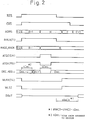
- the row address signal is fetched from the row address buffer 4 to the row ATD 5 and the row decoder 13, and the row decoder 13 decodes the content (ROW) thereof.
- the RAS ⁇ falls and the T4 is output
- the decoded signal is received, and the word driver 14 activates one word line.
- the column address signal is fetched automatically in accordance with a flow-through latch function, the content (Column) thereof is decoded, and one bit line is selected. As a result, for example, if the operation is a read cycle, the output data is read at the DOUT.
- the start time of the activation of the word line can be advanced in time as much as necessary for the word line selection.
- the row address access time (tRAC) from the falling time of the RAS ⁇ until the acquisition of the output data (in the case of a read cycle) can be decreased.
- the row address signal is input, so a high speed access can be carried out.
- the address input definition is not satisfied or when the user wishes to use the DRAM as a usual DRAM.
- the row address signal is usually defined at the falling time of the RAS ⁇ , the content of the row address signal is not clear before the falling of the RAS ⁇ .
- the wrong result is generated, the change of the content of the row address signal between the rising time and the falling time of the RAS ⁇ is detected, and until the detected result is obtained, the word line is not activated, in this embodiment.
- the usual fetching of the row address signal is executed and the compatibility with the conventional DRAM can be also secured.
- the row address access time (tRAC) is decreased and a higher access speed can be realized.
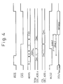
- Figure 3 and Fig. 4 are timing charts for explaining a conventional example.
- Fig. 3 shows the timing of a usual DRAM
- Fig. 4 shows the timing when only the fast column method is executed. Namely, in Fig. 3, the address decodes the row and the column start at the falling of the RAS ⁇ and the CAS ⁇ , respectively, however, in Fig. 4, the row address decoding starts at the falling of the RAS ⁇ , and after that the address decoding of the column address automatically starts. Comparing the timing chart of Fig. 3 with that of Fig. 4, the example in Fig. 4 operates at higher speed due to the advance of the start of decoding of the column address.
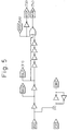
- the clock generator (A) (Fig. 5) outputs CBRZ for receiving the RAS ⁇ and for determining whether a normal mode or refresh mode is in effect, in response to the state of the CAS ⁇ , RASZ for controlling the input of the row address buffer, RALX (T1) for latching the address, ATDX (T3) for receiving ATDZ (SA) signal which is the signal from the ATD circuit for controlling the row decoder, and WLRX (T4) for controlling the word driver.
- CBRZ for receiving the RAS ⁇ and for determining whether a normal mode or refresh mode is in effect, in response to the state of the CAS ⁇
- RASZ for controlling the input of the row address buffer
- RALX (T1) for latching the address
- ATDX (T3) for receiving ATDZ (SA) signal which is the signal from the ATD circuit for controlling the row decoder
- WLRX (T4) for controlling the word driver.
- the row address buffer (Fig. 6) receives an external input signal ADRS and outputs complementary signals RADZ and RADX of the address.
- the refresh counter address (Q, Q ⁇ ) of the chip content is input, and the address signals RADZ and RADX are output.
- the row decoder and word driver receive the combined address input RAD ⁇ i ( ⁇ is Z or X, i is an address number) in response to the address, output a decode signal in accordance with the control signal ATDX (T3) from the clock generator (A), receive the word driver control signal WLRX (T4), and drive the word line WLSZ.
- the row ATD receives RADZi and RADXi (i is address number) from the respective complementary address signals RADZ and RADX, and outputs the ATDZ (SA).
- These logic elements are constituted to operate in a static manner.
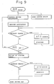
- Figure 9 is a flowchart for explaining the process steps of the semiconductor storage device according to this embodiment.
Landscapes
- Engineering & Computer Science (AREA)
- Microelectronics & Electronic Packaging (AREA)
- Computer Hardware Design (AREA)
- Dram (AREA)
- Static Random-Access Memory (AREA)
Claims (4)
- Halbleiterspeichervorrichtung, umfassend:eine erste Zeitgebungsschaltung (1) zum Erzeugen eines ersten Zeitgebungssignals (T1, T3) ansprechend auf eine Inaktivierung eines Reihenadressübernahmesignals
 einen Reihendecoder (13) zum Decodieren einer Reihenadresse (ADRS); undeinen Worttreiber (14), der mit dem Reihendecoder verbunden ist und eine Wortleitung auswählt und ansprechend auf ein zweites Zeitgebungssignal aktiviert wird;dadurch gekennzeichnet, daß sie ferner umfaßt:eine zweite Zeitgebungsschaltung (1) zum Erzeugen des zweiten Zeitgebungssignals (T1, ∗T3, T4) ansprechend auf eine Aktivierung des Reihenadressübernahmesignals nach der Inaktivierung des Reihenadressübernahmesignals;eine Adressänderungserfassungsschaltung (5) zum Erzeugen eines Adressänderungserfassungssignals (SA) ansprechend auf eine Änderung der Reihenadresse (ADRS), die während des Zeitraumes zwischen der Inaktivierung und der Aktivierung des Reihenadressübernahmesignals auftritt; und dadurch, daß der Reihendecoder (13) eine Reihenadresse für den nachfolgenden Zugriff ansprechend auf das erste Zeitgebungssignal (T1, T3) decodiert und ein geändertes Reihenadressignal ansprechend auf das zweite Zeitgebungssignal decodiert, wenn das Adressänderungserfassungssignal (SA) erzeugt wird.
 - Halbleiterspeichervorrichtung nach Anspruch 1, bei welcher die Adressänderungserfassungsschaltung (5) ein Reihenadressübergangsdetektor (ATD) ist, der das Reihenadressignal empfängt, den Inhalt des Reihenadressignals überwacht, den Inhalt des Reihenadressignals zum Zeitpunkt des Ansteigens mit demjenigen zum Zeitpunkt des Abfallens des Reihenadressübernahmesignals

- Halbleiterspeichervorrichtung nach Anspruch 1, bei welcher das zweite Zeitgebungssignal (T1, ∗T3, T4) durch eine abfallende Flanke des Reihenadressübernahmesignals RAS gebildet wird.
- Datenzugriffsverfahren einer Halbleiterspeichervorrichtung, umfassend die Schritte des Decodierens des Inhalts eines Reihenadressignals (ADRS) während eines Zeitraumes von der Inaktivierung zur Aktivierung eines Reihenadressübernahmesignals

dadurch gekennzeichnet, daß dann, wenn eine Reihenadressänderung während dieses Zeitraumes auftritt, der Inhalt des Reihenadressignals während eines Zeitraumes von der Aktivierung bis zur Inaktivierung des Reihenadressübernahmesignals
Applications Claiming Priority (3)
| Application Number | Priority Date | Filing Date | Title |
|---|---|---|---|
| JP289117/89 | 1989-11-07 | ||
| JP1289117A JP2925600B2 (ja) | 1989-11-07 | 1989-11-07 | 半導体記憶装置 |
| PCT/JP1990/001443 WO1991006956A1 (fr) | 1989-11-07 | 1990-11-07 | Memoire a semi-conducteurs |
Publications (3)
| Publication Number | Publication Date |
|---|---|
| EP0452510A1 EP0452510A1 (de) | 1991-10-23 |
| EP0452510A4 EP0452510A4 (en) | 1992-04-29 |
| EP0452510B1 true EP0452510B1 (de) | 1996-01-17 |
Family
ID=17739002
Family Applications (1)
| Application Number | Title | Priority Date | Filing Date |
|---|---|---|---|
| EP90916367A Expired - Lifetime EP0452510B1 (de) | 1989-11-07 | 1990-11-07 | Halbleiterspeicheranordnung |
Country Status (6)
| Country | Link |
|---|---|
| US (1) | US5335206A (de) |
| EP (1) | EP0452510B1 (de) |
| JP (1) | JP2925600B2 (de) |
| KR (1) | KR950014903B1 (de) |
| DE (1) | DE69024945T2 (de) |
| WO (1) | WO1991006956A1 (de) |
Families Citing this family (17)
| Publication number | Priority date | Publication date | Assignee | Title |
|---|---|---|---|---|
| JP2627475B2 (ja) * | 1992-10-07 | 1997-07-09 | 三菱電機株式会社 | 半導体メモリ装置 |
| KR940012823A (ko) * | 1992-11-18 | 1994-06-24 | 사토 후미오 | 클록신호 생성회로 |
| US5438548A (en) * | 1993-12-10 | 1995-08-01 | Texas Instruments Incorporated | Synchronous memory with reduced power access mode |
| JP3128425B2 (ja) * | 1994-04-08 | 2001-01-29 | 株式会社東芝 | 半導体記憶装置 |
| JP2697634B2 (ja) * | 1994-09-30 | 1998-01-14 | 日本電気株式会社 | 同期型半導体記憶装置 |
| KR0142968B1 (ko) * | 1995-06-30 | 1998-08-17 | 김광호 | 반도체 메모리 장치의 클럭 발생 장치 |
| US5692165A (en) * | 1995-09-12 | 1997-11-25 | Micron Electronics Inc. | Memory controller with low skew control signal |
| US5745431A (en) * | 1996-01-05 | 1998-04-28 | International Business Machines Corporation | Address transition detector (ATD) for power conservation |
| US6263448B1 (en) * | 1997-10-10 | 2001-07-17 | Rambus Inc. | Power control system for synchronous memory device |
| US5923610A (en) * | 1997-10-24 | 1999-07-13 | Advanced Array Corp. | Timing scheme for memory arrays |
| US6154821A (en) * | 1998-03-10 | 2000-11-28 | Rambus Inc. | Method and apparatus for initializing dynamic random access memory (DRAM) devices by levelizing a read domain |
| US6101133A (en) * | 1999-06-30 | 2000-08-08 | Integrated Silicon Solution, Inc. | Apparatus and method for preventing accidental writes from occurring due to simultaneous address and write enable transitions |
| JP3734408B2 (ja) * | 2000-07-03 | 2006-01-11 | シャープ株式会社 | 半導体記憶装置 |
| JP3705113B2 (ja) * | 2000-10-27 | 2005-10-12 | セイコーエプソン株式会社 | 半導体メモリ装置内のワード線の活性化 |
| JP2002352576A (ja) * | 2001-05-24 | 2002-12-06 | Nec Corp | 半導体記憶装置 |
| US6788614B2 (en) * | 2001-06-14 | 2004-09-07 | Micron Technology, Inc. | Semiconductor memory with wordline timing |
| JP2003059264A (ja) * | 2001-08-08 | 2003-02-28 | Hitachi Ltd | 半導体記憶装置 |
Citations (1)
| Publication number | Priority date | Publication date | Assignee | Title |
|---|---|---|---|---|
| JPS6421790A (en) * | 1987-07-17 | 1989-01-25 | Fanuc Ltd | Dram controller with page mode function |
Family Cites Families (10)
| Publication number | Priority date | Publication date | Assignee | Title |
|---|---|---|---|---|
| JPS60690A (ja) * | 1983-06-15 | 1985-01-05 | Hitachi Ltd | 書込み信号発生回路 |
| JPH0789436B2 (ja) * | 1984-04-20 | 1995-09-27 | 株式会社日立製作所 | ダイナミツク型ram |
| US4656612A (en) * | 1984-11-19 | 1987-04-07 | Inmos Corporation | Dram current control technique |
| JPS61271696A (ja) * | 1985-05-27 | 1986-12-01 | Toshiba Corp | ダイナミツクメモリのアクセス方法 |
| JPS62149099A (ja) * | 1985-12-23 | 1987-07-03 | Toshiba Corp | メモリアクセス制御回路 |
| US4712197A (en) * | 1986-01-28 | 1987-12-08 | Motorola, Inc. | High speed equalization in a memory |
| US4689771A (en) * | 1986-03-03 | 1987-08-25 | Motorola, Inc. | Memory with improved write mode to read mode transition |
| JPS63175287A (ja) * | 1987-01-16 | 1988-07-19 | Hitachi Ltd | 記憶装置 |
| JPH0812756B2 (ja) * | 1987-06-22 | 1996-02-07 | 松下電子工業株式会社 | スタチックram回路 |
| US4922461A (en) * | 1988-03-30 | 1990-05-01 | Kabushiki Kaisha Toshiba | Static random access memory with address transition detector |
-
1989
- 1989-11-07 JP JP1289117A patent/JP2925600B2/ja not_active Expired - Lifetime
-
1990
- 1990-11-07 EP EP90916367A patent/EP0452510B1/de not_active Expired - Lifetime
- 1990-11-07 US US07/720,501 patent/US5335206A/en not_active Expired - Lifetime
- 1990-11-07 DE DE69024945T patent/DE69024945T2/de not_active Expired - Fee Related
- 1990-11-07 WO PCT/JP1990/001443 patent/WO1991006956A1/ja not_active Ceased
-
1991
- 1991-07-05 KR KR91700698A patent/KR950014903B1/ko not_active Expired - Lifetime
Patent Citations (1)
| Publication number | Priority date | Publication date | Assignee | Title |
|---|---|---|---|---|
| JPS6421790A (en) * | 1987-07-17 | 1989-01-25 | Fanuc Ltd | Dram controller with page mode function |
Also Published As
| Publication number | Publication date |
|---|---|
| EP0452510A4 (en) | 1992-04-29 |
| JP2925600B2 (ja) | 1999-07-28 |
| DE69024945D1 (de) | 1996-02-29 |
| WO1991006956A1 (fr) | 1991-05-16 |
| KR950014903B1 (en) | 1995-12-16 |
| DE69024945T2 (de) | 1996-05-30 |
| JPH03150792A (ja) | 1991-06-27 |
| US5335206A (en) | 1994-08-02 |
| EP0452510A1 (de) | 1991-10-23 |
Similar Documents
| Publication | Publication Date | Title |
|---|---|---|
| EP0452510B1 (de) | Halbleiterspeicheranordnung | |
| US6188642B1 (en) | Integrated memory having column decoder for addressing corresponding bit line | |
| US6883061B2 (en) | Electronic system and refresh method | |
| EP0360526B1 (de) | Halbleiterspeichereinheit mit einem "flash write"-Betrieb | |
| KR100233973B1 (ko) | 동기형 반도체 기억 장치 | |
| JPH11250657A (ja) | 同期型半導体記憶装置 | |
| GB2304434A (en) | Automatic bit line precharge circuit and method | |
| US5826056A (en) | Synchronous memory device and method of reading data from same | |
| US6192003B1 (en) | Semiconductor memory device using a relatively low-speed clock frequency and capable of latching a row address and a column address with one clock signal and performing a page operation | |
| US5379263A (en) | Semiconductor memory device which can provide required data flexibly under simplified control and operating method therefor | |
| US5608674A (en) | Semiconductor memory device | |
| US5608688A (en) | DRAM having output control circuit | |
| US20020054515A1 (en) | Semiconductor memory device having row buffers | |
| EP0208316B1 (de) | Dynamische Speicheranordnung | |
| US4602356A (en) | Semiconductor memory device | |
| US6411563B1 (en) | Semiconductor integrated circuit device provided with a logic circuit and a memory circuit and being capable of efficient interface between the same | |
| JPH10208468A (ja) | 半導体記憶装置並びに同期型半導体記憶装置 | |
| EP0409274B1 (de) | Dynamischer Speicher mit einer Auffrischungssteuerschaltung | |
| USRE36532E (en) | Synchronous semiconductor memory device having an auto-precharge function | |
| US5410514A (en) | Single clock memory having a page mode | |
| US6154414A (en) | Semiconductor memory device having a plurality of memory blocks | |
| US6990027B2 (en) | Semiconductor memory device having access time control circuit | |
| US5499210A (en) | Low power consumption semiconductor memory | |
| US6822923B2 (en) | RAM memory circuit and method for controlling the same | |
| KR100286346B1 (ko) | 에스디램의 리프레쉬 회로 |
Legal Events
| Date | Code | Title | Description |
|---|---|---|---|
| PUAI | Public reference made under article 153(3) epc to a published international application that has entered the european phase |
Free format text: ORIGINAL CODE: 0009012 |
|
| AK | Designated contracting states |
Kind code of ref document: A1 Designated state(s): DE FR GB |
|
| 17P | Request for examination filed |
Effective date: 19911105 |
|
| A4 | Supplementary search report drawn up and despatched |
Effective date: 19920310 |
|
| AK | Designated contracting states |
Kind code of ref document: A4 Designated state(s): DE FR GB |
|
| 17Q | First examination report despatched |
Effective date: 19940526 |
|
| GRAA | (expected) grant |
Free format text: ORIGINAL CODE: 0009210 |
|
| AK | Designated contracting states |
Kind code of ref document: B1 Designated state(s): DE FR GB |
|
| REF | Corresponds to: |
Ref document number: 69024945 Country of ref document: DE Date of ref document: 19960229 |
|
| ET | Fr: translation filed | ||
| PLBE | No opposition filed within time limit |
Free format text: ORIGINAL CODE: 0009261 |
|
| STAA | Information on the status of an ep patent application or granted ep patent |
Free format text: STATUS: NO OPPOSITION FILED WITHIN TIME LIMIT |
|
| 26N | No opposition filed | ||
| REG | Reference to a national code |
Ref country code: GB Ref legal event code: IF02 |
|
| PGFP | Annual fee paid to national office [announced via postgrant information from national office to epo] |
Ref country code: GB Payment date: 20021106 Year of fee payment: 13 |
|
| PG25 | Lapsed in a contracting state [announced via postgrant information from national office to epo] |
Ref country code: GB Free format text: LAPSE BECAUSE OF NON-PAYMENT OF DUE FEES Effective date: 20031107 |
|
| GBPC | Gb: european patent ceased through non-payment of renewal fee |
Effective date: 20031107 |
|
| PGFP | Annual fee paid to national office [announced via postgrant information from national office to epo] |
Ref country code: DE Payment date: 20041104 Year of fee payment: 15 |
|
| PGFP | Annual fee paid to national office [announced via postgrant information from national office to epo] |
Ref country code: FR Payment date: 20041109 Year of fee payment: 15 |
|
| PG25 | Lapsed in a contracting state [announced via postgrant information from national office to epo] |
Ref country code: DE Free format text: LAPSE BECAUSE OF NON-PAYMENT OF DUE FEES Effective date: 20060601 |
|
| PG25 | Lapsed in a contracting state [announced via postgrant information from national office to epo] |
Ref country code: FR Free format text: LAPSE BECAUSE OF NON-PAYMENT OF DUE FEES Effective date: 20060731 |
|
| REG | Reference to a national code |
Ref country code: FR Ref legal event code: ST Effective date: 20060731 |