EP0626730B1 - Dispositif semi-conducteur fabriqué à échelle nanométrique - Google Patents
Dispositif semi-conducteur fabriqué à échelle nanométrique Download PDFInfo
- Publication number
- EP0626730B1 EP0626730B1 EP94303174A EP94303174A EP0626730B1 EP 0626730 B1 EP0626730 B1 EP 0626730B1 EP 94303174 A EP94303174 A EP 94303174A EP 94303174 A EP94303174 A EP 94303174A EP 0626730 B1 EP0626730 B1 EP 0626730B1
- Authority
- EP
- European Patent Office
- Prior art keywords
- quantum
- voltage
- quantum well
- input
- output
- Prior art date
- Legal status (The legal status is an assumption and is not a legal conclusion. Google has not performed a legal analysis and makes no representation as to the accuracy of the status listed.)
- Expired - Lifetime
Links
Images




Classifications
-
- B—PERFORMING OPERATIONS; TRANSPORTING
- B82—NANOTECHNOLOGY
- B82Y—SPECIFIC USES OR APPLICATIONS OF NANOSTRUCTURES; MEASUREMENT OR ANALYSIS OF NANOSTRUCTURES; MANUFACTURE OR TREATMENT OF NANOSTRUCTURES
- B82Y10/00—Nanotechnology for information processing, storage or transmission, e.g. quantum computing or single electron logic
-
- H—ELECTRICITY
- H10—SEMICONDUCTOR DEVICES; ELECTRIC SOLID-STATE DEVICES NOT OTHERWISE PROVIDED FOR
- H10D—INORGANIC ELECTRIC SEMICONDUCTOR DEVICES
- H10D30/00—Field-effect transistors [FET]
-
- H—ELECTRICITY
- H10—SEMICONDUCTOR DEVICES; ELECTRIC SOLID-STATE DEVICES NOT OTHERWISE PROVIDED FOR
- H10D—INORGANIC ELECTRIC SEMICONDUCTOR DEVICES
- H10D30/00—Field-effect transistors [FET]
- H10D30/40—FETs having zero-dimensional [0D], one-dimensional [1D] or two-dimensional [2D] charge carrier gas channels
-
- H—ELECTRICITY
- H10—SEMICONDUCTOR DEVICES; ELECTRIC SOLID-STATE DEVICES NOT OTHERWISE PROVIDED FOR
- H10D—INORGANIC ELECTRIC SEMICONDUCTOR DEVICES
- H10D30/00—Field-effect transistors [FET]
- H10D30/40—FETs having zero-dimensional [0D], one-dimensional [1D] or two-dimensional [2D] charge carrier gas channels
- H10D30/402—Single electron transistors; Coulomb blockade transistors
-
- H—ELECTRICITY
- H10—SEMICONDUCTOR DEVICES; ELECTRIC SOLID-STATE DEVICES NOT OTHERWISE PROVIDED FOR
- H10F—INORGANIC SEMICONDUCTOR DEVICES SENSITIVE TO INFRARED RADIATION, LIGHT, ELECTROMAGNETIC RADIATION OF SHORTER WAVELENGTH OR CORPUSCULAR RADIATION
- H10F77/00—Constructional details of devices covered by this subclass
- H10F77/10—Semiconductor bodies
- H10F77/14—Shape of semiconductor bodies; Shapes, relative sizes or dispositions of semiconductor regions within semiconductor bodies
Definitions
- This invention relates to a nanofabricated device which may be used for multiple-state logic operation and other signal processing.
- Our GB-A-2256313 discloses a logic device which makes use of nanometre scale quantum dots to provide two state logic, in which charge transfer between the dots is limited by the Coulomb blockade effect.
- Another two state quantum effect logic device is disclosed in Elect. Lett. vol 29, no 15, 22/7/93, pgs. 1380-1 (published after the priority date claimed herein). Stacked multiple quantum well structures are disclosed in Pat.Abs.Jap. vol 16 no.385(E-1249), 17/8/92 & JP-A-4125966, and Pat.Abs.Jap. vol 16 no.215(E-1204), 20/5/92 & JP-A-4037069.
- multiple means more than two; thus the term “multiple energy levels” means more than two energy levels and “multiple-level logic” means logic in which there are more than two, i.e. three or more, logic states.
- the wavefunction can be defined in first and second quantum wells, and the logical level can be determined by monitoring the conductance difference between the wells. In this way, degradation by background conductance is minimised.
- the device when in one of said states can be used in a number of different ways, for example as an amplifier or an amplitude modulation device.
- the device according to the invention can also be used as an oscillator.
- the device can also be integrated with a high speed photoconductive switch to provide a high speed device for optoelectronic logic or modulation devices within a network of optically connected systems.
- FIG. 1 and 2 an example of a device in accordance with the invention is shown which makes use of two coupled asymmetric quantum point contacts (CAQPCs).
- the structure is fabricated on a semiconductor wafer, shown in section in Figure 2, that contains a two-dimensional electron gas (2 DEG) at a heterojunction interface.
- 2 DEG two-dimensional electron gas
- two 2 DEG layers are used in order to increase charge carrier transport.
- electrons are constrained to flow through two essentially one-dimensional constrictions between ohmic contacts A-D and B-C respectively, the constrictions being referenced 1,2 in Figure 1.
- the constrictions are defined by electrodes G1, G2 which overlie the substrate, and electrodes G T1 and G T2 , which form a barrier between the constrictions 1,2 except in a central region of width L T .
- the device is conveniently fabricated on a GaAs substrate 3, on which is formed a relatively insulating LT GaAs layer 4, which is overlaid by a series of GaAlAs layers 5,6,7, with thicknesses as shown in the drawing.
- a GaAs layer 8 forms a heterojunction with layer 7 on its underside. Its upperside forms a heterojunction with an overlaid GaAlAs layer 10, which is overlaid by another such layer 11 and a GaAs passivation layer 12.
- such a configuration produces an essentially two-dimensional electron gas at each heterojunction interface, referenced 9a and 9b, the lateral extent of which is controlled by depletion regions 13,14 produced by control potentials supplied to electrodes G1, G2.
- the ohmic contacts A-D make contact with both of the 2 DEG regions 9a,9b.
- a first conduction path is provided between terminals A and D
- a second path is provided between terminals B and C, the paths extending through the constrictions 1,2 respectively.
- these constrictions constitute quantum point contacts (QPCs) of width and longitudinal extent W 1 ,L 1 ; W 2 ,L 2 .
- the QPCs are separated by inversion layers produced by gate electrodes G T1 ,G T2 but an asymmetrical coupling occurs in a region of dimensions L T , W T between the electrodes.
- the device is constructed on a nanometer scale and as a result, the quantum properties of wavefunctions dominate electron transport. Electrical conductance is limited by the transmission rate of electrons through each QPC and the quantum mechanical wavefunction profile in the device plays a significant role in the transmission rate.
- the wavefunction is configured to have an asymmetrical profile and as a result, the transmission probability for each constriction 1,2 depends upon the energy levels set in the device. As will be explained hereinafter, at different energy levels, electrons preferentially travel along either constriction 1 or constriction 2 since the transmission probability oscillates between the constrictions as a function of the quantum number of the energy level and this permits electron transport to be switched between the constrictions 1 and 2. Also, since a large number of quantum states are available, the device can be used as a multiple-state logic device.
- the widths of the constrictions W1, W2 are given different values.
- L 1 and L 2 are each of the order of 1 ⁇ m.
- FIG. 3 shows a profile for the lateral electron confinement potential in the direction X-X' indicated in Figure 1.
- the potential consists of an asymmetrical well configuration comprising wells 15,16 associated with QPC1 and 2 respectively, the well 15 being slightly narrower due to the asymmetry of the widths W 1 , W 2 .
- the well configuration includes a twin-asymmetric trough portion, shown within dotted outline 17.
- An enlarged view of the trough portion 16 is shown in Figure 3b.
- the stable state falls either in a region associated with QPC1 or QPC2, but not both.
- the wave function extends across both of the QPCs so that dual channel conduction will occur, i.e. electron transport can occur in both QPCs simultaneously.
- multiple state logic can be achieved. Switching between successive energy levels can be achieved by changing the applied voltage to the device. As a result, the conductance difference between QPC1 and QPC2 can be made to switch back and forth as a function of applied voltage.
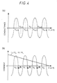
- Figure 4a shows the conductance difference as a function of voltage or equivalently as a function of energy.
- the voltage in the horizontal axis represents a gate voltage applied to gates GT1 and GT2 of Figure 1.
- the amplititude of the oscillation in the value of the conductance difference is less than the quantised conductance 2e 2 /h per 2DEG layer.
- V n indicates the voltage where the Fermi level coincides with the nth energy level.
- FIG. 4b this illustrates four-state logic operation using the device, when connected to a series resistor R L .
- the resistor R L may be connected to terminal D shown in Figure 1.
- the resistance is loaded with a voltage V L (as will be explained in more detail hereinafter).
- the graph shown in Figure 4b illustrates how the device can be used for four-state logic operation with four stable operation voltage points V0 to V1. With the application of a positive or negative voltage pulse having an absolute value higher than (V n -V n-1 )/2, the circuit is switched between V n-1 and V n . Whilst a four-state device is described, it will be appreciated that a different degree of multiplicity can be set by appropriately choosing V L and R L .
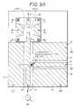
- FIG. 5 shows a 4-voltage state device used for logic operation.
- the CAPC corresponds to that shown in Figures 1 and 2, and corresponding parts are marked with the same reference numerals.
- Voltage sources V A , V G1 , V G2 , V T are connected as shown to the terminals A, G 2 , C, G 1 , and G T1 , G T2 respectively.
- An input to the device is V I (t) is applied at terminal 17 through a capacitor Cl to the gates G T1 , G T2 .
- An output from the device is taken through a load resistor R L that is biased by a load voltage V L , the output being derived at terminal 18.
- the gate voltages V G1 and V G2 applied to G 1 and G 2 are -0.9V and that applied to G T1 and G T2 is -0.5V.
- a voltage pulse V I (t) is superimposed on V T through the input terminal 17 so as to trigger a change between the stable voltage states V n and V n-1 .
- V A , V L and V C In order to achieve the 4-state condition illustrated in Figure 4b, special consideration needs to be given to the relative values of V A , V L and V C and the following condition needs to be established V A ⁇ V L ⁇ V C Generally, under these conditions, the device operates such that current flows from terminal A to either terminal D or terminal C. The characteristics to current flow for the two paths is substantially the same.
- FIG. 7a Four-state flip-flop-like digital operation of this device is demonstrated in Figure 7a.
- V I (t) consists of a number of trigger pulses that, as previously described, trigger the circuit between four different stable states.
- the input waveform can switch from a median operating level V OP to an upper level V U or a lower level V D .
- the input voltage includes three successive positive going pulses 19,20,21 followed by three negative going pulses 22,23,24.
- Pulse 19 causes the output 18 to flip from voltage V 0 to V 1 .
- pulse 20 causes the output voltage to flip from stable state V 1 to V 2 .
- pulse 21 causes a change to stable state V 3 .
- the negative going pulses 22,23,24 produce an inverse effect, so as to switch the stable state of the output 18 downwardly between the stable voltage levels.
- the input voltage need not necessarily be applied to the gates G T1 and G T2 . Instead, it could be superimposed on the voltage at terminal D.
- the operation time scale for the device needs to be longer than the electron time of flight from terminals A to C or D. This will be of the order to a few ps and so the operation time scale can be of the order of 10ps.
- the invention can also be used as a memory device and an example is illustrated in Figure 6.
- FIG. 6 The nomenclature of Figure 6 corresponds to that of Figure 5 and the device conditions and structures are all the same except that the input V I (t) is applied directly to terminal D and the current flowing in the output resistor R L is converted into an output voltage for example by means of a comparator A1.
- the result of memory operation for this device is shown in Figure 7b.
- the input voltage V I (t) is switched from an operating level VOP to either an upper "on” voltage V ON or a lower “off” voltage V OFF .
- the operating voltage V OP coincides with one of the four stable voltage points V n .
- the on-off voltage should lie between 0.5 (V n -V n-1 ) and 1.0 (V n -V n-1 ).
- a pulse from V OP to V ON switches the current flowing in resistor R L from a current I ON to I OFF , whereas the corresponding pulse from V OP to V OFF produces a reverse switching of the output load current from the I OFF to I ON , thereby producing a memory operation.
- the memory operation can take place at the four stable voltage levels V n shown in Figure 4.
- Figure 8 illustrates a signal processing device.
- the same nomenclature is used as in the preceding Figures.
- Two input voltage pulse trains V IA (t) and V IT (t) are superimposed respectively on DC voltage V A and V T , at input terminals 17A, 17T.
- Outputs are taken from terminals D and C, amplified by amplifiers A D and A C , the outputs of which are combined by output amplifier A O to provide an output at terminal 18.
- This device can be used for the following purposes:
- the device works as an amplifier.
- a small change to the input produces a large change at the output 18 according to the conductance characteristics shown in Figure 4.
- the slope of the curve shown in Figure 4a in the region of one of the stable voltage levels Vn, is used as the transfer function for the amplifier.
- An input signal applied to terminal 17A undergoes amplitude modulation through conductance modulation produced by a modulation voltage applied to input 17T.
- an oscillator can be constructed.
- the voltage V T is controlled, for example by an appropriate input at terminal 17T, the oscillation can be switched on and off and hence an oscillator including an amplitude modulator is fabricated.
- the voltage V T can be alternately biased on and off or, if an input is applied at 17T, it can be made to alternate between adjacent conductance peak and valleys shown in Figure 4a in order to achieve appropriate modulation.
- FIG. 9 yet another embodiment of the invention is shown wherein the device is integrated into a high-speed photoconductive switch.
- the device is formed in a substrate which has the same general structure as that shown in Figure 2, with a CAQPC device, referenced generally at 20, which is of the same construction as described with reference to Figure 1, with electrical connections (not shown) corresponding to those described with reference to Figure 5.
- the substrate additionally includes overlying electrodes 21,22,23,24,25, formed in the same way as electrodes G 1 and G 2 , spaced by non-conductive gaps 26,27. A further pair of non-conductive gaps 28,29 are similarly formed, on either side of electrode 24.
- An ultra-fast photoconductive switch or PCS 30 is formed at the junction of electrodes 22 and 24.
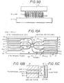
- the PCS 30 is shown in more detail in Figure 9b and consists of two sets of interdigitated fingers 31a,31b formed from the electrode material 22,24 overlying LT GaAs so as to provide an interdigitated metal-semiconductor-metal switch.
- An example of such an arrangement is described in more detail in J. Allam, K. Ogawa, J. White, N. deB. Baynes J.R.A. Cleaver, I. Ohbu, T. Tanoue and T. Mishima, Ultrafast Electronics and Optoelectronics Conf., 1993. Briefly, the recombination centres in the LTGaAs accelerate decay of photo-injected carriers and a high speed response of the switch is thereby realised.
- the result of incident photons is to produce a modulation on the electrode 22, which thereby modulates the voltage applied to gate G T2 of the CAQPC 20, which produces switching or alteration of the asymmetric wave function, in the manner previously described.
- the PCS switch 30 can be used to produce logical switching between multiple voltage levels as previously described or alternatively, the device can be used to produce modulation in a manner generally described with reference to Figure 8.
- All of the devices disclosed herein can be integrated with such high-speed photo-conductive switches and operated in the picosecond time domain. Such devices can be utilised as optoelectronic logical modulation devices within a network of such optically interconnected systems.
- the device is fabricated in the same general way as described with reference to Figure 9 and the device includes an array of PCS's 30a-h, each connected to one of the terminals of the CAQPC 20 by a respective transmission line 32.
- the PCS 30h in more detail, it consists of two sets of interdigitated electrodes as described with reference to Figure 9.
- the transmission line 32 formed in the same manner as transmission line 22 of Figure 9, extends from the gate region G T2 of the device 20, to a contact pad 33 at the edge of the substrate.
- the transmission line 32h is provided with a first set of interdigitated electrodes, in the manner shown in Figure 9 and the other interdigitated electrode set is coupled to transmission line 34 that extends to contact pad 35 at the edge of the substrate.
- the transmission line 32 is formed by selective etching of a conductive ground plane 36 to form parallel non-conducting gaps 37, 38 on opposite sides of the transmission line.
- Transmission line 34 is formed in a similar way. In use, a potential difference is applied to the contacts 33, 35, and when photons are incident upon the PCS 30h, an ultrafast electrical pulse is induced, which travels along the transmission line 32 to the gate G T2 of the CAQPC 20.
- Each of the other PCS's 30 is coupled in a similar manner to one of the inputs of the device 20, as can be seen in more detail in Figure 11.
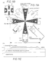
- FIG 11a the connections to the device 20 are shown in more detail, in plan view.
- the device 20, shown in Figure llb is essentially the same as that shown in Figure 1 and has its corresponding connections A-D, G T1 , G T2 , G 1 , G 2 connected to a respective one of the transmission lines 32a-32h shown in Figure 10.
- Two of the connections are shown in more detail in Figure lla, for gate electrode G T2 and connection C respectively.
- the transmission line 32h it is connected to a tapered conductive portion 39 which connects to the gate electrode G T2 shown in Figure llb.
- this is connected to an ohmic contact 40 which is connected to the 2DEG regions 9 ( Figure 2) in QPC2 ( Figure 1).
- the layers 5-12 are configured as a mesa, shown by outline 41 in Figure lla, which overlies the LTGaAs photoconductive layer 4 on the substrate 3. Corresponding connections are made to the other gates and channels of the device 20.
- photons incident on the PCS's 30a-h can be used to trigger the multiple logic levels exhibited by the device 20 so that the device is switched between a number of multiple voltage output levels, dependent upon the number of trigger pulses produced by the various photoconductive switches 30.
- the output of the device can be detected as described previously with reference to Figure 5, so as to provide a highly integrated, multiple level logic output system with a high degree of integration.
- CAQDs coupled asymmetric quantum dots
- quantum dots tend to constrain small numbers of electrons in a quantum well (in theory, single electrons can be constrained in this way) and as a result, CAQDs demonstrate a higher peak to valley ratio in their conductance or current-voltage characteristics (see Figure 4) but a lower current level because of the higher degree of wavefunction confinement in the quantum dots.
- Figure 12 illustrates a CAQD manufactured by the same techniques described with reference to Figures 1 and 2.
- the electrodes G 1 and G 2 are however each shaped in such a way as to provide an electron confinement region 42, 43 defining quatum dots QD1, QD2.
- Each QD has narrow conduction channels at both ends (CW 1 for example), which channels act as tunnelling barriers and confine strongly electron wave functions into the QDs.
- Two dimensional electron gas and the electrode structures are also available in In 1-x Ga x As y P 1-y /InP and Si 1-x Ge x /Si 1-y Ge y heterojunction interface layers and in Si/SiO 2 inversion layer.
- the CAQPCs and CAQDs described hereinbefore are fabricated by means of split-gate processing with electron-beam lithography and metalisation.
- other methods could be used.
- focussed ion-beam implantation can be used to form the electrode structure shown in Figures 1 and 12.
- a side-gate formation process can be used in which electron beam lithography, followed by chemical etching, can realise side-gate electrode structures for defining the region with an asymmetric quantum mechanical wave function.
Landscapes
- Engineering & Computer Science (AREA)
- Chemical & Material Sciences (AREA)
- Nanotechnology (AREA)
- Physics & Mathematics (AREA)
- Mathematical Physics (AREA)
- Theoretical Computer Science (AREA)
- Crystallography & Structural Chemistry (AREA)
- Junction Field-Effect Transistors (AREA)
Claims (19)
- Dispositif électronique ayant trois ou plus de trois états, comportant :un moyen destiné à définir une configuration de puits quantiques comprenant des première et seconde régions de puits quantiques (QPC1, 2 ; QD1, 2) en des emplacements spatialement différents ;des moyens (G1, G2, GT1, GT2) destinés à établir une fonction d'onde ψn (x) de porteurs de charges de mécanique quantique spatialement asymétrique définissant trois ou plus de trois niveaux d'énergie quantifiés stables dans la configuration de puits quantiques, des niveaux stables apparaissant dans certaines, différentes, des régions de puits quantiques ;des moyens de commande (A, B, C, D, G1, G2, GT1, GT2) destinés à amener une charge dans la configuration de puits à prendre certains, différents, desdits trois ou plus de trois niveaux quantifiés ; etdes moyens de sortie (18) qui, en réponse auxdits emplacements différents desdits niveaux stables, sont destinés à définir trois ou plus de trois conditions logiques de sortie, chaque région de puits quantiques comprenant des moyens à électrodes de grille (G1, G2, GT1, GT2) définissant des régions (W1, W2) de confinement de porteurs de charges, et en outre des moyens à électrodes de grille (GT1, GT2) pouvant fonctionner de façon à séparer les régions de confinement pour établir la fonction d'onde asymétrique à travers lesdites régions de confinement.
- Dispositif selon la revendication 1, comprenant un substrat (3), des moyens (9, 13, G1, G2, GT1, GT2) sur le substrat pour produire la configuration de puits quantiques dans laquelle ladite fonction d'onde est établie, des moyens à sources (A, B) pour des porteurs devant être fournis à la configuration de puits, et des moyens à drains (C, D) pour des porteurs provenant de la configuration de puits.
- Dispositif selon la revendication 1 ou 2, dans lequel chaque région de puits quantiques comprend un contact ponctuel quantique (QPC1, QPC2).
- Dispositif selon la revendication 1 ou 2, dans lequel lesdites régions de puits quantiques sont configurées sous la forme de points quantiques (QD1, QD2).
- Dispositif selon la revendication 3, dans lequel chaque contact ponctuel quantique comprend un gaz d'électrons essentiellement à deux dimensions (9a, b) s'étendant entre la source et le drain à travers leurs régions de confinement.
- Dispositif selon l'une quelconque des revendications précédentes, comprenant des moyens d'entrée (17) destinés à appliquer une impulsion de déclenchement d'entrée (VI(t)) pour amener le dispositif à prendre un niveau d'énergie dans lequel la fonction d'onde de mécanique quantique prend un état tel qu'une conduction apparaít préférentiellement dans l'une, particulière, desdites régions de confinement.
- Dispositif selon la revendication 6, comprenant une résistance de charge (RL) connectée à l'un desdits drains, des moyens destinés à appliquer une tension de charge (VL) à ladite résistance de charge, et des moyens de sortie (18) sensibles à la tension développée audit drain (D), de manière que ladite impulsion d'entrée commute séquentiellement ladite sortie entre trois ou plus de trois niveaux logiques.
- Dispositif selon la revendication 7, comprenant des moyens de sortie (A1) sensibles à la tension développée à travers ladite résistance de sortie (RL) et des moyens d'entrée (VI(t)) destinés à appliquer une impulsion d'entrée audit drain (D), de manière à produire une fonction de mémoire.
- Dispositif selon l'une quelconque des revendications précédentes, comprenant des moyens de sortie (AC, AD, AO) destinés à contrôler la différence de conductance entre lesdites première et seconde régions de puits quantiques.
- Dispositif selon l'une quelconque des revendications 2 à 8, fonctionnant à la manière d'un modulateur, comprenant des moyens d'entrée (17T) destinés à moduler une tension (VIA) appliquée au dispositif de façon à moduler le courant développé à au moins l'un desdits moyens de drains.
- Dispositif selon la revendication 10, dans lequel ladite tension (VIA) est connectée auxdits moyens à sources (A).
- Dispositif selon la revendication 10 ou 11, dans lequel lesdits moyens d'entrée (17T) sont connectés auxdits moyens de commande (GT1, GT2).
- Dispositif selon l'une quelconque des revendications précédentes, configuré de façon à fonctionner à la manière d'un amplificateur.
- Dispositif selon l'une quelconque des revendications 1 à 12, configuré de façon à fonctionner à la manière d'un oscillateur.
- Dispositif selon l'une quelconque des revendications 1 à 12, connecté à un commutateur photoconducteur.
- Dispositif selon la revendication 15, dans lequel le commutateur photoconducteur comprend une couche photosensible (4), et des premier et second jeux d'électrodes interdigitées (31a, b) qui recouvrent la couche photosensible.
- Dispositif selon la revendication 16, dans lequel la couche photosensible est formée d'une matière du type LT GaAs.
- Dispositif selon l'une quelconque des revendications 15 à 17 et un groupement de commutateurs photosensibles (30a-h) connectés chacun à une borne respective du dispositif.
- Dispositif selon la revendication 18, comprenant des lignes de transmission (32a-h) connectant les commutateurs respectivement aux bornes du dispositif.
Applications Claiming Priority (2)
| Application Number | Priority Date | Filing Date | Title |
|---|---|---|---|
| GB9311111 | 1993-05-28 | ||
| GB939311111A GB9311111D0 (en) | 1993-05-28 | 1993-05-28 | Quantum structure devices |
Publications (3)
| Publication Number | Publication Date |
|---|---|
| EP0626730A2 EP0626730A2 (fr) | 1994-11-30 |
| EP0626730A3 EP0626730A3 (fr) | 1995-06-21 |
| EP0626730B1 true EP0626730B1 (fr) | 2001-07-04 |
Family
ID=10736327
Family Applications (1)
| Application Number | Title | Priority Date | Filing Date |
|---|---|---|---|
| EP94303174A Expired - Lifetime EP0626730B1 (fr) | 1993-05-28 | 1994-04-29 | Dispositif semi-conducteur fabriqué à échelle nanométrique |
Country Status (4)
| Country | Link |
|---|---|
| US (1) | US5485018A (fr) |
| EP (1) | EP0626730B1 (fr) |
| DE (1) | DE69427617T2 (fr) |
| GB (1) | GB9311111D0 (fr) |
Families Citing this family (17)
| Publication number | Priority date | Publication date | Assignee | Title |
|---|---|---|---|---|
| KR100199024B1 (ko) * | 1995-12-22 | 1999-06-15 | 정선종 | 두개의 비대칭 양자점을 갖는 평면 공명관통 트랜지스터 |
| GB2314674B (en) * | 1996-06-27 | 1998-09-16 | Toshiba Cambridge Res Center | Optically operable semiconductor device |
| GB2314673B (en) * | 1996-06-27 | 1998-12-30 | Toshiba Cambridge Res Center | Semiconductor device |
| US5939764A (en) * | 1997-04-23 | 1999-08-17 | President And Fellows Of Harvard College | Direct current voltage transformer |
| WO1998049587A1 (fr) * | 1997-05-01 | 1998-11-05 | Trustees Of The Stevens Institute Of Technology | Procede et appareil de modulation de plasmons guides |
| US6541803B1 (en) * | 2000-04-21 | 2003-04-01 | The United States Of America As Represented By The Secretary Of The Army | High-speed high electron mobility transistor photodetector using low temperature gallium arsenide |
| DE10042663A1 (de) * | 2000-08-31 | 2002-03-14 | Deutsche Telekom Ag | Eletronenspektrometer |
| TW514968B (en) * | 2000-09-01 | 2002-12-21 | Btg Int Ltd | Nanoelectronic devices, circuits including such devices and methods for achieving transistor action and rectifying an alternating voltage in such device |
| EP1187219A1 (fr) * | 2000-09-01 | 2002-03-13 | Btg International Limited | Dispositifs électroniques ballistiques |
| US6403990B1 (en) * | 2001-03-27 | 2002-06-11 | Agilent Technologies, Inc. | Short turn-off time photoconductive switch |
| GB0109782D0 (en) * | 2001-04-20 | 2001-06-13 | Btg Int Ltd | Nanoelectronic devices and circuits |
| RU2388111C1 (ru) * | 2009-03-25 | 2010-04-27 | Учреждение Российской академии наук Физический институт им. П.Н. Лебедева РАН | Элемент троичной логики |
| CN102176521B (zh) * | 2010-12-08 | 2013-08-07 | 南京邮电大学 | 太赫兹表面等离子体波温度控制开关及其控制方法 |
| WO2013027712A1 (fr) * | 2011-08-22 | 2013-02-28 | 独立行政法人科学技術振興機構 | Dispositif de redressement, transistor et procédé de redressement |
| US8907378B2 (en) * | 2013-03-15 | 2014-12-09 | Mitsubishi Electric Research Laboratories, Inc. | High electron mobility transistor with multiple channels |
| US9991370B2 (en) * | 2014-12-15 | 2018-06-05 | The Royal Institution For The Advancement Of Learning/Mcgill University | Methods and systems for ultra-high quality gated hybrid devices and sensors |
| US11355624B2 (en) * | 2019-04-05 | 2022-06-07 | Stmicroelectronics S.R.L. | Electrically confined ballistic devices and methods |
Citations (2)
| Publication number | Priority date | Publication date | Assignee | Title |
|---|---|---|---|---|
| JPH0437069A (ja) * | 1990-06-01 | 1992-02-07 | Hitachi Ltd | 共鳴トンネリング素子及びそれを用いた可変コンダクタンス回路 |
| JPH04125966A (ja) * | 1990-09-17 | 1992-04-27 | Nec Corp | 半導体装置およびその製造方法 |
Family Cites Families (13)
| Publication number | Priority date | Publication date | Assignee | Title |
|---|---|---|---|---|
| US5138408A (en) * | 1988-04-15 | 1992-08-11 | Nec Corporation | Resonant tunneling hot carrier transistor |
| US4825872A (en) * | 1988-08-05 | 1989-05-02 | Critikon, Inc. | Finger sensor for pulse oximetry system |
| EP0394757B1 (fr) * | 1989-04-27 | 1998-10-07 | Max-Planck-Gesellschaft zur Förderung der Wissenschaften e.V. | Structure semi-conductrice avec une couche à porteur de charge bidimensionelle et méthode de fabrication |
| US5105232A (en) * | 1989-09-26 | 1992-04-14 | Massachusetts Institute Of Technology | Quantum field-effect directional coupler |
| DE4020813A1 (de) * | 1990-01-23 | 1991-07-25 | Max Planck Gesellschaft | Elektronenwellen-gekoppeltes halbleiter-schaltelement |
| US5051791A (en) * | 1990-03-12 | 1991-09-24 | At&T Bell Laboratories | Apparatus comprising refractive means for elections |
| GB2256313B (en) * | 1991-01-04 | 1995-03-29 | Hitachi Europ Ltd | Semiconductor device |
| EP0517647A3 (en) * | 1991-06-04 | 1993-07-21 | Fujitsu Limited | Quantum semiconductor device that uses a quantum point contact for producing a quantum mechanical carrier wave with directivity |
| GB2261989B (en) * | 1991-11-27 | 1995-07-12 | Hitachi Europ Ltd | Switching device |
| US5283445A (en) * | 1991-11-29 | 1994-02-01 | Fujitsu Limited | Quantum semiconductor device employing quantum boxes for enabling compact size and high-speed operation |
| GB9125727D0 (en) * | 1991-12-03 | 1992-01-29 | Hitachi Europ Ltd | Non-linear optical device |
| JP2701633B2 (ja) * | 1991-12-09 | 1998-01-21 | 日本電気株式会社 | 半導体装置 |
| GB9206149D0 (en) * | 1992-03-19 | 1992-05-06 | Hitachi Europ Ltd | Charge carrier flow control device |
-
1993
- 1993-05-28 GB GB939311111A patent/GB9311111D0/en active Pending
-
1994
- 1994-04-29 DE DE69427617T patent/DE69427617T2/de not_active Expired - Fee Related
- 1994-04-29 EP EP94303174A patent/EP0626730B1/fr not_active Expired - Lifetime
- 1994-05-27 US US08/250,262 patent/US5485018A/en not_active Expired - Fee Related
Patent Citations (2)
| Publication number | Priority date | Publication date | Assignee | Title |
|---|---|---|---|---|
| JPH0437069A (ja) * | 1990-06-01 | 1992-02-07 | Hitachi Ltd | 共鳴トンネリング素子及びそれを用いた可変コンダクタンス回路 |
| JPH04125966A (ja) * | 1990-09-17 | 1992-04-27 | Nec Corp | 半導体装置およびその製造方法 |
Non-Patent Citations (1)
| Title |
|---|
| High Speed Semiconducting Devices, Ch.8 Ed. S.M.Sze Pub. J.Wiley, 1990 * |
Also Published As
| Publication number | Publication date |
|---|---|
| EP0626730A3 (fr) | 1995-06-21 |
| DE69427617D1 (de) | 2001-08-09 |
| EP0626730A2 (fr) | 1994-11-30 |
| GB9311111D0 (en) | 1993-07-14 |
| DE69427617T2 (de) | 2002-05-08 |
| US5485018A (en) | 1996-01-16 |
Similar Documents
| Publication | Publication Date | Title |
|---|---|---|
| US5485018A (en) | Nanofabricated device for multiple-state logic operation | |
| JP3745015B2 (ja) | 電子デバイス | |
| US4912531A (en) | Three-terminal quantum device | |
| US4581621A (en) | Quantum device output switch | |
| US4575924A (en) | Process for fabricating quantum-well devices utilizing etch and refill techniques | |
| US5989947A (en) | Method for the manufacture of quantum structures, in particular quantum dots and tunnel barriers as well as components with such quantum structures | |
| JP3194941B2 (ja) | 半導体装置 | |
| US4833511A (en) | Phototransistor device | |
| US4777516A (en) | Monolithic integration of light emitting elements and driver electronics | |
| US5932889A (en) | Semiconductor device with floating quantum box | |
| KR100533293B1 (ko) | 양자소자 | |
| US5032877A (en) | Quantum-coupled ROM | |
| US4783427A (en) | Process for fabricating quantum-well devices | |
| US4799091A (en) | Quantum device output switch | |
| US5701017A (en) | Semiconductor device and method for its manufacture | |
| JPH073822B2 (ja) | 共鳴トンネリング半導体デバイス | |
| US5621222A (en) | Superlattice semiconductor device | |
| JPS63316484A (ja) | 量子効果半導体装置 | |
| US4969018A (en) | Quantum-well logic using self-generated potentials | |
| GB2270590A (en) | Semiconductor devices including field effect transistors | |
| EP0186301B1 (fr) | Dispositif semi-conducteur à grande vitesse | |
| JP2001156298A (ja) | 半導体素子 | |
| JPH0740570B2 (ja) | 共鳴トンネリング装置 | |
| US5512764A (en) | Coupled-quantum-well field-effect resonant tunneling transistor for multi-valued logic/memory applications | |
| D'Asaro et al. | Batch fabrication and structure of integrated GaAs-Al/sub x/Ga/sub 1-x/As field-effect transistor-self-electro-optic effect devices (FET-SEED's) |
Legal Events
| Date | Code | Title | Description |
|---|---|---|---|
| PUAI | Public reference made under article 153(3) epc to a published international application that has entered the european phase |
Free format text: ORIGINAL CODE: 0009012 |
|
| AK | Designated contracting states |
Kind code of ref document: A2 Designated state(s): DE FR GB IT NL |
|
| PUAL | Search report despatched |
Free format text: ORIGINAL CODE: 0009013 |
|
| AK | Designated contracting states |
Kind code of ref document: A3 Designated state(s): DE FR GB IT NL |
|
| 17P | Request for examination filed |
Effective date: 19951020 |
|
| 17Q | First examination report despatched |
Effective date: 19960925 |
|
| GRAG | Despatch of communication of intention to grant |
Free format text: ORIGINAL CODE: EPIDOS AGRA |
|
| GRAG | Despatch of communication of intention to grant |
Free format text: ORIGINAL CODE: EPIDOS AGRA |
|
| GRAH | Despatch of communication of intention to grant a patent |
Free format text: ORIGINAL CODE: EPIDOS IGRA |
|
| RIC1 | Information provided on ipc code assigned before grant |
Free format text: 7H 01L 29/76 A, 7H 01L 29/12 B |
|
| GRAH | Despatch of communication of intention to grant a patent |
Free format text: ORIGINAL CODE: EPIDOS IGRA |
|
| GRAA | (expected) grant |
Free format text: ORIGINAL CODE: 0009210 |
|
| AK | Designated contracting states |
Kind code of ref document: B1 Designated state(s): DE FR GB IT NL |
|
| PG25 | Lapsed in a contracting state [announced via postgrant information from national office to epo] |
Ref country code: IT Free format text: LAPSE BECAUSE OF FAILURE TO SUBMIT A TRANSLATION OF THE DESCRIPTION OR TO PAY THE FEE WITHIN THE PRE;WARNING: LAPSES OF ITALIAN PATENTS WITH EFFECTIVE DATE BEFORE 2007 MAY HAVE OCCURRED AT ANY TIME BEFORE 2007. THE CORRECT EFFECTIVE DATE MAY BE DIFFERENT FROM THE ONE RECORDED.SCRIBED TIME-LIMIT Effective date: 20010704 Ref country code: FR Free format text: LAPSE BECAUSE OF FAILURE TO SUBMIT A TRANSLATION OF THE DESCRIPTION OR TO PAY THE FEE WITHIN THE PRESCRIBED TIME-LIMIT Effective date: 20010704 |
|
| REF | Corresponds to: |
Ref document number: 69427617 Country of ref document: DE Date of ref document: 20010809 |
|
| EN | Fr: translation not filed | ||
| REG | Reference to a national code |
Ref country code: GB Ref legal event code: IF02 |
|
| PLBE | No opposition filed within time limit |
Free format text: ORIGINAL CODE: 0009261 |
|
| STAA | Information on the status of an ep patent application or granted ep patent |
Free format text: STATUS: NO OPPOSITION FILED WITHIN TIME LIMIT |
|
| 26N | No opposition filed | ||
| PGFP | Annual fee paid to national office [announced via postgrant information from national office to epo] |
Ref country code: NL Payment date: 20040429 Year of fee payment: 11 |
|
| PGFP | Annual fee paid to national office [announced via postgrant information from national office to epo] |
Ref country code: DE Payment date: 20040630 Year of fee payment: 11 |
|
| PGFP | Annual fee paid to national office [announced via postgrant information from national office to epo] |
Ref country code: GB Payment date: 20050415 Year of fee payment: 12 |
|
| PG25 | Lapsed in a contracting state [announced via postgrant information from national office to epo] |
Ref country code: NL Free format text: LAPSE BECAUSE OF NON-PAYMENT OF DUE FEES Effective date: 20051101 Ref country code: DE Free format text: LAPSE BECAUSE OF NON-PAYMENT OF DUE FEES Effective date: 20051101 |
|
| NLV4 | Nl: lapsed or anulled due to non-payment of the annual fee |
Effective date: 20051101 |
|
| PG25 | Lapsed in a contracting state [announced via postgrant information from national office to epo] |
Ref country code: GB Free format text: LAPSE BECAUSE OF NON-PAYMENT OF DUE FEES Effective date: 20060429 |
|
| GBPC | Gb: european patent ceased through non-payment of renewal fee |
Effective date: 20060429 |