EP0627748A2 - Flachkabel - Google Patents
Flachkabel Download PDFInfo
- Publication number
- EP0627748A2 EP0627748A2 EP93304227A EP93304227A EP0627748A2 EP 0627748 A2 EP0627748 A2 EP 0627748A2 EP 93304227 A EP93304227 A EP 93304227A EP 93304227 A EP93304227 A EP 93304227A EP 0627748 A2 EP0627748 A2 EP 0627748A2
- Authority
- EP
- European Patent Office
- Prior art keywords
- substrate
- polymeric
- polymeric material
- conductor
- flat cable
- Prior art date
- Legal status (The legal status is an assumption and is not a legal conclusion. Google has not performed a legal analysis and makes no representation as to the accuracy of the status listed.)
- Granted
Links
Images


Classifications
-
- H—ELECTRICITY
- H01—ELECTRIC ELEMENTS
- H01B—CABLES; CONDUCTORS; INSULATORS; SELECTION OF MATERIALS FOR THEIR CONDUCTIVE, INSULATING OR DIELECTRIC PROPERTIES
- H01B7/00—Insulated conductors or cables characterised by their form
- H01B7/08—Flat or ribbon cables
- H01B7/0846—Parallel wires, fixed upon a support layer
-
- G—PHYSICS
- G02—OPTICS
- G02B—OPTICAL ELEMENTS, SYSTEMS OR APPARATUS
- G02B6/00—Light guides; Structural details of arrangements comprising light guides and other optical elements, e.g. couplings
- G02B6/44—Mechanical structures for providing tensile strength and external protection for fibres, e.g. optical transmission cables
- G02B6/4401—Optical cables
- G02B6/4403—Optical cables with ribbon structure
-
- G—PHYSICS
- G02—OPTICS
- G02B—OPTICAL ELEMENTS, SYSTEMS OR APPARATUS
- G02B6/00—Light guides; Structural details of arrangements comprising light guides and other optical elements, e.g. couplings
- G02B6/44—Mechanical structures for providing tensile strength and external protection for fibres, e.g. optical transmission cables
- G02B6/4479—Manufacturing methods of optical cables
- G02B6/448—Ribbon cables
Definitions
- This invention relates to flat cable and in particular flat cable comprising a plurality of conductors and a substrate comprising a polymeric material.
- Flat cables are well known and take several forms.
- a plurality of conductors are placed parallel to one another and laminated between a pair of films which surround each conductor thereby insulating each conductor from its neighbors as well as forming the flat cable construction.
- the insulation thickness of each individual conductor cannot always be controlled as precisely and reproducibly as desired.
- the film is generally of a polymeric material similar to that of the insulation and in order to achieve a bond between the insulated conductors and the film, the film must be heated to about its melting point. At these temperatures it is difficult to maintain the dimensions of the film and this can lead to improper alignment of the wires and even buckling and shrinking of the film. Further, it has been found that with certain polymeric materials it is difficult to separate an individual insulated conductor from the carrier film unless the bond strength is well controlled. If the bond is too strong, peeling will then destroy the carrier film or the conductor insulation. It is desirable to be able to peel the individual insulated conductors from the film as cleanly as possible.
- U.S. Patent No. 4,678,864 to Cox also discloses the use of a ground plane in the construction of a flat cable assembly.
- the ground plane is positioned between the flat cable and a plastic covering.
- the plastic covering is coated over a major portion of its surface with a release agent so that it can be readily separated from the cable.
- the ground plane itself is not bonded to the flat cable.
- the flat cable itself is of conventional structure comprising a supporting film and insulated wires and thus it would be difficult to peel individual insulated wires cleanly from the cable.
- Another object of this invention is to provide flat cables in which insulated conductors are bonded to carrier films of a thickness of less than 2.5 mil (98 microns) at a desired preselected spacing and also a method for providing such cables.
- Yet another object of this invention is to provide flat cables in which high melting insulations are bonded to high melting carrier films at a desired preselected spacing and also a method for providing such cables.
- This invention provides a flat cable having dimensional stability and consistent bond strength with good peelability of the constituent insulated conductors, that is the ability to readily and cleanly separate one or more of the individual conductors from a carrier film (polymeric substrate) more than 1 mil (39.4 microns) thick (thinner carrier films generally fail cohesively if separation is attempted).
- One aspect of this invention comprises a flat cable comprising:
- a second aspect of this invention comprises a flat cable having:
- a third aspect of this invention comprises a method of preparing a flat cable which comprises;
- a fourth aspect of the invention provides a flat cable produced by the method of the third aspect of the invention.
- a fifth aspect of this invention comprises a method of preparing a flat cable comprising a plurality of elongated conductive components each individually surrounded by a layer of first polymeric material that is bonded to a polymeric substrate and having a preselected bond strength thereto, which comprises:
- a sixth aspect of the invention provides a flat cable produced by the method of the fifth aspect of the invention.
- Fig. 1 illustrates a flat cable of this invention adhered to a support layer.
- Fig. 2 shows the support layer being peeled away from the polymer substrate of the flat cable.
- Fig. 3 illustrates a flat cable of this invention.
- Fig. 4 is a cross section of another cable of this invention in which a number of different types of conductors are bonded to the substrate.
- Fig. 5 illustrates a method for the manufacture of the flat cable of this invention.
- the flat cable of this invention comprises a plurality of conductors, each individually surrounded by a layer of a first polymeric material, bonded to a polymeric substrate.
- Fig. 1 illustrates a flat cable of this invention in which each conductor comprises an insulated electrical conductor.
- flat cable 10 comprises a polymeric substrate 12, peelably adhered to a support layer 16, and individually insulated conductors 14.
- the conductors are identical.
- Fig. 2 shows the support layer 16 being peeled away from the polymeric substrate 12.
- Fig. 3 shows the flat cable after removal of the support layer.
- the individual electrical conductors can be single or multiple stranded conductors.
- one or more of the conductors comprises a twisted pair. i.e. a pair of individually insulated conductors twisted together, a cable, i.e. one or more insulated conductors within an outer jacket, including coaxial cables in which one of the conductors surrounds an inner insulated conductor.
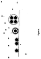
- flat cable 20 comprises substrate 21 which carries an insulated wire 22, a twisted pair of wires 23 and 24, a coaxial cable 25 comprising inner conductor 26, outer conductor 27 surrounded by jacket 28 and a cable 29 comprising four individual wires 30 surrounded by jacket 31.
- the conductor comprises an optical fiber surrounded with a layer of polymeric material (typically the jacket of a fiber optic cable).
- a layer of polymeric material typically the jacket of a fiber optic cable.
- the term conductor is used herein to encompass a variety of possible arrangements of electrical conductors as well as optical fiber cables or individual optical fibers surrounded with a protective polymeric material.
- the term insulated conductor is used herein to refer to any conductor or conductor arrangement surrounded by a layer of polymeric material.
- the conductor is surrounded with a layer of a first polymeric material.
- the conductor can be surrounded by additional layers of polymeric material as long as the outer most layer comprises the first polymeric material.
- the first polymeric material preferably has a melting point of at least 200°C and is preferably, for example, selected from ethylene-tetrafluoroethylene copolymers (including terpolymers), ethylene-trichlorofluoroethylene copolymers, polyethylene terephthalate, polybutylene terephthalate, polyamides, in particular, aromatic polyamides, polyimides, polyarylene ethers and the like.
- the first polymeric material may be crosslinked if desired to provide improved properties, particularly at elevated temperatures.
- the first polymeric material can be, for example, polyvinyl chloride, polyethylene terephthalate, polybutylene terephthalate, polyethylene, polyvinylidene fluoride, ethylene-tetrafluoroethylene copolymers (including terpolymers), ethylene-trichlorofluoroethylene copolymers, polyamides, in particular, aromatic polyamides, polyimides and the like.
- the first polymeric material may be crosslinked if desired to provide improved properties, particularly at elevated temperatures.
- the conductor is an electrical conductor which is insulated by at least one surrounding layer of a first polymer comprising an ethylene-tetrafluoroethylene copolymer.
- the insulated conductors are arranged parallel to one another and bonded to a polymeric substrate capable of bonding to the first polymeric material.
- the polymeric substrate comprises a second polymeric material capable of bonding to the first polymeric material that surrounds the conductors to be formed into the flat cable.
- the second polymeric material is of the same polymer as the first polymeric.
- Second polymeric materials for use in the polymeric substrate having a melting point of at least 200°C as described in the first aspect of the invention, are preferably selected, for example, from ethylene-tetrafluoroethylene copolymers (including terpolymers), ethylene-trichlorofluoroethylene copolymers, polyamides, in particular, aromatic polyamides, polyimides, polyarylene ethers and the like.
- the second polymer material is preferably at least partly crystalline and/or has a melting point of at least 225°C, more preferably a melting point of at least 240°C, most preferably a melting point of at least 260°C.
- the polymeric substrate in this first aspect of the invention is preferably from about 10 to about 200 microns thick, more preferably about 20 to about 150 microns. If the polymer is at least partly crystalline, the melting point is the crystalline melting point.
- Preferred second polymeric materials formed into a polymeric substrate having a thickness less than 2.5 mils (less than 98 microns), are, for example, polyvinyl chloride, polyethylene, polyethylene terephthalate, poly(butylene terephthalate), vinylidene fluoride homopolymers and copolymers, ethylene-tetrafluoroethylene copolymers (including terpolymers), ethylene-trichlorofluoroethylene copolymers, tetrafluoroethylene-perfluoroalkoxy vinyl ether copolymers, polyamides, in particular, aromatic polyamides, polyimides and the like.
- the polymeric substrate is preferably about 0.25 to about 2.4 mils thick (10 to 95 microns), for example, 0.25 to 2 mils (10 to 78 microns) thick, more preferably 0.25 to 1.5 mils (10 to 59 microns), for example, 0.5 to 1.0 mils (20 to 40 microns) thick.
- a particular advantage of flat cables bonded to polymeric substrates much less than 2.5 mils (much less than 98 microns) is that they can be curved in the plane of the flat cable (to form half "meanders") without having to fold the cable to equalize intra-conductor stresses because, in this thickness range, substrate stretching and distortion can accommodate the differing circumference of curvature between inner and outer conductors around the curve.
- cables with thin polymeric substrates can be "accordioned" transversely so as to fit into, for example, narrower channels or apertures and only spread out to their full width where they enter a connector.
- Substantially parallel means that a first conductor of a flat cable of the invention does not deviate from parallelism to an adjacent second conductor of the flat cable by more than 1% (percent) of the spacing therebetween.
- such substantial parallelism with substantial absence of sagging or buckling of the polymeric matrix is maintained along a length of flat cable of at least 24 inches (61 cm); more preferably such substantial parallelism with substantial absence of sagging or buckling of the polymeric matrix is maintained along a length of flat cable of at least 60 inches (152.4 cm); most preferably such substantial parallelism with substantial absence of sagging or buckling of the polymeric matrix is maintained along a length of flat cable of at least 120 inches (305 cm).
- such substantial parallelism with substantial absence of sagging or buckling of the polymeric matrix is maintained along a length of flat cable of at least 50 feet (1524 cm).
- a flat cable in accordance with the invention having a first and a second edge and comprising n parallel insulated conductors, where n is an integer ranging from 2 to 100, wherein a first conductor is the nearest conductor to the first edge of the cable and a nth conductor is the nearest to the second edge, the center to center spacing between any two adjacent conductive conductors of the flat cable and the cumulative spacing between a first conductor and a nth conductor is held to within 1% of the desired selected spacing therebetween along a length of flat cable equal to at least 24 inches (61 cm).
- the center to center spacing between any two adjacent conductive conductors of the flat cable and the cumulative spacing between a first conductor and a nth conductor is held to within 0.5% of the desired selected spacing therebetween. Most preferably the center to center spacing between any two adjacent conductive conductors of the flat cable and the cumulative spacing between a first conductor and a nth conductor is held to within 0.1% of the desired selected spacing therebetween. More preferably the desired spacing between any two adjacent conductive conductors of the flat cable and the cumulative spacing between a first conductor and a nth conductor is held to within a selected limit over a length of flat cable of at least 60 inches (152.4 cm). Most preferably the desired spacing between any two adjacent conductive conductors of the flat cable and the cumulative spacing between a first conductor and a nth conductor is held to within a selected limit over a length of flat cable of at least 50 feet (1524 cm).
- the support layer of the third (method) aspect of the invention is a material that is dimensionally stable at least at the temperature at which the first and second polymeric layers are heated so as to cause them to adhere together. Furthermore the adhesion between the support layer and the substrate film material must be sufficiently secure at the temperature at which the first and second polymeric layers are caused to adhere together that the bond therebetween remains integral such that the dimensions of the second polymeric layer remain substantially unchanged (except for thermal expansion effects) during the steps of heating one or both of, and contacting, the first and second polymeric layers. Moreover, the adhesion between the second polymeric layer and the support layer should be sufficient at all times during the process that the overall dimensions of the second polymeric layer remain substantially unaffected by performing the steps of the method of the invention.
- the temperature at which the first and second polymer materials are caused to adhere together is at least about the melting point of the lower melting material, more preferably at least about the ring and ball softening temperature of the lower melting material.
- the support layer of this aspect of the invention is any film of material dimensionally stable at least at the temperature at which the first and second polymeric layers are caused to adhere together.
- Preferred support layers comprise materials selected from high temperature polymers such as polyimide and metals such as aluminum, nickel, copper, iron and the like.
- the support layer may be peelably adhered to the polymeric substrate by melt bonding above the melting point of the polymeric substrate, extrusion lamination or by adhesive bonding with an adhesive layer or any combination thereof.
- Preferred adhesives are polyesters.
- a preferred polymeric substrate is a film of ethylenetetrafluoroethylene copolymer.
- Preferred support layers include thin films of aluminum or Kapton peelably adhered to the ethylene-tetrafluoroethylene copolymer film with a thin intervening layer of an adhesive, for example, a polyester (polyethylene terephthalate).
- an adhesive for example, a polyester (polyethylene terephthalate).
- the adhesive layer may adhere to one or both of the support layer and the polymeric substrate.
- the adhesive layer if used, adheres to the support layer more strongly than to the polymeric substrate so that both support and adhesive layers are peeled away together from the polymeric substrate.
- a support layer especially a metallic support layer
- an operator making flat cables is able, for the first time, to select a contact pressure between the insulated conductors and the polymeric substrate at a particular bonding temperature and consistently and reproducibly obtain thereby a desired bond strength between the conductors and the substrate.
- Such consistent, reproducible and selectable bond strengths are highly desirable, especially if the cables are to be used in automated terminating and cable handling equipment.
- the fifth aspect of the invention describes and defines with particularity how a cable, having these desirable characteristics, may be obtained.
- the operator determines the appropriate bonding temperature and pressure to obtain the desired bond strength by routine experimentation, for example by contacting the insulated conductor and polymeric substrate at a selection of pressures at a desired temperature or by varying the temperature at a desired contact pressure, then cooling the experimental assembly and measuring the bond strength. In most instances it will be advantageous to carry out the experimentation using the production bonding equipment. Once these operating parameters have been established the operator can then set the requisite temperatures and pressures, confident that the bonding process will operate to produce a flat cable having consistent bond strengths both between and within individual runs.
- Flat cables of the invention are preferably assembled by arranging the conductors in the desired parallel relationship. Adjacent insulated conductors can be touching each other or spaced apart from each other, as desired.
- the substrate and/or the conductors are heated to about the melting point of the impregnating second polymeric material just prior to bringing the conductors and substrate into contact.
- the insulated conductors are then placed into contact with a face of the polymeric substrate opposite to that which is adhered to the support layer. Sufficient pressure is applied to effect bonding with the desired bond strength. The amount of pressure applied should be about 1 to about 40 psi, preferably about 5 to about 20 psi.
- the assembly is then permitted to cool. Once the flat cable has cooled to the extent that the polymeric substrate, the insulation around the conductors and the bond therebetween have sufficient strength to resist permanent deformation, the support layer may be removed (peeled away) from the polymeric substrate.
- provision of a peelable metal support layer in one preferred embodiment of the method of the invention enables good temperature uniformity to be maintained across the conductors and polymeric substrate during the heating step prior to contact therebetween. Thus temperature control is facilitated and the temperature of the heating means may be reduced if desired.
- a metal support substrate and/or thinner polymeric substrates of the invention more rapid cooling of the adhered assembly is facilitated, reducing the tendency of some polymeric substrates to be embrittled in the flat cable.
- the polymeric substrate used in this example is a 2 mil film of an ethylene-tetrafluoroethylene (ETFE) copolymer, TefzelTM 280, 3 inches wide, pre-laminated to a 1 mil aluminum foil support layer by a low bond strength adhesive.
- the substrate and support layer together weigh 4.42 oz. per square yard with a total thickness of 3.25 mils.
- the following bonding procedure is carried out using the equipment shown in Fig. 5.
- the substrate 40 is paid off from a spool 41 and wound around roller 42 with the polymeric substrate film side facing toward the hot air blowers 43 and 44 where it is heated to its melting point.
- the substrate is then brought in contact with 20 MIL-W-84585/5-24 primary wires arranged horizontally in a single layer 44.
- the bonding is achieved by passing the heated substrate and the wires between rollers 42 and 46 where the Polymeric substrate layer is fused to the wires under an applied pressure of approximately 20 psi.
- the laminate is then wound around roller 48, and through a set of wire guides 49 and 50 to the caterpillar take up 51.
- the aluminum foil 52 is peeled off and discarded by a take up spool 53.
- Excess polymeric substrate film on both sides of the flat cable is trimmed off with an in-line slitter 54.
- the finished flat cable has a 2 mil ETFE copolymer film backing which still exhibits a tear strength of 2 lbs when tested in accordance with ASTM-D-1004.
- Example 1 is repeated using as the polymeric substrate for the flat cable a 0.5 mil Tefzel 280 film pre-laminated to a 1 mil KaptonTM film support layer.
- the total substrate weighs 1.65 oz. per square yard with a thickness of 1.5 mils.
- the bonding operation is carried out using the procedure and equipment as described in Example 1 with the 0.5 mil polymeric substrate layer being fused to a 2 inch wide set of 20 MIL-W-84585/5-24 wires.
- the support layer (Kapton film) 52 is then peeled off and discarded by a take up spool 53. Excess polymeric substrate film on both sides of the bonded cable is trimmed off with an in-line slitter 54.
- the finished flat cable is very flexible and has a 0.5 mil Tefzel film backing.
- Example 1 illustrates how the peel strength of the insulated conductor from the film may be controlled reproducibly by selecting different bonding pressures.
- Example 1 is repeated using as the polymeric substrate for the flat cable a 5 mil Tefzel 280 film pre-laminated to a 1 mil aluminum foil by a low bond strength adhesive.
- the bonding pressure is set by varying the pressure applied to the insulated conductors and polymeric substrate between, for example, rollers 42 and 46 of Figure 5.
- an applied pressure of 20 psi an average peel strength of about 0.4 lbs was consistently obtained between the insulated cables and the polymeric substrate, when tested in a 180° peel test in accordance with ASTM D903.
- ASTM D903 Average peel strengths of about 0.8 lbs and about 1.2 lbs respectively were consistently and reproducibly obtained.
Landscapes
- Physics & Mathematics (AREA)
- General Physics & Mathematics (AREA)
- Optics & Photonics (AREA)
- Engineering & Computer Science (AREA)
- Manufacturing & Machinery (AREA)
- Insulated Conductors (AREA)
Priority Applications (4)
| Application Number | Priority Date | Filing Date | Title |
|---|---|---|---|
| US07/890,045 US5327513A (en) | 1992-05-28 | 1992-05-28 | Flat cable |
| EP93304227A EP0627748B1 (de) | 1992-05-28 | 1993-06-01 | Flachkabel |
| AT93304227T ATE186609T1 (de) | 1993-06-01 | 1993-06-01 | Flachkabel |
| DE1993627000 DE69327000T2 (de) | 1993-06-01 | 1993-06-01 | Flachkabel |
Applications Claiming Priority (2)
| Application Number | Priority Date | Filing Date | Title |
|---|---|---|---|
| US07/890,045 US5327513A (en) | 1992-05-28 | 1992-05-28 | Flat cable |
| EP93304227A EP0627748B1 (de) | 1992-05-28 | 1993-06-01 | Flachkabel |
Publications (3)
| Publication Number | Publication Date |
|---|---|
| EP0627748A2 true EP0627748A2 (de) | 1994-12-07 |
| EP0627748A3 EP0627748A3 (de) | 1995-03-08 |
| EP0627748B1 EP0627748B1 (de) | 1999-11-10 |
Family
ID=26134317
Family Applications (1)
| Application Number | Title | Priority Date | Filing Date |
|---|---|---|---|
| EP93304227A Expired - Lifetime EP0627748B1 (de) | 1992-05-28 | 1993-06-01 | Flachkabel |
Country Status (2)
| Country | Link |
|---|---|
| US (1) | US5327513A (de) |
| EP (1) | EP0627748B1 (de) |
Families Citing this family (35)
| Publication number | Priority date | Publication date | Assignee | Title |
|---|---|---|---|---|
| JPH0794034A (ja) * | 1993-09-22 | 1995-04-07 | Fujitsu Ltd | フラットケーブル及びこれを用いたコネクタ付ケーブル |
| GB9404390D0 (en) * | 1994-03-07 | 1994-04-20 | Bicc Plc | Manufacture of electric cables |
| US5604834A (en) * | 1994-06-16 | 1997-02-18 | Sumitomo Electric Lightwave Corp. | Method of midspan and/or end entry to access selected optical fibers within an optical ribbon fiber |
| US5600750A (en) * | 1994-08-19 | 1997-02-04 | Sumitomo Electric Lightwave Corp. | Method for midspan entry of optical ribbon fiber |
| US6273977B1 (en) | 1995-04-13 | 2001-08-14 | Cable Design Technologies, Inc. | Method and apparatus for making thermally bonded electrical cable |
| US5727097A (en) * | 1996-06-07 | 1998-03-10 | Minnesota Mining And Manufacturing Company | Pull-proof fiber optic array connector |
| DE19625260A1 (de) * | 1996-06-25 | 1998-01-02 | Bosch Gmbh Robert | Faserbändchen für optische Breitband-Inhouse-Verkabelung |
| AU4173197A (en) * | 1996-10-18 | 1998-05-15 | W.L. Gore & Associates, Inc. | Microminiature planar signal transmission cable |
| US5902435A (en) * | 1996-12-31 | 1999-05-11 | Minnesota Mining And Manufacturing Company | Flexible optical circuit appliques |
| US6445866B1 (en) * | 1999-11-29 | 2002-09-03 | Molex Incorporated | Optical interconnection apparatus and method of fabricating same |
| US6403889B1 (en) * | 2000-05-31 | 2002-06-11 | Tyco Electronics Corporation | Bi-layer covering sheath |
| US7049523B2 (en) * | 2002-08-30 | 2006-05-23 | Belden Technologies, Inc. | Separable multi-member composite cable |
| KR100779336B1 (ko) * | 2002-12-02 | 2007-11-23 | 칼 프로이덴베르크 카게 | 3차원적으로 형성된 평면 케이블 및 그 제조 방법 |
| US20040188130A1 (en) * | 2003-03-28 | 2004-09-30 | Humberto Herrera | Method and apparatus for dressing substantially parallel cables |
| US7130498B2 (en) * | 2003-10-16 | 2006-10-31 | 3M Innovative Properties Company | Multi-layer optical circuit and method for making |
| JP4834199B2 (ja) * | 2005-01-17 | 2011-12-14 | 株式会社潤工社 | フラットケーブル |
| US20070210479A1 (en) * | 2006-03-13 | 2007-09-13 | Mcintyre Leo P | Cable manufacturing method |
| US7633012B2 (en) * | 2008-03-20 | 2009-12-15 | Tennrich International Corp. | Structure for flexible flat cable |
| JP2010061923A (ja) * | 2008-09-02 | 2010-03-18 | Three M Innovative Properties Co | 電気接続方法及び電気接続された接続構造体 |
| US9229172B2 (en) | 2011-09-12 | 2016-01-05 | Commscope Technologies Llc | Bend-limited flexible optical interconnect device for signal distribution |
| US9417418B2 (en) | 2011-09-12 | 2016-08-16 | Commscope Technologies Llc | Flexible lensed optical interconnect device for signal distribution |
| ES2792122T3 (es) | 2012-09-28 | 2020-11-10 | Commscope Connectivity Uk Ltd | Casete de fibra óptica |
| AU2013323664B2 (en) | 2012-09-28 | 2017-12-07 | Adc Telecommunications, Inc. | Manufacture and testing of fiber optic cassette |
| US9223094B2 (en) | 2012-10-05 | 2015-12-29 | Tyco Electronics Nederland Bv | Flexible optical circuit, cassettes, and methods |
| CN106687840B (zh) | 2014-08-05 | 2019-04-16 | 泰科电子英国有限公司 | 制造光纤阵列的工具装备和方法 |
| CN108603990B (zh) * | 2016-01-12 | 2021-05-28 | 康普连通比利时私人有限公司 | 线缆管理布置装置 |
| DE112016006665T5 (de) | 2016-03-31 | 2018-12-20 | Autonetworks Technologies, Ltd. | Kommunikationskabel |
| EP3510432A1 (de) | 2016-09-08 | 2019-07-17 | CommScope Connectivity Belgium BVBA | Telekommunikationsverteilungselemente |
| EP3692404A4 (de) * | 2017-10-02 | 2021-06-16 | Commscope Technologies LLC | Faseroptische schaltung und herstellungsverfahren |
| US10665366B2 (en) * | 2017-12-21 | 2020-05-26 | 3M Innovative Properties Company | Electrical ribbon cable |
| JP6939704B2 (ja) * | 2018-05-25 | 2021-09-22 | 株式会社オートネットワーク技術研究所 | 配線部材 |
| DE112018003639T5 (de) * | 2018-12-13 | 2020-08-20 | Autonetworks Technologies, Ltd. | Verdrahtungselement |
| JP6987824B2 (ja) * | 2019-10-25 | 2022-01-05 | 矢崎総業株式会社 | 通信ケーブル及びワイヤハーネス |
| EP4127799B1 (de) | 2020-03-31 | 2025-11-19 | CommScope Technologies LLC | Glasfaserkabelverwaltungssysteme |
| JP2023102826A (ja) * | 2022-01-13 | 2023-07-26 | 株式会社オートネットワーク技術研究所 | 配線部材及び配線部材の製造方法 |
Family Cites Families (31)
| Publication number | Priority date | Publication date | Assignee | Title |
|---|---|---|---|---|
| US3613230A (en) * | 1969-04-29 | 1971-10-19 | Bunker Ramo | Method of fabricating coaxial circuitry |
| GB1435899A (en) * | 1972-09-07 | 1976-05-19 | Rists Wires & Cables Ltd | Wiring harness |
| US3836415A (en) * | 1972-11-03 | 1974-09-17 | Ford Motor Co | Method of fabricating a precontoured unitized electrical wiring harness |
| US4000348A (en) * | 1974-10-15 | 1976-12-28 | Carlisle Corporation | Flat multiconductor cable and process for manufacture thereof |
| JPS5239190A (en) * | 1975-09-23 | 1977-03-26 | Sumitomo Electric Ind Ltd | Ribbon shaped wire |
| GB1534014A (en) * | 1975-10-16 | 1978-11-29 | Xerox Corp | Electrical cable and coupling arrangement |
| US4183010A (en) * | 1975-12-08 | 1980-01-08 | Gte Sylvania Incorporated | Pressure compensating coaxial line hydrophone and method |
| IT1067545B (it) * | 1976-08-30 | 1985-03-16 | Pirelli | Cavi a isolante estruso con schermo concentrico pzerfezionato |
| US4165559A (en) * | 1976-10-28 | 1979-08-28 | Eltra Corporation | Re-formable multi-conductor flat cable |
| US4113335A (en) * | 1976-10-28 | 1978-09-12 | Eltra Corporation | Re-formable multi-conductor flat cable |
| DE2758491A1 (de) * | 1977-12-28 | 1979-07-05 | Michels Gmbh & Co Kg | Verfahren zur herstellung eines flachen kabelbaumes |
| US4616717A (en) * | 1978-11-09 | 1986-10-14 | Tel Tec Inc. | Flexible wire cable and process of making same |
| US4381426A (en) * | 1981-03-23 | 1983-04-26 | Allied Corporation | Low crosstalk ribbon cable |
| US4478778A (en) * | 1981-12-18 | 1984-10-23 | Amp Incorporated | Method of manufacturing flat peelable cable |
| US4501929A (en) * | 1982-05-06 | 1985-02-26 | The United States Of America As Represented By The Secretary Of The Air Force | Multiconductor flat cable |
| US4548661A (en) * | 1982-05-06 | 1985-10-22 | The United States Of America As Represented By The Secretary Of The Air Force | Method for assembling a multiconductor flat cable |
| US4678709A (en) * | 1982-09-15 | 1987-07-07 | Raychem Corporation | Electrical insulation |
| US4538024A (en) * | 1983-07-01 | 1985-08-27 | Amp Incorporated | Flat multiconductor cable extruded on a wheel |
| US4625074A (en) * | 1985-03-05 | 1986-11-25 | Cooper Industries, Inc. | Mass terminable flat cable |
| US4626298A (en) * | 1985-03-25 | 1986-12-02 | Trw Inc. | Method of making flat multiple conductor cable |
| US4678864A (en) * | 1985-06-27 | 1987-07-07 | Cooper Industries, Inc. | Mass terminable flat cable assembly with readily separable ground plane |
| US4767891A (en) * | 1985-11-18 | 1988-08-30 | Cooper Industries, Inc. | Mass terminable flat cable and cable assembly incorporating the cable |
| US4783578A (en) * | 1986-08-22 | 1988-11-08 | Flexwatt Corporation | Multi-conductor cables |
| US4711811A (en) * | 1986-10-22 | 1987-12-08 | E. I. Du Pont De Nemours And Company | Thin wall cover on foamed insulation on wire |
| US4926007A (en) * | 1989-03-03 | 1990-05-15 | W. H. Brady Co. | Shielded flexible connector and process therefor |
| US5076881A (en) * | 1989-07-14 | 1991-12-31 | At&T Bell Laboratories | Apparatus for fabricating an optical fiber ribbon |
| US5142105A (en) * | 1989-12-05 | 1992-08-25 | Cooper Industries, Inc. | Electrical cable and method for manufacturing the same |
| US5030794A (en) * | 1990-02-14 | 1991-07-09 | Rlp Tool Co. | Accessory RF shields for multiple-line ribbon cables |
| GB9025505D0 (en) * | 1990-11-23 | 1991-01-09 | Gore W L & Ass Uk | Improvements in or relating to electrical ribbon cable |
| US5276759A (en) * | 1992-01-09 | 1994-01-04 | Raychem Corporation | Flat cable |
| US5268531A (en) * | 1992-03-06 | 1993-12-07 | Raychem Corporation | Flat cable |
-
1992
- 1992-05-28 US US07/890,045 patent/US5327513A/en not_active Expired - Lifetime
-
1993
- 1993-06-01 EP EP93304227A patent/EP0627748B1/de not_active Expired - Lifetime
Also Published As
| Publication number | Publication date |
|---|---|
| EP0627748A3 (de) | 1995-03-08 |
| US5327513A (en) | 1994-07-05 |
| EP0627748B1 (de) | 1999-11-10 |
Similar Documents
| Publication | Publication Date | Title |
|---|---|---|
| US5327513A (en) | Flat cable | |
| US5268531A (en) | Flat cable | |
| US3168617A (en) | Electric cables and method of making the same | |
| US5276759A (en) | Flat cable | |
| US3757029A (en) | Shielded flat cable | |
| US5393929A (en) | Electrical insulation and articles thereof | |
| US4801501A (en) | Insulated conductor with multi-layer, high temperature insulation | |
| US5502287A (en) | Multi-component cable assembly | |
| EP0258036B1 (de) | Isolierte Leitung mit hochtemperaturbeständiger Multischichtisolierung | |
| EP0024179B1 (de) | Elektrisches Heizelement und Verfahren zu seiner Herstellung | |
| EP0265507A1 (de) | Flaches mehrflachleiterenergiekabel mit zwei isolierenden schichten | |
| EP0569217A2 (de) | Verbandisolierung aus harzimprägniertem Glassfasergewebe | |
| US4626298A (en) | Method of making flat multiple conductor cable | |
| KR100198020B1 (ko) | 난연성을 갖는 평면 케이블과 그 제조방법 | |
| EP0880302B1 (de) | Heizkabel und Herstellungsverfahren | |
| JPH0636328B2 (ja) | 剥取り型シールド付き電気ケーブル | |
| DE69327000T2 (de) | Flachkabel | |
| EP0487354B1 (de) | Verfahren zur Herstellung eines Bandkabels | |
| JP4090858B2 (ja) | ツイストフラットケーブル | |
| JPH1022034A (ja) | 圧接型コネクターの製造方法 | |
| WO1992004719A1 (en) | Polytetrafluoroethylene insulated multiconductor cable and its manufacture | |
| JPH05234428A (ja) | 多芯リボンケーブルおよびその製造方法 | |
| JP2683939B2 (ja) | 積層絶縁フィルムおよびそれを使用する電気コネクタ | |
| JP5176490B2 (ja) | 平型絶縁電線およびその製造方法 | |
| JPH07320570A (ja) | フラットケーブルの製造方法 |
Legal Events
| Date | Code | Title | Description |
|---|---|---|---|
| PUAI | Public reference made under article 153(3) epc to a published international application that has entered the european phase |
Free format text: ORIGINAL CODE: 0009012 |
|
| 17P | Request for examination filed |
Effective date: 19930607 |
|
| AK | Designated contracting states |
Kind code of ref document: A2 Designated state(s): AT BE CH DE DK ES FR GB IE IT LI NL SE |
|
| PUAL | Search report despatched |
Free format text: ORIGINAL CODE: 0009013 |
|
| AK | Designated contracting states |
Kind code of ref document: A3 Designated state(s): AT BE CH DE DK ES FR GB IE IT LI NL SE |
|
| 17Q | First examination report despatched |
Effective date: 19960208 |
|
| GRAG | Despatch of communication of intention to grant |
Free format text: ORIGINAL CODE: EPIDOS AGRA |
|
| GRAG | Despatch of communication of intention to grant |
Free format text: ORIGINAL CODE: EPIDOS AGRA |
|
| GRAG | Despatch of communication of intention to grant |
Free format text: ORIGINAL CODE: EPIDOS AGRA |
|
| GRAG | Despatch of communication of intention to grant |
Free format text: ORIGINAL CODE: EPIDOS AGRA |
|
| GRAH | Despatch of communication of intention to grant a patent |
Free format text: ORIGINAL CODE: EPIDOS IGRA |
|
| GRAH | Despatch of communication of intention to grant a patent |
Free format text: ORIGINAL CODE: EPIDOS IGRA |
|
| GRAA | (expected) grant |
Free format text: ORIGINAL CODE: 0009210 |
|
| AK | Designated contracting states |
Kind code of ref document: B1 Designated state(s): AT BE CH DE DK ES FR GB IE IT LI NL SE |
|
| PG25 | Lapsed in a contracting state [announced via postgrant information from national office to epo] |
Ref country code: SE Free format text: THE PATENT HAS BEEN ANNULLED BY A DECISION OF A NATIONAL AUTHORITY Effective date: 19991110 Ref country code: NL Free format text: LAPSE BECAUSE OF FAILURE TO SUBMIT A TRANSLATION OF THE DESCRIPTION OR TO PAY THE FEE WITHIN THE PRESCRIBED TIME-LIMIT Effective date: 19991110 Ref country code: LI Free format text: LAPSE BECAUSE OF FAILURE TO SUBMIT A TRANSLATION OF THE DESCRIPTION OR TO PAY THE FEE WITHIN THE PRESCRIBED TIME-LIMIT Effective date: 19991110 Ref country code: ES Free format text: THE PATENT HAS BEEN ANNULLED BY A DECISION OF A NATIONAL AUTHORITY Effective date: 19991110 Ref country code: CH Free format text: LAPSE BECAUSE OF FAILURE TO SUBMIT A TRANSLATION OF THE DESCRIPTION OR TO PAY THE FEE WITHIN THE PRESCRIBED TIME-LIMIT Effective date: 19991110 Ref country code: BE Free format text: LAPSE BECAUSE OF FAILURE TO SUBMIT A TRANSLATION OF THE DESCRIPTION OR TO PAY THE FEE WITHIN THE PRESCRIBED TIME-LIMIT Effective date: 19991110 Ref country code: AT Free format text: LAPSE BECAUSE OF FAILURE TO SUBMIT A TRANSLATION OF THE DESCRIPTION OR TO PAY THE FEE WITHIN THE PRESCRIBED TIME-LIMIT Effective date: 19991110 |
|
| REF | Corresponds to: |
Ref document number: 186609 Country of ref document: AT Date of ref document: 19991115 Kind code of ref document: T |
|
| REG | Reference to a national code |
Ref country code: CH Ref legal event code: EP |
|
| REF | Corresponds to: |
Ref document number: 69327000 Country of ref document: DE Date of ref document: 19991216 |
|
| ET | Fr: translation filed | ||
| REG | Reference to a national code |
Ref country code: IE Ref legal event code: FG4D |
|
| ITF | It: translation for a ep patent filed | ||
| PG25 | Lapsed in a contracting state [announced via postgrant information from national office to epo] |
Ref country code: DK Free format text: LAPSE BECAUSE OF FAILURE TO SUBMIT A TRANSLATION OF THE DESCRIPTION OR TO PAY THE FEE WITHIN THE PRESCRIBED TIME-LIMIT Effective date: 20000210 |
|
| NLV1 | Nl: lapsed or annulled due to failure to fulfill the requirements of art. 29p and 29m of the patents act | ||
| REG | Reference to a national code |
Ref country code: CH Ref legal event code: PL |
|
| PG25 | Lapsed in a contracting state [announced via postgrant information from national office to epo] |
Ref country code: IE Free format text: LAPSE BECAUSE OF NON-PAYMENT OF DUE FEES Effective date: 20000601 |
|
| PLBE | No opposition filed within time limit |
Free format text: ORIGINAL CODE: 0009261 |
|
| STAA | Information on the status of an ep patent application or granted ep patent |
Free format text: STATUS: NO OPPOSITION FILED WITHIN TIME LIMIT |
|
| 26N | No opposition filed | ||
| REG | Reference to a national code |
Ref country code: IE Ref legal event code: MM4A |
|
| REG | Reference to a national code |
Ref country code: GB Ref legal event code: IF02 |
|
| PGFP | Annual fee paid to national office [announced via postgrant information from national office to epo] |
Ref country code: DE Payment date: 20080731 Year of fee payment: 16 |
|
| PGFP | Annual fee paid to national office [announced via postgrant information from national office to epo] |
Ref country code: IT Payment date: 20080627 Year of fee payment: 16 Ref country code: FR Payment date: 20080617 Year of fee payment: 16 |
|
| PGFP | Annual fee paid to national office [announced via postgrant information from national office to epo] |
Ref country code: GB Payment date: 20080627 Year of fee payment: 16 |
|
| GBPC | Gb: european patent ceased through non-payment of renewal fee |
Effective date: 20090601 |
|
| REG | Reference to a national code |
Ref country code: FR Ref legal event code: ST Effective date: 20100226 |
|
| PG25 | Lapsed in a contracting state [announced via postgrant information from national office to epo] |
Ref country code: FR Free format text: LAPSE BECAUSE OF NON-PAYMENT OF DUE FEES Effective date: 20090630 |
|
| PG25 | Lapsed in a contracting state [announced via postgrant information from national office to epo] |
Ref country code: GB Free format text: LAPSE BECAUSE OF NON-PAYMENT OF DUE FEES Effective date: 20090601 |
|
| PG25 | Lapsed in a contracting state [announced via postgrant information from national office to epo] |
Ref country code: DE Free format text: LAPSE BECAUSE OF NON-PAYMENT OF DUE FEES Effective date: 20100101 |
|
| PG25 | Lapsed in a contracting state [announced via postgrant information from national office to epo] |
Ref country code: IT Free format text: LAPSE BECAUSE OF NON-PAYMENT OF DUE FEES Effective date: 20090601 |