EP0629110A2 - Verfahren zur Bildung eines leitfähigen Musters auf einem Substrat - Google Patents
Verfahren zur Bildung eines leitfähigen Musters auf einem Substrat Download PDFInfo
- Publication number
- EP0629110A2 EP0629110A2 EP94108706A EP94108706A EP0629110A2 EP 0629110 A2 EP0629110 A2 EP 0629110A2 EP 94108706 A EP94108706 A EP 94108706A EP 94108706 A EP94108706 A EP 94108706A EP 0629110 A2 EP0629110 A2 EP 0629110A2
- Authority
- EP
- European Patent Office
- Prior art keywords
- conductive pattern
- substrate
- metal band
- transferring
- metal
- Prior art date
- Legal status (The legal status is an assumption and is not a legal conclusion. Google has not performed a legal analysis and makes no representation as to the accuracy of the status listed.)
- Granted
Links
Images


Classifications
-
- H—ELECTRICITY
- H10—SEMICONDUCTOR DEVICES; ELECTRIC SOLID-STATE DEVICES NOT OTHERWISE PROVIDED FOR
- H10W—GENERIC PACKAGES, INTERCONNECTIONS, CONNECTORS OR OTHER CONSTRUCTIONAL DETAILS OF DEVICES COVERED BY CLASS H10
- H10W70/00—Package substrates; Interposers; Redistribution layers [RDL]
- H10W70/01—Manufacture or treatment
- H10W70/05—Manufacture or treatment of insulating or insulated package substrates, or of interposers, or of redistribution layers
-
- H—ELECTRICITY
- H05—ELECTRIC TECHNIQUES NOT OTHERWISE PROVIDED FOR
- H05K—PRINTED CIRCUITS; CASINGS OR CONSTRUCTIONAL DETAILS OF ELECTRIC APPARATUS; MANUFACTURE OF ASSEMBLAGES OF ELECTRICAL COMPONENTS
- H05K3/00—Apparatus or processes for manufacturing printed circuits
- H05K3/10—Apparatus or processes for manufacturing printed circuits in which conductive material is applied to the insulating support in such a manner as to form the desired conductive pattern
- H05K3/20—Apparatus or processes for manufacturing printed circuits in which conductive material is applied to the insulating support in such a manner as to form the desired conductive pattern by affixing prefabricated conductor pattern
-
- H—ELECTRICITY
- H05—ELECTRIC TECHNIQUES NOT OTHERWISE PROVIDED FOR
- H05K—PRINTED CIRCUITS; CASINGS OR CONSTRUCTIONAL DETAILS OF ELECTRIC APPARATUS; MANUFACTURE OF ASSEMBLAGES OF ELECTRICAL COMPONENTS
- H05K1/00—Printed circuits
- H05K1/02—Details
- H05K1/03—Use of materials for the substrate
- H05K1/0306—Inorganic insulating substrates, e.g. ceramic, glass
-
- H—ELECTRICITY
- H05—ELECTRIC TECHNIQUES NOT OTHERWISE PROVIDED FOR
- H05K—PRINTED CIRCUITS; CASINGS OR CONSTRUCTIONAL DETAILS OF ELECTRIC APPARATUS; MANUFACTURE OF ASSEMBLAGES OF ELECTRICAL COMPONENTS
- H05K2201/00—Indexing scheme relating to printed circuits covered by H05K1/00
- H05K2201/03—Conductive materials
- H05K2201/0302—Properties and characteristics in general
- H05K2201/0317—Thin film conductor layer; Thin film passive component
-
- H—ELECTRICITY
- H05—ELECTRIC TECHNIQUES NOT OTHERWISE PROVIDED FOR
- H05K—PRINTED CIRCUITS; CASINGS OR CONSTRUCTIONAL DETAILS OF ELECTRIC APPARATUS; MANUFACTURE OF ASSEMBLAGES OF ELECTRICAL COMPONENTS
- H05K2201/00—Indexing scheme relating to printed circuits covered by H05K1/00
- H05K2201/09—Shape and layout
- H05K2201/09818—Shape or layout details not covered by a single group of H05K2201/09009 - H05K2201/09809
- H05K2201/09963—Programming circuit by using small elements, e.g. small PCBs
-
- H—ELECTRICITY
- H05—ELECTRIC TECHNIQUES NOT OTHERWISE PROVIDED FOR
- H05K—PRINTED CIRCUITS; CASINGS OR CONSTRUCTIONAL DETAILS OF ELECTRIC APPARATUS; MANUFACTURE OF ASSEMBLAGES OF ELECTRICAL COMPONENTS
- H05K2203/00—Indexing scheme relating to apparatus or processes for manufacturing printed circuits covered by H05K3/00
- H05K2203/07—Treatments involving liquids, e.g. plating, rinsing
- H05K2203/0703—Plating
- H05K2203/0726—Electroforming, i.e. electroplating on a metallic carrier thereby forming a self-supporting structure
-
- H—ELECTRICITY
- H05—ELECTRIC TECHNIQUES NOT OTHERWISE PROVIDED FOR
- H05K—PRINTED CIRCUITS; CASINGS OR CONSTRUCTIONAL DETAILS OF ELECTRIC APPARATUS; MANUFACTURE OF ASSEMBLAGES OF ELECTRICAL COMPONENTS
- H05K3/00—Apparatus or processes for manufacturing printed circuits
- H05K3/46—Manufacturing multilayer circuits
- H05K3/4611—Manufacturing multilayer circuits by laminating two or more circuit boards
- H05K3/4626—Manufacturing multilayer circuits by laminating two or more circuit boards characterised by the insulating layers or materials
- H05K3/4629—Manufacturing multilayer circuits by laminating two or more circuit boards characterised by the insulating layers or materials laminating inorganic sheets comprising printed circuits, e.g. green ceramic sheets
Definitions
- the present invention relates generally to a method of forming a conductive pattern on a substrate or on an insulating layer in a multilayer substrate, and more particularly, to a method in which a complicated conductive pattern can be formed easily and at low cost.
- a wiring pattern on a substrate or in a multilayer substrate has been complicated and increased in density.
- the following methods have been conventionally employed: (1) a method of printing a conductive paste on a substrate or on an insulating layer to form a wiring pattern, (2) a method of forming a metal thin film throughout on a substrate or on an insulating layer by a thin film forming process and then, finely processing the metal thin film by a photolithographic technique to form a wiring pattern having a desired shape, (3) a method of disposing a mask on a substrate or on an insulating layer and then forming a wiring pattern by a thin film forming process, and (4) a method of disposing a mask on a supporting member composed of a synthetic resin film or the like, forming a metal thin film having a desired pattern and then transferring the metal thin film from the supporting member to a substrate or on an insulating layer.
- An ordinary circuit board is constructed by forming the wiring pattern on a substrate using the foregoing various methods.
- a multilayer substrate is constructed by forming a desired wiring pattern on an insulating layer using the foregoing various methods and then, laminating insulating layers each having the wiring pattern formed thereon.
- the method (1) is not suited to form a complicated and high-density wiring pattern.
- a wiring pattern is formed of a metal thin film, so that sufficient current-carrying capacity can be ensured. Therefore, the wiring pattern can be thinned and narrowed, thereby to make it possible to form a high-density wiring pattern. If the shape of the wiring pattern becomes complicated, however, it is difficult to increase the density of the wiring pattern. Particularly when a change of the wiring pattern is required, for example, masks such as a mask used for photolithography and a mask used by a thin film forming process must be produced again, resulting in significantly high cost.
- An object of the present invention is to provide a method of forming a conductive pattern on a substrate or on an insulating layer disposed in a substrate, in which a complicated and high-density conductive pattern can be formed easily and at low cost.
- a method of forming a predetermined conductive pattern on a substrate or on an insulating layer disposed in a substrate which comprises the steps of preparing a plurality of transferring metal band supplying members each having at least one metal band formed by a thin film forming process formed on a supporting member, the plurality of metal bands formed in the plurality of transferring metal band supplying members being formed so as to be collected later to form the conductive pattern, and transferring the plurality of metal bands on the substrate or on the insulating layer disposed in the substrate using the plurality of transferring metal band supplying members to form the predetermined conductive pattern.
- a predetermined conductive pattern is formed on a substrate or on an insulating layer disposed in a substrate by a transfer process as described above.
- a plurality of transferring metal band supplying members used for the transfer are prepared, and at least one metal band is formed in each of the plurality of transferring metal band supplying members.
- the shape of each of the plurality of metal bands formed in the plurality of transferring metal band supplying members is selected so that the metal bands are collected to form a desired conductive pattern. Consequently, the metal bands are sequentially transferred from the plurality of transferring metal band supplying members, thereby to form the desired conductive pattern on the substrate or on the insulating layer disposed in the substrate.
- the metal band can be uniformly removed. Further, it becomes to possible to prevent an air from entering between the metal band and the substrate. Even if the conductive pattern is complicated in wiring shape and is high in density, therefore, the conductive pattern can be transferred easily and stably because it is partially transferred. Accordingly, the metal band is not easily cut off, for example. Further, even when the metal band is further thinned or narrowed, it is possible to stably form the desired conductive pattern.
- the above described conductive pattern is constituted by the metal bands formed by the thin film forming process, so that sufficient current-carrying capacity can be ensured. Accordingly, the conductive pattern itself can be thinned and narrowed.
- the conductive pattern is divisionally transferred as described above. In changing the conductive pattern, therefore, transferring metal band supplying members having metal bands changed in shape in only a portion where the conductive pattern is changed may be prepared, thereby to make it possible to form a conductive pattern having a complicated shape at low cost.
- the conductive pattern constituted by the plurality of metal bands is a wiring pattern, thereby to make it possible to provide a circuit board or a multilayer substrate having a predetermined wiring pattern formed thereon.
- a functional element film such as a resistance film may be formed in the middle of at least one of the metal bands, thereby to make it possible to form a functional element such as a resistance element in the middle of the metal band.
- the above described metal bands may be patterned in a collected state so as to form a coil pattern in at least a part of the conductive pattern, so that the coil pattern can constitute an inductor.
- Fig. 1 is a plan view for explaining a wiring pattern finally formed according to the present embodiment.
- a conductive pattern 2 is formed on an insulating substrate 1.
- the conductive pattern 2 is formed by transferring metal bands from a plurality of transferring metal band supplying members as described later.
- the metal bands are transferred in each of the 20 regions A to T, to sequentially transfer parts of the conductive pattern 2 shown in Fig. 1.
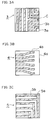
- Figs. 3A to 3C are plan views respectively showing the transferring metal band supplying members used in the present embodiment.
- the transferring metal band supplying member 3 has a structure in which metal bands 3b mainly composed of Ag and formed by a thin film forming process are formed on a supporting member 3a composed of a synthetic resin film such as a polyethylene terephtalate film or a polypropylene film.
- a supporting member 3a composed of a synthetic resin film such as a polyethylene terephtalate film or a polypropylene film.
- the thin film forming process include vacuum evaporation, sputtering, electroplating, electroless plating and ion plating.
- the metal bands 3b correspond to metal bands transferred in the region A in Fig. 2.
- a metal band supplying member 4 has a structure in which metal bands 4b mainly composed of Ag are formed by the thin film forming process on a supporting member 4a constructed similarly to the supporting member 3a.
- the metal bands 4b are in a shape transferred in the region B in Fig. 2.
- a transferring metal band supplying member 5 has a structure in which metal bands 5b mainly composed of Ag are formed by the thin film forming process on a supporting member 5a similarly constructed.
- the metal bands 5b are in such a plane shape as to form a conductive pattern in a portion corresponding to the region E in Fig. 2.
- transferring metal band supplying members for transferring metal bands are respectively prepared in the remaining regions shown in Fig. 2 in the same manner.
- the metal bands 3b, 4b and 5b are so respectively constructed as to form a mere wiring pattern
- some of the remaining transferring metal band supplying members have a structure in which a resistance film is connected to the middle of a metal band so as to construct a resistor.
- a resistance element is connected as shown to a portion indicated by reference numeral 6 in Fig. 1.
- the resistance film is transferred simultaneously with the transfer of the metal band by connecting the resistance film to a middle portion of the metal band as described above, to form such a resistance element.
- the conductive pattern 2 shown in Fig. 2 must be divided into a plurality of metal bands so as to be formed in a state where the metal bands formed on the plurality of transferring metal band supplying members are collected.
- a part of each of the metal bands 3b to 5b formed on the respective transferring metal band supplying members 3 to 5 may be provided with a coil-shaped pattern, as indicated by, for example, an arrow C in Fig. 3A, so that the coil-shaped pattern can function as an inductor.
- a functional conductive pattern portion shall be included in an expression "conductive pattern" in the present invention.
- powder of alumina Al2O3 and powder of borosilicate glass are respectively weighed so that the weight ratio is 55 : 45, are dispersed along with an organic binder in a solvent and are thoroughly mixed, thereby to obtain a slurry.
- the slurry obtained is used, thereby to produce a ceramic - glass raw sheet having a uniform thickness (10 ⁇ m) on a synthetic resin film.
- the ceramic - glass raw sheet is irradiated by laser light, thereby to form a through hole in a predetermined portion of the ceramic - glass raw sheet.
- the through hole is filled with a silver paste obtained by thoroughly mixing the powder of silver and that of glass, to form a through hole electrode.
- the ceramic - glass raw sheet having the through hole electrode formed therein is previously notched to predetermined lengths, as shown in Fig. 4A.
- the ceramic - glass raw sheet is located between a base plate 7 provided with a frame 7a and a punch 8, as shown in Fig. 4B.
- the frame 7a is moved up and down relative to the base plate 7, and is positioned at a height equal to or less than the height of the uppermost surface of raw sheets already laminated in the case of pressing, as described later.
- the punch 8 is also moved up and down and has a suction hole 8b for fixing the ceramic - glass raw sheet.
- the suction hole 8b is connected to a suction source such as a vacuum pump (not shown).
- a ceramic - glass raw sheet 9 prepared in the above described manner is pressed on raw sheets 9a to 9c already laminated inside of the base plate 7 by applying pressure using the punch 8 in a state where it is supported by a synthetic resin film 10, as shown in Fig. 5A. Thereafter, the synthetic resin film 10 fixed to the punch 8 by suction from the suction hole 8b is stripped from a cut portion of the ceramic - glass raw sheet 9 by raising the punch 8, thereby to obtain a raw substrate in which the ceramic - glass raw sheets 9 and 9a to 9c are affixed to each other.
- the metal bands are then sequentially transferred from the region A to the region T shown in Fig. 2, using the plurality of transferring metal band supplying members 11 including the transferring metal band supplying members shown in Figs. 3A to 3C between the punch 8 and the base plate 7, as shown in Fig. 5B, thereby to form the conductive pattern 2 shown in Fig. 1 which is constituted by the metal bands.
- a new ceramic - glass raw sheet is located between the punch 8 and the base plate 7.
- the new ceramic - glass raw sheet is pressed on a portion where the conductive pattern 2 is formed by repeating the foregoing process, and a conductive pattern is similarly formed again by a transfer process.
- the foregoing process is repeated a predetermined number of times, thereby to obtain a laminated raw substrate having a plurality of predetermined conductive pattern layers laminated in the frame 7a.
- the laminated raw substrate obtained is taken out of a laminated raw stage, is produced in a rectangular plane shape 50 mm square, and is sintered at a temperature of 900° , a predetermined outer electrode to be connected to an inner conductive pattern is formed by plating on a sintered multilayer substrate obtained, thereby to obtain a ceramic multilayer substrate.
- the method according to the present invention is used so as to form the conductive pattern in the ceramic multilayer substrate, the present invention is also applicable to a case where a conductive pattern is formed on a single plate type circuit board.
Landscapes
- Engineering & Computer Science (AREA)
- Manufacturing & Machinery (AREA)
- Microelectronics & Electronic Packaging (AREA)
- Manufacturing Of Printed Wiring (AREA)
- Parts Printed On Printed Circuit Boards (AREA)
Applications Claiming Priority (3)
| Application Number | Priority Date | Filing Date | Title |
|---|---|---|---|
| JP138603/93 | 1993-06-10 | ||
| JP13860393A JP3252534B2 (ja) | 1993-06-10 | 1993-06-10 | 基板への導電パターン形成方法 |
| JP13860393 | 1993-06-10 |
Publications (3)
| Publication Number | Publication Date |
|---|---|
| EP0629110A2 true EP0629110A2 (de) | 1994-12-14 |
| EP0629110A3 EP0629110A3 (de) | 1996-04-24 |
| EP0629110B1 EP0629110B1 (de) | 2002-01-23 |
Family
ID=15225955
Family Applications (1)
| Application Number | Title | Priority Date | Filing Date |
|---|---|---|---|
| EP94108706A Expired - Lifetime EP0629110B1 (de) | 1993-06-10 | 1994-06-07 | Verfahren zur Bildung eines leitfähigen Musters auf einem Substrat |
Country Status (3)
| Country | Link |
|---|---|
| EP (1) | EP0629110B1 (de) |
| JP (1) | JP3252534B2 (de) |
| DE (1) | DE69429690T2 (de) |
Cited By (3)
| Publication number | Priority date | Publication date | Assignee | Title |
|---|---|---|---|---|
| GB2290664A (en) * | 1994-06-14 | 1996-01-03 | Murata Manufacturing Co | Manufacturing a multilayer ceramic electrical component |
| EP1154469A1 (de) * | 2000-02-09 | 2001-11-14 | Matsushita Electric Industrial Co., Ltd. | Transfermaterial, seine Herstellung und damit hergestelltes Verbindungssubstrat |
| US8961725B2 (en) | 2010-02-09 | 2015-02-24 | Nederlandse Organisatie Voor Toegepast-Natuurwetenschappelijk Onderzoek Tno | Component placement on flexible and/or stretchable substrates |
Family Cites Families (3)
| Publication number | Priority date | Publication date | Assignee | Title |
|---|---|---|---|---|
| JPH0754780B2 (ja) * | 1987-08-10 | 1995-06-07 | 株式会社村田製作所 | 積層セラミックコンデンサの製造方法 |
| JPH04122093A (ja) * | 1990-09-13 | 1992-04-22 | Fujitsu Ltd | ペーストの転写方法と転写治具 |
| JP2990621B2 (ja) * | 1990-11-05 | 1999-12-13 | 株式会社村田製作所 | 積層セラミック電子部品の製造方法 |
-
1993
- 1993-06-10 JP JP13860393A patent/JP3252534B2/ja not_active Expired - Fee Related
-
1994
- 1994-06-07 EP EP94108706A patent/EP0629110B1/de not_active Expired - Lifetime
- 1994-06-07 DE DE69429690T patent/DE69429690T2/de not_active Expired - Lifetime
Cited By (10)
| Publication number | Priority date | Publication date | Assignee | Title |
|---|---|---|---|---|
| GB2290664A (en) * | 1994-06-14 | 1996-01-03 | Murata Manufacturing Co | Manufacturing a multilayer ceramic electrical component |
| US5700338A (en) * | 1994-06-14 | 1997-12-23 | Murata Manufacturing Co., Ltd. | Method of manufacturing resistor integrated in sintered body and method of manufacturing multilayer ceramic electronic component |
| GB2290664B (en) * | 1994-06-14 | 1998-03-04 | Murata Manufacturing Co | Method of manufacturing resistor integrated in sintered body and method of manufacturing multilayer ceramic electronic component |
| EP1154469A1 (de) * | 2000-02-09 | 2001-11-14 | Matsushita Electric Industrial Co., Ltd. | Transfermaterial, seine Herstellung und damit hergestelltes Verbindungssubstrat |
| EP1267594A3 (de) * | 2000-02-09 | 2003-01-02 | Matsushita Electric Industrial Co., Ltd. | Transfermaterial, seine Herstellung und damit hergestelltes Verbindungssubstrat |
| US6871396B2 (en) | 2000-02-09 | 2005-03-29 | Matsushita Electric Industrial Co., Ltd. | Transfer material for wiring substrate |
| EP1482543A3 (de) * | 2000-02-09 | 2005-06-08 | Matsushita Electric Industrial Co., Ltd. | Transfermaterial, seine Herstellung und damit hergestelltes Verbindungssubstrat |
| US6936774B2 (en) | 2000-02-09 | 2005-08-30 | Matsushita Electric Industrial Co., Ltd. | Wiring substrate produced by transfer material method |
| US7888789B2 (en) | 2000-02-09 | 2011-02-15 | Panasonic Corporation | Transfer material used for producing a wiring substrate |
| US8961725B2 (en) | 2010-02-09 | 2015-02-24 | Nederlandse Organisatie Voor Toegepast-Natuurwetenschappelijk Onderzoek Tno | Component placement on flexible and/or stretchable substrates |
Also Published As
| Publication number | Publication date |
|---|---|
| DE69429690T2 (de) | 2002-10-17 |
| EP0629110A3 (de) | 1996-04-24 |
| EP0629110B1 (de) | 2002-01-23 |
| JPH06350225A (ja) | 1994-12-22 |
| DE69429690D1 (de) | 2002-03-14 |
| JP3252534B2 (ja) | 2002-02-04 |
Similar Documents
| Publication | Publication Date | Title |
|---|---|---|
| EP1235235B1 (de) | Elektronische Bauteile und Verfahren zu ihrer Herstellung | |
| US5197170A (en) | Method of producing an LC composite part and an LC network part | |
| US7081803B2 (en) | Inductance element, laminated electronic component, laminated electronic component module and method for producing these element, component and module | |
| US7158005B2 (en) | Embedded toroidal inductor | |
| US4806188A (en) | Method for fabricating multilayer circuits | |
| EP0201583B1 (de) | Verfahren zum herstellen von verbindungsplatten mit dimensionaler stabilität und gemäss diesem verfahren hergestellte anordnung | |
| US20040239469A1 (en) | Embedded 3D coil inductors in a low temperature, co-fired ceramic substrate | |
| EP0901316B1 (de) | Herstellung eines mehrschichtigen keramischen Substrats mit einem passiven Bauelement | |
| US7232496B2 (en) | Multilayer ceramic electronic part, circuit board and method for producing ceramic green sheet used for manufacturing those part and circuit board | |
| JP3066455B2 (ja) | 異質材部を有するセラミックグリーンシート並びにセラミック積層体部品の製造方法 | |
| EP0629110B1 (de) | Verfahren zur Bildung eines leitfähigen Musters auf einem Substrat | |
| US5318820A (en) | HTCC/LTCC use of multiple ceramic tapes in high rate production | |
| US6627021B2 (en) | Method of manufacturing laminated ceramic electronic component and method of manufacturing laminated inductor | |
| CA2176789C (en) | Wiring board for mounting electronic devices with high-density terminals and method for producing wiring board | |
| JP4577479B2 (ja) | 多層配線基板形成に用いられる異材質部を有するシート形成方法および異材質部を有するシート | |
| JPH1187918A (ja) | 多層セラミック基板およびその製造方法 | |
| JP3147085B2 (ja) | 高周波濾波器及びその製造方法 | |
| KR100916075B1 (ko) | 다층 세라믹기판 제조방법 | |
| JPH0878270A (ja) | 積層コンデンサ基板 | |
| JPH0722752A (ja) | 多層セラミック基板およびその製造方法 | |
| JPH11224825A (ja) | 電子部品の製造方法 | |
| JPH06334304A (ja) | 基板への配線方法 | |
| JPH04364013A (ja) | 積層セラミックインダクタの製造法 | |
| JP2002185212A (ja) | 積層型共振器デバイス | |
| JP2004247679A (ja) | 電子部品の構成に用いられるシート |
Legal Events
| Date | Code | Title | Description |
|---|---|---|---|
| PUAI | Public reference made under article 153(3) epc to a published international application that has entered the european phase |
Free format text: ORIGINAL CODE: 0009012 |
|
| AK | Designated contracting states |
Kind code of ref document: A2 Designated state(s): DE FR GB |
|
| 17P | Request for examination filed |
Effective date: 19950223 |
|
| PUAL | Search report despatched |
Free format text: ORIGINAL CODE: 0009013 |
|
| AK | Designated contracting states |
Kind code of ref document: A3 Designated state(s): DE FR GB |
|
| GRAG | Despatch of communication of intention to grant |
Free format text: ORIGINAL CODE: EPIDOS AGRA |
|
| 17Q | First examination report despatched |
Effective date: 20010503 |
|
| GRAG | Despatch of communication of intention to grant |
Free format text: ORIGINAL CODE: EPIDOS AGRA |
|
| GRAH | Despatch of communication of intention to grant a patent |
Free format text: ORIGINAL CODE: EPIDOS IGRA |
|
| GRAH | Despatch of communication of intention to grant a patent |
Free format text: ORIGINAL CODE: EPIDOS IGRA |
|
| GRAA | (expected) grant |
Free format text: ORIGINAL CODE: 0009210 |
|
| REG | Reference to a national code |
Ref country code: GB Ref legal event code: IF02 |
|
| AK | Designated contracting states |
Kind code of ref document: B1 Designated state(s): DE FR GB |
|
| REF | Corresponds to: |
Ref document number: 69429690 Country of ref document: DE Date of ref document: 20020314 |
|
| ET | Fr: translation filed | ||
| PLBE | No opposition filed within time limit |
Free format text: ORIGINAL CODE: 0009261 |
|
| STAA | Information on the status of an ep patent application or granted ep patent |
Free format text: STATUS: NO OPPOSITION FILED WITHIN TIME LIMIT |
|
| 26N | No opposition filed | ||
| PGFP | Annual fee paid to national office [announced via postgrant information from national office to epo] |
Ref country code: FR Payment date: 20100709 Year of fee payment: 17 |
|
| PGFP | Annual fee paid to national office [announced via postgrant information from national office to epo] |
Ref country code: GB Payment date: 20100602 Year of fee payment: 17 Ref country code: DE Payment date: 20100602 Year of fee payment: 17 |
|
| GBPC | Gb: european patent ceased through non-payment of renewal fee |
Effective date: 20110607 |
|
| REG | Reference to a national code |
Ref country code: FR Ref legal event code: ST Effective date: 20120229 |
|
| REG | Reference to a national code |
Ref country code: DE Ref legal event code: R119 Ref document number: 69429690 Country of ref document: DE Effective date: 20120103 |
|
| PG25 | Lapsed in a contracting state [announced via postgrant information from national office to epo] |
Ref country code: FR Free format text: LAPSE BECAUSE OF NON-PAYMENT OF DUE FEES Effective date: 20110630 Ref country code: DE Free format text: LAPSE BECAUSE OF NON-PAYMENT OF DUE FEES Effective date: 20120103 |
|
| PG25 | Lapsed in a contracting state [announced via postgrant information from national office to epo] |
Ref country code: GB Free format text: LAPSE BECAUSE OF NON-PAYMENT OF DUE FEES Effective date: 20110607 |