EP0630061A1 - Verfahren zum Herstellen eines supraleitenden umkleideten Hochtemperaturdrahts - Google Patents
Verfahren zum Herstellen eines supraleitenden umkleideten Hochtemperaturdrahts Download PDFInfo
- Publication number
- EP0630061A1 EP0630061A1 EP94401297A EP94401297A EP0630061A1 EP 0630061 A1 EP0630061 A1 EP 0630061A1 EP 94401297 A EP94401297 A EP 94401297A EP 94401297 A EP94401297 A EP 94401297A EP 0630061 A1 EP0630061 A1 EP 0630061A1
- Authority
- EP
- European Patent Office
- Prior art keywords
- tube
- powder
- per hour
- hours
- equal
- Prior art date
- Legal status (The legal status is an assumption and is not a legal conclusion. Google has not performed a legal analysis and makes no representation as to the accuracy of the status listed.)
- Granted
Links
- 238000004519 manufacturing process Methods 0.000 title claims abstract description 9
- BQCADISMDOOEFD-UHFFFAOYSA-N Silver Chemical compound [Ag] BQCADISMDOOEFD-UHFFFAOYSA-N 0.000 claims abstract description 38
- 239000000843 powder Substances 0.000 claims abstract description 38
- 229910052709 silver Inorganic materials 0.000 claims abstract description 30
- 239000004332 silver Substances 0.000 claims abstract description 30
- 238000000034 method Methods 0.000 claims abstract description 24
- 239000000463 material Substances 0.000 claims abstract description 10
- 238000010438 heat treatment Methods 0.000 claims abstract description 9
- 239000012071 phase Substances 0.000 claims description 22
- 230000008569 process Effects 0.000 claims description 13
- IJGRMHOSHXDMSA-UHFFFAOYSA-N Atomic nitrogen Chemical compound N#N IJGRMHOSHXDMSA-UHFFFAOYSA-N 0.000 claims description 7
- MYMOFIZGZYHOMD-UHFFFAOYSA-N Dioxygen Chemical compound O=O MYMOFIZGZYHOMD-UHFFFAOYSA-N 0.000 claims description 7
- 239000002887 superconductor Substances 0.000 claims description 4
- 229910052757 nitrogen Inorganic materials 0.000 claims description 3
- 239000000969 carrier Substances 0.000 claims description 2
- 239000007791 liquid phase Substances 0.000 claims description 2
- 238000002844 melting Methods 0.000 claims description 2
- 230000008018 melting Effects 0.000 claims description 2
- 239000013081 microcrystal Substances 0.000 claims description 2
- 238000001556 precipitation Methods 0.000 claims description 2
- 230000003071 parasitic effect Effects 0.000 abstract description 6
- 230000007547 defect Effects 0.000 abstract description 2
- 238000000137 annealing Methods 0.000 description 5
- 230000009467 reduction Effects 0.000 description 5
- 229910052797 bismuth Inorganic materials 0.000 description 4
- 230000006835 compression Effects 0.000 description 4
- 238000007906 compression Methods 0.000 description 4
- 229910052745 lead Inorganic materials 0.000 description 4
- 230000006872 improvement Effects 0.000 description 3
- 239000000919 ceramic Substances 0.000 description 2
- 150000001875 compounds Chemical class 0.000 description 2
- 238000005096 rolling process Methods 0.000 description 2
- 101100296543 Caenorhabditis elegans pbo-4 gene Proteins 0.000 description 1
- 238000005054 agglomeration Methods 0.000 description 1
- 230000002776 aggregation Effects 0.000 description 1
- 230000009286 beneficial effect Effects 0.000 description 1
- 230000015572 biosynthetic process Effects 0.000 description 1
- 230000015556 catabolic process Effects 0.000 description 1
- 230000008859 change Effects 0.000 description 1
- 239000013065 commercial product Substances 0.000 description 1
- 238000002425 crystallisation Methods 0.000 description 1
- 230000008025 crystallization Effects 0.000 description 1
- 238000006731 degradation reaction Methods 0.000 description 1
- 238000011049 filling Methods 0.000 description 1
- 239000012467 final product Substances 0.000 description 1
- 239000010419 fine particle Substances 0.000 description 1
- 239000007788 liquid Substances 0.000 description 1
- 244000045947 parasite Species 0.000 description 1
- 239000002245 particle Substances 0.000 description 1
- 238000003825 pressing Methods 0.000 description 1
- 230000037452 priming Effects 0.000 description 1
- 239000000047 product Substances 0.000 description 1
- 238000003786 synthesis reaction Methods 0.000 description 1
- 230000009466 transformation Effects 0.000 description 1
Images

Classifications
-
- H—ELECTRICITY
- H10—SEMICONDUCTOR DEVICES; ELECTRIC SOLID-STATE DEVICES NOT OTHERWISE PROVIDED FOR
- H10N—ELECTRIC SOLID-STATE DEVICES NOT OTHERWISE PROVIDED FOR
- H10N60/00—Superconducting devices
- H10N60/01—Manufacture or treatment
- H10N60/0268—Manufacture or treatment of devices comprising copper oxide
- H10N60/0801—Manufacture or treatment of filaments or composite wires
Definitions
- the present invention relates to a process for manufacturing a wire sheathed in a superconductor at high critical temperature, and in particular the so-called “powder in tube” process described in particular in French patent FR-A-2 675 620.
- the multi-strand takes the form of a ribbon and the superconductive filaments acquire a very flat elliptical section; but the overall geometry is then very disordered; crossings of filaments occur which can cause breaks in continuity.
- Variant b) is described in US-A-5,114,908 and in the article published in "Cryogenics” 1992 52 (11) p. 940-947.
- the ratio of the useful cross-section of the wire to the total cross-section is less than 10% because of the large share taken up by the silver core.
- Variant c) is described in French patent FR-A-2,675,620.
- Stage 0 of this variant is distinct from that of variants a) and b) since it is rectangular.
- the billet is produced by stacking rectangular single strands in a square section tube; after closing under vacuum, this billet is stretched in a roller die until a ribbon of thickness less than 2 mm is obtained, itself laminated to 0.5 and even 0.3 mm.
- the filaments In the final state, the filaments have a thickness less than 20 microns and a form factor greater than 60.
- the superconductive material is generally introduced in the form of powder into the silver tube. But it was described in the article published in "App.Superconductivity" 1993-1- (10-12) p.1515-22 that one could introduce into the tube a cylindrical bar obtained by agglomeration of the powder by compression isostatic.
- the creepability of the ceramic depends on its particle size (elementary grain and size of the agglomerates) and on its crystallization state (grain morphology). These parameters change, in addition, during the transformation.
- the silver after annealing is much more ductile than the agglomerated powder, but it gradually hardens, hence problems of deformation due to the differences in creep of the two materials at a given time.
- a fine particle size ⁇ 30 microns causes the necking phenomenon leading to repeated breaks.
- the present invention aims to improve the "powder in tube” process so as, on the one hand to overcome the problems posed by the parasitic phases of the superconductive material, and on the other hand to improve the behavior of the wire during all the stretching phases.
- the duration of plateau at temperature T1 depends on the degree of synthesis of the powder used. It will be 45 to 60 hours for a 90% pure product and around 100 hours for a commercial product whose content in superconductive phase is generally less than 80%.
- the characteristic of the invention makes it possible, quite unexpectedly, to split the parasitic grains of said powder into smaller grains, and even to completely absorb them.
- the ceramic having recrystallized in the form of sheets, achieves a creep behavior in accordance with the ductility of silver.
- the flows are more regular and the efforts weaker; there are no more "jams" or priming strictions; the silver is less hardened and the creep of the two materials takes place harmoniously, keeping the ratio of the superconductive section to the total section constant, throughout the mechanical operations.
- Cylinders with a diameter of 10 mm are produced by isostatic compression of Bi2223 powder: (Bi, Pb) 2 Sr2 Ca2 Cu3 O10).
- These cylinders are introduced into a silver tube with an internal diameter of 10 mm and an external diameter of 12 mm; this tube is closed under vacuum.
- This billet is stretched in a circular die up to a diameter of 5 mm, then in a roller die until a ribbon of section 3x0.75 mm2 is obtained by applying, in both cases to each pass, a reduction coefficient of 10% in section (5% in diameter).
- a stress-relieving annealing of the silver sheath is carried out for 24 hours at 350 ° C., each time the cross-section has been reduced by 40%.
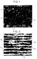
- Figure 1 shows a section of single strand obtained.
- the structure is heterogeneous.
- the grains 1 of phase Bi2223 which appear gray are rounded and those of parasitic phases 3.2 which appear white and black are large and poorly distributed.
- the single-strand is cut into sections which are inserted, in bundles of fifteen sections, in a square section tube with an inside side of 10 mm and an outside side of 12 mm; this tube is closed under vacuum.
- the billet thus formed is stretched in a roller die.
- the ribbon is brought to its final dimension of 3 ⁇ 0.5 mm2 and heat treated for 60 hours at 815 ° C. in an oxygenated atmosphere.
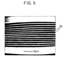
- the final strand has a regular geometry made up of filaments 15 to 20 microns thick, having a form factor greater than 60, but there is a degradation of the geometry by hard phase nodules parasites of the superconductive material having deformed the silver walls.
- Figure 2 in section the filaments 10 and their silver sheath 11, and hard nodules referenced 12 (Ca2 Cu03) and 13 (Ca2 PbO4).
- FIG. 3 we see the location 14 of an old nodule 12 or 13 which has been retransformed into the superconductive phase Bi2223 during the final heat treatment which is subjected to the wire; a cavity remains at location 14 of the old nodule 12 or 13.
- Cylinders with a diameter of 10 mm are produced by isostatic compression of stoichiometric Bi2223 powder as in Example 1.
- the bars do not shrink. They are then introduced into a silver tube with an internal diameter of 10 mm and an external diameter of 12 mm; this tube is closed under vacuum.
- This billet is stretched in a circular die up to a diameter of 5 mm, then in a roller die until a ribbon with a section of 2.4 ⁇ 0.75 mm2 is obtained by applying, in both cases to each pass, a reduction coefficient of 15% in section (8% in diameter). Only one stress relieving of the silver sheath is carried out for 24 hours at 350 ° C.
- the single strand obtained is visible in section in FIG. 4. If we compare to the section in FIG. 1, we see that the grains of parasitic phases 5 are smaller or cleaved and that they are better distributed in a homogeneous structure 6 of phase Bi2223 recrystallized from sheets.
- the single strand is cut into sections which are inserted, in four packs of thirteen sections, into a tube with a square section with an inside side of 10 mm and an outside side of 12 mm; this tube is closed under vacuum.
- the billet thus formed is stretched into a roller die and the ribbon is brought to its final dimension of 3 ⁇ 0.5 mm2 and thermally reprocessed as in Example 1.
- the multifilament strand thus obtained is visible in section in FIG. 5; it has a regular and flawless geometry made up of filaments 30 of thickness 15 to 20 microns, having a form factor greater than 60.
- Example 2 It is identical to Example 2 according to the invention, except for the powder used which is a non-stoichiometric powder of formula (Bi, Pb) 2 Sr 1.6 Ca2 Cu 2.8 O 9.2 .
- T1 800 ° C for 100 hours.
- T2 700 ° C with a descent speed between T1 and T2 equal to 3 ° C per hour.
- T3 450 ° C with a descent between T2 and T3 equal to 200 ° C per hour. Stop at T3 under pure oxygen for 20 hours.
- Example 2 It is identical to Example 2 according to the invention except as regards the powder used which has the formula Bi2 Sr2 Ca Cu2 O8 and an initial temperature rise equal to 870 ° C.
- T2 820 ° C with a lowering speed between T1 and T2 equal at 3 ° C per hour.
- T3 650 ° C with a descent speed between T2 and T3 equal to 200 ° C per hour. Stop at T3 under pure nitrogen for 40 hours.
- Cylinders with a diameter of 7 mm are produced by isostatic compression of YBa2 Cu3 O7 powder.
- the bars having withdrawn, their diameter increased to 6 mm. They are then introduced into a silver tube with an internal diameter of 6 mm and an external diameter of 8 mm; this tube is closed under vacuum.
- This billet is drawn in a circular die up to a diameter of 3 mm, then in a roller die until a ribbon of section 2.4 ⁇ 0.75 mm2 is obtained by applying, in both cases to each operation, a reduction coefficient of 10% in section (5% in diameter). Only one stress relief annealing of the silver sheath is carried out for 24 hours at 350 ° C. before the drawing is started in the roller die.
- the wire thus obtained is cut into sections which are inserted, in four bundles of thirteen sections, in a tube with a square section with an inside side of 10 mm and an outside side of 12 mm; this tube is closed under vacuum.
- the billet thus formed is stretched in a roller die to its final dimension of 3x0.5 mm2 and thermally reprocessed.
- the final strand has a regular geometry made up of filaments 15 to 20 microns thick, having a form factor greater than 60.
Landscapes
- Engineering & Computer Science (AREA)
- Manufacturing & Machinery (AREA)
- Superconductors And Manufacturing Methods Therefor (AREA)
- Inorganic Compounds Of Heavy Metals (AREA)
- Eyeglasses (AREA)
Applications Claiming Priority (2)
| Application Number | Priority Date | Filing Date | Title |
|---|---|---|---|
| FR9306993 | 1993-06-10 | ||
| FR9306993A FR2706673B1 (fr) | 1993-06-10 | 1993-06-10 | Procédé de fabrication d'un fil gainé en supraconducteur à haute température critique. |
Publications (2)
| Publication Number | Publication Date |
|---|---|
| EP0630061A1 true EP0630061A1 (de) | 1994-12-21 |
| EP0630061B1 EP0630061B1 (de) | 1996-09-25 |
Family
ID=9447979
Family Applications (1)
| Application Number | Title | Priority Date | Filing Date |
|---|---|---|---|
| EP94401297A Expired - Lifetime EP0630061B1 (de) | 1993-06-10 | 1994-06-09 | Verfahren zum Herstellen eines supraleitenden umkleideten Hochtemperaturdrahts |
Country Status (8)
| Country | Link |
|---|---|
| US (1) | US5594932A (de) |
| EP (1) | EP0630061B1 (de) |
| JP (1) | JPH08500466A (de) |
| CA (1) | CA2125446C (de) |
| DE (1) | DE69400600T2 (de) |
| ES (1) | ES2092870T3 (de) |
| FR (1) | FR2706673B1 (de) |
| WO (1) | WO1994029905A1 (de) |
Cited By (1)
| Publication number | Priority date | Publication date | Assignee | Title |
|---|---|---|---|---|
| EP1070327A4 (de) * | 1998-03-18 | 2007-05-09 | S C Power Systems Inc | Integriertes band |
Families Citing this family (5)
| Publication number | Priority date | Publication date | Assignee | Title |
|---|---|---|---|---|
| DE19722779A1 (de) | 1997-06-02 | 1998-12-03 | Hoechst Ag | Formkörper aus texturiertem Supraleitermaterial und Verfahren zu ihrer Herstellung |
| DE19906298A1 (de) * | 1998-03-06 | 1999-09-09 | Siemens Ag | Bandförmiger Multifilamentsupraleiter mit Bi-Cuprat-Filamenten |
| US7749557B2 (en) * | 2004-06-22 | 2010-07-06 | Sumitomo Electric Industries, Ltd. | Method of manufacturing superconducting wire |
| JP4715672B2 (ja) * | 2006-08-04 | 2011-07-06 | 住友電気工業株式会社 | 酸化物超電導線材およびその製造方法 |
| CN108257729B (zh) * | 2017-12-13 | 2024-07-05 | 无锡友方电工股份有限公司 | 磁共振磁体mri月牙形超导基体、超导线及制造方法 |
Citations (4)
| Publication number | Priority date | Publication date | Assignee | Title |
|---|---|---|---|---|
| WO1989006053A1 (fr) * | 1987-12-15 | 1989-06-29 | Siemens Aktiengesellschaft | Procede de fabrication de fils metalliques ou de bandes en materiaux supraconducteurs a temperature elevee et gaines utilisees pour appliquer le procede |
| EP0404966A1 (de) * | 1989-01-14 | 1991-01-02 | Sumitomo Electric Industries, Ltd. | Verfahren zur herstellung eines supraleitfähigen drahts vom keramischen typ |
| EP0457929A1 (de) * | 1990-04-27 | 1991-11-27 | Siemens Aktiengesellschaft | Verfahren zum Herstellen eines hochtemperatur-supraleitenden Bauteiles und hochtemperatur-supraleitendes Bauteil |
| EP0559574A1 (de) * | 1992-03-06 | 1993-09-08 | Alcatel | Verfahren zur Herstellung eines Yttrium-Barium-Kupfer-Oxid-Pulvers (123 Typ) zur Formgebung durch Streckung-Laminierung |
Family Cites Families (5)
| Publication number | Priority date | Publication date | Assignee | Title |
|---|---|---|---|---|
| DE3887910T2 (de) * | 1987-03-20 | 1994-08-04 | Fujikura Ltd., Tokio/Tokyo | Verfahren zur Herstellung eines Drahtes aus supraleitendem Oxid und damit hergestellter Draht. |
| JPS6465716A (en) * | 1987-09-04 | 1989-03-13 | Furukawa Electric Co Ltd | Manufacture of oxide superconductive wire |
| JPH0473821A (ja) * | 1990-07-16 | 1992-03-09 | Sumitomo Electric Ind Ltd | 酸化物超電導線材の製造方法 |
| US5189260A (en) * | 1991-02-06 | 1993-02-23 | Iowa State University Research Foundation, Inc. | Strain tolerant microfilamentary superconducting wire |
| US5395821A (en) * | 1992-10-30 | 1995-03-07 | Martin Marietta Energy Systems, Inc. | Method of producing Pb-stabilized superconductor precursors and method of producing superconductor articles therefrom |
-
1993
- 1993-06-10 FR FR9306993A patent/FR2706673B1/fr not_active Expired - Fee Related
-
1994
- 1994-06-08 CA CA002125446A patent/CA2125446C/fr not_active Expired - Fee Related
- 1994-06-09 JP JP7501418A patent/JPH08500466A/ja active Pending
- 1994-06-09 ES ES94401297T patent/ES2092870T3/es not_active Expired - Lifetime
- 1994-06-09 DE DE69400600T patent/DE69400600T2/de not_active Expired - Fee Related
- 1994-06-09 WO PCT/FR1994/000685 patent/WO1994029905A1/fr not_active Ceased
- 1994-06-09 EP EP94401297A patent/EP0630061B1/de not_active Expired - Lifetime
- 1994-06-09 US US08/257,304 patent/US5594932A/en not_active Expired - Fee Related
Patent Citations (4)
| Publication number | Priority date | Publication date | Assignee | Title |
|---|---|---|---|---|
| WO1989006053A1 (fr) * | 1987-12-15 | 1989-06-29 | Siemens Aktiengesellschaft | Procede de fabrication de fils metalliques ou de bandes en materiaux supraconducteurs a temperature elevee et gaines utilisees pour appliquer le procede |
| EP0404966A1 (de) * | 1989-01-14 | 1991-01-02 | Sumitomo Electric Industries, Ltd. | Verfahren zur herstellung eines supraleitfähigen drahts vom keramischen typ |
| EP0457929A1 (de) * | 1990-04-27 | 1991-11-27 | Siemens Aktiengesellschaft | Verfahren zum Herstellen eines hochtemperatur-supraleitenden Bauteiles und hochtemperatur-supraleitendes Bauteil |
| EP0559574A1 (de) * | 1992-03-06 | 1993-09-08 | Alcatel | Verfahren zur Herstellung eines Yttrium-Barium-Kupfer-Oxid-Pulvers (123 Typ) zur Formgebung durch Streckung-Laminierung |
Cited By (1)
| Publication number | Priority date | Publication date | Assignee | Title |
|---|---|---|---|---|
| EP1070327A4 (de) * | 1998-03-18 | 2007-05-09 | S C Power Systems Inc | Integriertes band |
Also Published As
| Publication number | Publication date |
|---|---|
| FR2706673A1 (fr) | 1994-12-23 |
| WO1994029905A1 (fr) | 1994-12-22 |
| FR2706673B1 (fr) | 1995-08-18 |
| US5594932A (en) | 1997-01-14 |
| EP0630061B1 (de) | 1996-09-25 |
| CA2125446C (fr) | 2000-02-15 |
| ES2092870T3 (es) | 1996-12-01 |
| DE69400600D1 (de) | 1996-10-31 |
| JPH08500466A (ja) | 1996-01-16 |
| CA2125446A1 (fr) | 1994-12-11 |
| DE69400600T2 (de) | 1997-02-06 |
Similar Documents
| Publication | Publication Date | Title |
|---|---|---|
| EP0630061B1 (de) | Verfahren zum Herstellen eines supraleitenden umkleideten Hochtemperaturdrahts | |
| FR2680598A1 (fr) | Procede de fabrication d'un fil supraconducteur. | |
| EP0540416B1 (de) | Verfahren zur Herstellung eines flexiblen Hochtemperatur-Supraleiters und resultierender Leiter | |
| EP0318921B1 (de) | Supraleitender, gemischter Draht mit hoher Springtemperatur und Verfahren zu dessen Herstellung | |
| EP0867950B1 (de) | Verfahren zur Entkopplung eines HTc multifilamentären Draht mit silberner Matrix und so hergestellter multifilamentärer Draht | |
| EP0509436B1 (de) | Verfahren zum Herstellen von oxyd-supraleitenden multifilamentären Drähten und Drähte, erzeugt mit diesem Verfahren | |
| FR2539550A1 (fr) | Procede de fabrication de supraconducteurs stabilises par de l'aluminium, et supraconducteur ainsi produit | |
| EP0390016B1 (de) | Herstellungsverfahren eines supraleitenden oxydischen Bands | |
| EP0474566B1 (de) | Verfahren zur Kristallisierung in Gegenwart eines magnetischen Feldes | |
| EP1160224B1 (de) | Verfahren zur Herstellung von Zirkonoxid-Körper mit einem metallisch-goldenen Aussehen | |
| EP1252662B1 (de) | Supraleiter mit kryogenem stabilisator auf aluminiumbasis | |
| EP1050911A1 (de) | Hochtemperatur supraleitender Draht, Verfahren dessen Herstellung | |
| CA2030483C (fr) | Methode de fabrication acceleree de fils ou rubans de ceramique supraconductrice | |
| EP0531188B1 (de) | Verfahren zur Herstellung eines Verbundleiters aus Metall und Hoch-Temperatur-Supraleiter | |
| EP0357480B1 (de) | Zusammengesetzte Elemente mit einem Herzstück aus supraleitendem Material und Verfahren zu ihrer Herstellung | |
| FR2690271A1 (fr) | Procédé de réalisation d'un conducteur composite métal-supraconducteur à haute température critique. | |
| EP0559574B1 (de) | Verfahren zur Herstellung eines Yttrium-Barium-Kupfer-Oxid-Pulvers (123 Typ) zur Formgebung durch Streckung-Laminierung | |
| EP0886327A1 (de) | Verfahren zur Texturierung eines supraleitenden HTC Leiter und nach diesen Verfahren hergestellte Leiter | |
| FR2783084A1 (fr) | Supraconducteur a plusieurs ames en courant alternatif a haut point critique et son procede de fabrication | |
| FR2752327A1 (fr) | Brin htc multifilamentaire a disposition interne decalee | |
| FR2767538A1 (fr) | Procede de fabrication d'une bande en alliage du type fer-nickel a partir d'un demi produit de coulee continue | |
| FR2787785A1 (fr) | Procede de preparation d'un supraconducteur oxyde ayant une grande partie de la phase bismuth du type 2223 et utilisation du procede | |
| EP1613786A1 (de) | Herstellungsprozess eines werkstückes aus silberlegierung und legierung für diesen prozess | |
| FR2787622A1 (fr) | Procede de fabrication d'un ruban supraconducteur a haute tc, et dispositif pour sa mise en oeuvre | |
| BE693330A (de) |
Legal Events
| Date | Code | Title | Description |
|---|---|---|---|
| PUAI | Public reference made under article 153(3) epc to a published international application that has entered the european phase |
Free format text: ORIGINAL CODE: 0009012 |
|
| AK | Designated contracting states |
Kind code of ref document: A1 Designated state(s): CH DE ES FR GB IT LI NL SE |
|
| 17P | Request for examination filed |
Effective date: 19950515 |
|
| GRAG | Despatch of communication of intention to grant |
Free format text: ORIGINAL CODE: EPIDOS AGRA |
|
| GRAH | Despatch of communication of intention to grant a patent |
Free format text: ORIGINAL CODE: EPIDOS IGRA |
|
| 17Q | First examination report despatched |
Effective date: 19960306 |
|
| GRAH | Despatch of communication of intention to grant a patent |
Free format text: ORIGINAL CODE: EPIDOS IGRA |
|
| GRAA | (expected) grant |
Free format text: ORIGINAL CODE: 0009210 |
|
| AK | Designated contracting states |
Kind code of ref document: B1 Designated state(s): CH DE ES FR GB IT LI NL SE |
|
| REG | Reference to a national code |
Ref country code: CH Ref legal event code: NV Representative=s name: GEC ALSTHOM (SUISSE) S.A. DEPARTEMENT DES BREVETS |
|
| ITF | It: translation for a ep patent filed | ||
| GBT | Gb: translation of ep patent filed (gb section 77(6)(a)/1977) |
Effective date: 19961007 |
|
| REF | Corresponds to: |
Ref document number: 69400600 Country of ref document: DE Date of ref document: 19961031 |
|
| REG | Reference to a national code |
Ref country code: ES Ref legal event code: FG2A Ref document number: 2092870 Country of ref document: ES Kind code of ref document: T3 |
|
| PLBE | No opposition filed within time limit |
Free format text: ORIGINAL CODE: 0009261 |
|
| STAA | Information on the status of an ep patent application or granted ep patent |
Free format text: STATUS: NO OPPOSITION FILED WITHIN TIME LIMIT |
|
| 26N | No opposition filed | ||
| PGFP | Annual fee paid to national office [announced via postgrant information from national office to epo] |
Ref country code: GB Payment date: 19990511 Year of fee payment: 6 |
|
| PGFP | Annual fee paid to national office [announced via postgrant information from national office to epo] |
Ref country code: FR Payment date: 19990512 Year of fee payment: 6 |
|
| PGFP | Annual fee paid to national office [announced via postgrant information from national office to epo] |
Ref country code: CH Payment date: 19990514 Year of fee payment: 6 |
|
| PGFP | Annual fee paid to national office [announced via postgrant information from national office to epo] |
Ref country code: SE Payment date: 19990525 Year of fee payment: 6 Ref country code: DE Payment date: 19990525 Year of fee payment: 6 |
|
| PGFP | Annual fee paid to national office [announced via postgrant information from national office to epo] |
Ref country code: NL Payment date: 19990527 Year of fee payment: 6 |
|
| PGFP | Annual fee paid to national office [announced via postgrant information from national office to epo] |
Ref country code: ES Payment date: 19990621 Year of fee payment: 6 |
|
| REG | Reference to a national code |
Ref country code: FR Ref legal event code: CD |
|
| PG25 | Lapsed in a contracting state [announced via postgrant information from national office to epo] |
Ref country code: GB Free format text: LAPSE BECAUSE OF NON-PAYMENT OF DUE FEES Effective date: 20000609 |
|
| PG25 | Lapsed in a contracting state [announced via postgrant information from national office to epo] |
Ref country code: SE Free format text: LAPSE BECAUSE OF NON-PAYMENT OF DUE FEES Effective date: 20000610 Ref country code: ES Free format text: THE PATENT HAS BEEN ANNULLED BY A DECISION OF A NATIONAL AUTHORITY Effective date: 20000610 |
|
| PG25 | Lapsed in a contracting state [announced via postgrant information from national office to epo] |
Ref country code: LI Free format text: LAPSE BECAUSE OF NON-PAYMENT OF DUE FEES Effective date: 20000630 Ref country code: CH Free format text: LAPSE BECAUSE OF NON-PAYMENT OF DUE FEES Effective date: 20000630 |
|
| PG25 | Lapsed in a contracting state [announced via postgrant information from national office to epo] |
Ref country code: NL Free format text: LAPSE BECAUSE OF NON-PAYMENT OF DUE FEES Effective date: 20010101 |
|
| GBPC | Gb: european patent ceased through non-payment of renewal fee |
Effective date: 20000609 |
|
| REG | Reference to a national code |
Ref country code: CH Ref legal event code: PL |
|
| EUG | Se: european patent has lapsed |
Ref document number: 94401297.0 |
|
| PG25 | Lapsed in a contracting state [announced via postgrant information from national office to epo] |
Ref country code: FR Free format text: LAPSE BECAUSE OF NON-PAYMENT OF DUE FEES Effective date: 20010228 |
|
| NLV4 | Nl: lapsed or anulled due to non-payment of the annual fee |
Effective date: 20010101 |
|
| REG | Reference to a national code |
Ref country code: FR Ref legal event code: ST |
|
| PG25 | Lapsed in a contracting state [announced via postgrant information from national office to epo] |
Ref country code: DE Free format text: LAPSE BECAUSE OF NON-PAYMENT OF DUE FEES Effective date: 20010403 |
|
| REG | Reference to a national code |
Ref country code: ES Ref legal event code: FD2A Effective date: 20020304 |
|
| PG25 | Lapsed in a contracting state [announced via postgrant information from national office to epo] |
Ref country code: IT Free format text: LAPSE BECAUSE OF NON-PAYMENT OF DUE FEES;WARNING: LAPSES OF ITALIAN PATENTS WITH EFFECTIVE DATE BEFORE 2007 MAY HAVE OCCURRED AT ANY TIME BEFORE 2007. THE CORRECT EFFECTIVE DATE MAY BE DIFFERENT FROM THE ONE RECORDED. Effective date: 20050609 |