EP0630108A2 - Procédé pour l'extension de la gamme de fréquences d'un signal audio numérique - Google Patents
Procédé pour l'extension de la gamme de fréquences d'un signal audio numérique Download PDFInfo
- Publication number
- EP0630108A2 EP0630108A2 EP94304002A EP94304002A EP0630108A2 EP 0630108 A2 EP0630108 A2 EP 0630108A2 EP 94304002 A EP94304002 A EP 94304002A EP 94304002 A EP94304002 A EP 94304002A EP 0630108 A2 EP0630108 A2 EP 0630108A2
- Authority
- EP
- European Patent Office
- Prior art keywords
- digital audio
- audio signal
- frequency range
- frequency
- digital
- Prior art date
- Legal status (The legal status is an assumption and is not a legal conclusion. Google has not performed a legal analysis and makes no representation as to the accuracy of the status listed.)
- Granted
Links
Images
Classifications
-
- H—ELECTRICITY
- H03—ELECTRONIC CIRCUITRY
- H03H—IMPEDANCE NETWORKS, e.g. RESONANT CIRCUITS; RESONATORS
- H03H17/00—Networks using digital techniques
-
- G—PHYSICS
- G11—INFORMATION STORAGE
- G11B—INFORMATION STORAGE BASED ON RELATIVE MOVEMENT BETWEEN RECORD CARRIER AND TRANSDUCER
- G11B20/00—Signal processing not specific to the method of recording or reproducing; Circuits therefor
- G11B20/10—Digital recording or reproducing
- G11B20/10527—Audio or video recording; Data buffering arrangements
Definitions
- the present invention relates generally to improvements in audio signal processing, and more specifically to a method of expanding a frequency range of a digital audio signal without increasing a sampling rate which has been utilized for converting an original analog audio signal to the digital audio signal.
- an analog audio signal such as a speech signal is converted into a digital signal and then is stored, for later use, in an appropriate storage medium such a RAM (random access memory), a magnetic tape, etc.
- RAM random access memory
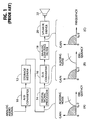
- Fig. 1 is a diagram schematically showing such a known technique.
- the arrangement of Fig. 1 includes a plurality of functional blocks together with three sketches each of which schematically illustrates spectrum distribution of a digital signal appearing at the functional blocks.
- an analog-to-digital (A/D) converter 10 is supplied with an analog signal such as a speech signal.
- the A/D converter 10 samples the incoming analog signal and then quantizes the sampled values as is well known in the art.
- a digital audio signal thus obtained is stored in a suitable storage medium 12 such as a RAM. Representing a sampling rate as f s , a sampling theorem tells us that the digital signal stored in the storage medium 12 has a frequency spectrum (frequency range) extending from 0Hz to f s /2.
- a digital audio signal retrieved from the storage medium 12 is applied to a digital signal processor 14.
- the spectrum of the digital signal is schematically shown in a sketch (A) of Fig. 1.
- the digital audio signal hatchched portion
- the digital audio signal has a frequency range from 0Hz to f s /2 and accompanying aliasing noises.
- the spectra of the digital signal and the noises are symmetrical with respect to the frequency f s /2.
- the digital signal processor 14 operates such as to shift the aliasing noises toward a higher frequency range. In other words, the processor 14 moves only the aliasing noises away from f s /2. Thereafter, the output of the digital signal processor 14 is applied to a digital-to-analog converter 16 wherein the digital signal is converted into the corresponding analog signal. Subsequently, an analog low-pass filter 18 allows the audio signal (hatched portion) to pass therethrough. Thus, the aliasing noises can be blocked at the low-pass filter 18.
- the reproduced analog signal is applied to a speaker 22 via a speaker driver 20 which includes an audio frequency amplifier as is known in the art.
- the digital audio signal has the frequency range from 0Hz to 4kHz. If it is desired to reproduce a sound at the speaker 22 in a more natural manner, the frequency range of the stored digital signal should be expanded up to a higher frequency (for example, about 8kHz). This implies that the sampling rate should be increased to 16kHz (8kHz ⁇ 2).
- the above object is achieved by techniques wherein a frequency range of a digital audio signal is effectively expanded without increasing a sampling frequency which has been used for generating the digital audio signal.
- the digital audio signal is divided into first and second digital audio signals.
- the first digital audio signal is delayed by a predetermined time duration in order to be combined, at a later time, with the second digital audio signal which is to be subject to digital processing.
- the second digital audio signal undergoes band-pass filtering.
- the frequency range of the second digital audio signal which has been band-pass filtered is expanded.
- the second digital audio signal whose frequency range has been expanded is combined with the first digital audio signal which has been delayed.
- the digital audio signal is expanded in terms of its frequency range.
- a first aspect of the present invention resides in a method of expanding a frequency range of a digital audio signal which has been sampled by a frequency f s , the digital audio signal having a frequency range whose upper frequency is defined by a frequency f s /2, the method comprising the steps of: (a) splitting the digital audio signal into first and second digital audio signals; (b) delaying the first digital audio signal by a predetermined time duration; (c) bandpass filtering the second digital audio signal, the second digital audio signal, after being subjected to the band-pass filtering, having a first frequency range defined by frequencies f1 and f2 (0 ⁇ f1 ⁇ f2 ⁇ f s ); (d) expanding the first frequency range of the second digital audio signal over a second frequency range; (e) combining the first and second digital audio signals for generating a third digital audio signal with an expanded frequency range.
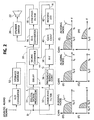
- FIG. 2 further illustrates six sketches (D)-(H) each showing spectrum distribution of digital signals appearing at the blocks of Fig. 2.
- the arrangement of the blocks of Fig. 2 differs from that of Fig. 1 in that the former arrangement further includes a frequency range expander 30 enclosed by a dashed line.
- Each of the blocks of the frequency range expander 30 is well known to one of ordinary skill in the art.
- the present invention resides in an improved method which can be achieved by combining such known functional blocks.
- a digital audio signal is stored in the storage medium 12 such as a RAM (random access memory), a magnetic tape, etc.
- the sampling rate f s at the A/D converter 10 is 8kHz merely by way of example.
- the digital audio signal D is retrieved from the storage medium 12 and then is applied to both the digital signal processor 14 and a band-pass filter 32 which forms part of the frequency range expander 30.
- the digital signal processor 14 operates such as to shift the aliasing noises toward a higher frequency range.
- the aliasing noise is shifted above the sampling frequency f s as illustrated in the sketch (E).
- the output of the processor 14 is applied to a delay circuit 34.
- the delay circuit 34 is to delay the digital audio signal D by a time duration which is required for processing a digital signal at blocks 32, 36, 38, 40, and 42.
- the band-pass filter 32 is to filter signal components between f s /4 and f s /2 of the digital signal D, as shown in the sketch (F).
- the output F of the band-pass filter 32 is then applied to a frequency range controller 36 wherein the frequency range from f s /4 to f s /2 is doubled in this particular case. Therefore, the output G of the frequency range controller 36 exhibits a frequency range shown in the sketch (G).
- the output G of the controller 36 is applied to a FFT (Fast Fourier Transformer) 38 wherein a time domain signal is changed to a frequency domain signal in order to be processed in the next stage, viz., a gain controller 40.
- FFT Fast Fourier Transformer
- the gain controller 40 operates such as to regulate the signal gain over the frequency range (from f s /2 to f s ) of the signal G in order to improve the sense of hearing when the reproduced analog signal drives the speaker 22.
- the response of a human ear to sound depends on the frequency of the sound as well as its intensity. The ear is more sensitive to some frequencies than to others. The ear is most sensitive near 4kHz. At frequencies other than this, the sound must be made more intense before it is audible.
- the gain controller 40 is to regulate the audio signal gains of the digital signal applied from the FFT to an appropriate levels.
- the output of the gain controller 40 is restored to a time domain signal using a reverse FFT 42.
- the spectrum of the output H of the reverse FFT 42 is schematically shown in the sketch H.
- a signal combiner 44 is supplied with the two outputs of the delay circuit 34 and the reverse FFT 42, and combines them as shown in the sketch (I).
- the delay circuit 34 is to retard the output E of the digital signal processor 14 by a time duration which is required for completing the signal processing at the reverse FFT 42.
- the output I of the signal combiner 44 has a frequency range extending from 0Hz to 8kHz (viz., the sampling rate f s ) in this particular case.
- the D/A converter 16 converts the digital output I into the corresponding analog signal.
- the low-pass filter 18 is designed such as to pass the analog signal components from 0Hz to 8kHz (viz., f s ) and to block the aliasing noises. Thus, a more natural sound can be obtained from the speaker 22 as compared with the prior art without increasing the sampling frequency f s .
- a goal of the present invention is to expand the frequency range of the output F of the filter 32 and then combine the delayed digital signal and the output H of the reverse FFT 42. Accordingly, it is understood that the present invention is in no way limited to the In the foregoing, the band-pass filter 32 passes the band-pass filtering of the digital signal to the frequency range from f s to f s /2. That is, such a band-pass filtering is merely exemplary.
Landscapes
- Engineering & Computer Science (AREA)
- Multimedia (AREA)
- Signal Processing (AREA)
- Analogue/Digital Conversion (AREA)
- Stereophonic System (AREA)
- Filters That Use Time-Delay Elements (AREA)
- Cable Transmission Systems, Equalization Of Radio And Reduction Of Echo (AREA)
Applications Claiming Priority (2)
| Application Number | Priority Date | Filing Date | Title |
|---|---|---|---|
| JP133067/93 | 1993-06-03 | ||
| JP5133067A JPH06350401A (ja) | 1993-06-03 | 1993-06-03 | ディジタルフィルタ |
Publications (3)
| Publication Number | Publication Date |
|---|---|
| EP0630108A2 true EP0630108A2 (fr) | 1994-12-21 |
| EP0630108A3 EP0630108A3 (fr) | 1996-01-17 |
| EP0630108B1 EP0630108B1 (fr) | 1998-10-28 |
Family
ID=15096070
Family Applications (1)
| Application Number | Title | Priority Date | Filing Date |
|---|---|---|---|
| EP19940304002 Expired - Lifetime EP0630108B1 (fr) | 1993-06-03 | 1994-06-03 | Procédé pour l'extension de la gamme de fréquences d'un signal audio numérique |
Country Status (3)
| Country | Link |
|---|---|
| EP (1) | EP0630108B1 (fr) |
| JP (1) | JPH06350401A (fr) |
| DE (1) | DE69414179T2 (fr) |
Cited By (2)
| Publication number | Priority date | Publication date | Assignee | Title |
|---|---|---|---|---|
| CN101556800B (zh) * | 2003-10-23 | 2012-05-23 | 松下电器产业株式会社 | 音频频谱编解码方法和装置、声音信号发送和接收装置 |
| US9241215B2 (en) | 2012-08-03 | 2016-01-19 | Samsung Electronics Co., Ltd | Mobile apparatus and control method thereof |
Families Citing this family (1)
| Publication number | Priority date | Publication date | Assignee | Title |
|---|---|---|---|---|
| NZ532572A (en) * | 2004-04-26 | 2006-10-27 | Phitek Systems Ltd | Audio signal processing for generating apparent bass through harmonics |
Family Cites Families (5)
| Publication number | Priority date | Publication date | Assignee | Title |
|---|---|---|---|---|
| JPS5754993A (en) * | 1980-09-18 | 1982-04-01 | Yoshihiko Akiba | Tone quality improving device |
| JPS6016200B2 (ja) * | 1982-02-23 | 1985-04-24 | 株式会社東芝 | ヒステリシス電動機の運転制御装置 |
| JPS62171300A (ja) * | 1986-01-23 | 1987-07-28 | Fujitsu Ten Ltd | 音響機器の騒音補償装置 |
| JPH04348686A (ja) * | 1991-05-27 | 1992-12-03 | Kobe Nippon Denki Software Kk | 光学式ビデオディスクの映像信号記録方式 |
| JPH0685607A (ja) * | 1992-08-31 | 1994-03-25 | Alpine Electron Inc | 高域成分復元装置 |
-
1993
- 1993-06-03 JP JP5133067A patent/JPH06350401A/ja active Pending
-
1994
- 1994-06-03 DE DE1994614179 patent/DE69414179T2/de not_active Expired - Lifetime
- 1994-06-03 EP EP19940304002 patent/EP0630108B1/fr not_active Expired - Lifetime
Cited By (5)
| Publication number | Priority date | Publication date | Assignee | Title |
|---|---|---|---|---|
| CN101556800B (zh) * | 2003-10-23 | 2012-05-23 | 松下电器产业株式会社 | 音频频谱编解码方法和装置、声音信号发送和接收装置 |
| CN101556801B (zh) * | 2003-10-23 | 2012-06-20 | 松下电器产业株式会社 | 声音频谱编解码装置、声音信号发送和接收装置及方法 |
| US9241215B2 (en) | 2012-08-03 | 2016-01-19 | Samsung Electronics Co., Ltd | Mobile apparatus and control method thereof |
| US9525942B2 (en) | 2012-08-03 | 2016-12-20 | Samsung Electronics Co., Ltd | Mobile apparatus and control method thereof |
| US10051368B2 (en) | 2012-08-03 | 2018-08-14 | Samsung Electronics Co., Ltd | Mobile apparatus and control method thereof |
Also Published As
| Publication number | Publication date |
|---|---|
| EP0630108A3 (fr) | 1996-01-17 |
| EP0630108B1 (fr) | 1998-10-28 |
| DE69414179D1 (de) | 1998-12-03 |
| DE69414179T2 (de) | 1999-06-24 |
| JPH06350401A (ja) | 1994-12-22 |
Similar Documents
| Publication | Publication Date | Title |
|---|---|---|
| US6529605B1 (en) | Method and apparatus for dynamic sound optimization | |
| EP0910065B1 (fr) | Procede et dispositif permettant de modifier la vitesse des sons vocaux | |
| US6542612B1 (en) | Companding amplifier with sidechannel gain control | |
| GB2351889A (en) | Speech band expansion | |
| US5091956A (en) | Adaptive high pass filter having cut-off frequency controllable responsive to input signal and operating method therefor | |
| US5893068A (en) | Method of expanding a frequency range of a digital audio signal without increasing a sampling rate | |
| EP0630108B1 (fr) | Procédé pour l'extension de la gamme de fréquences d'un signal audio numérique | |
| JPH0695619B2 (ja) | ディジタルボリュームの劣化防止回路 | |
| JPH06289898A (ja) | 音声信号処理装置 | |
| US4642812A (en) | Sound field enlarging device and method | |
| JP3268408B2 (ja) | 音声検出装置 | |
| JPH09307385A (ja) | 音響信号再生方法及び装置 | |
| JP3104501B2 (ja) | 音響再生装置 | |
| JPH05316597A (ja) | 補聴器 | |
| JP2816052B2 (ja) | オーディオデータ圧縮装置 | |
| JP3365113B2 (ja) | 音声レベル制御装置 | |
| WO2001039174A1 (fr) | Effets audionumeriques, necessitant peu de memoire, utilisant une technique d'echantillonnages montant et descendant | |
| JP3339320B2 (ja) | ディジタル信号処理装置 | |
| JPH0683379A (ja) | エコー付加回路 | |
| JPH0535300A (ja) | 音声録音再生装置 | |
| JP3033158B2 (ja) | デイジタル信号符号化装置 | |
| JPH05137191A (ja) | ハウリング抑制装置 | |
| JPH048480Y2 (fr) | ||
| JPS61292409A (ja) | 音量制御装置 | |
| JPH11234788A (ja) | オーディオ装置 |
Legal Events
| Date | Code | Title | Description |
|---|---|---|---|
| PUAI | Public reference made under article 153(3) epc to a published international application that has entered the european phase |
Free format text: ORIGINAL CODE: 0009012 |
|
| AK | Designated contracting states |
Kind code of ref document: A2 Designated state(s): DE GB NL |
|
| PUAL | Search report despatched |
Free format text: ORIGINAL CODE: 0009013 |
|
| AK | Designated contracting states |
Kind code of ref document: A3 Designated state(s): DE GB NL |
|
| 17P | Request for examination filed |
Effective date: 19951211 |
|
| GRAG | Despatch of communication of intention to grant |
Free format text: ORIGINAL CODE: EPIDOS AGRA |
|
| 17Q | First examination report despatched |
Effective date: 19980204 |
|
| GRAG | Despatch of communication of intention to grant |
Free format text: ORIGINAL CODE: EPIDOS AGRA |
|
| GRAG | Despatch of communication of intention to grant |
Free format text: ORIGINAL CODE: EPIDOS AGRA |
|
| GRAH | Despatch of communication of intention to grant a patent |
Free format text: ORIGINAL CODE: EPIDOS IGRA |
|
| GRAH | Despatch of communication of intention to grant a patent |
Free format text: ORIGINAL CODE: EPIDOS IGRA |
|
| GRAA | (expected) grant |
Free format text: ORIGINAL CODE: 0009210 |
|
| AK | Designated contracting states |
Kind code of ref document: B1 Designated state(s): DE GB NL |
|
| REF | Corresponds to: |
Ref document number: 69414179 Country of ref document: DE Date of ref document: 19981203 |
|
| PLBE | No opposition filed within time limit |
Free format text: ORIGINAL CODE: 0009261 |
|
| STAA | Information on the status of an ep patent application or granted ep patent |
Free format text: STATUS: NO OPPOSITION FILED WITHIN TIME LIMIT |
|
| 26N | No opposition filed | ||
| REG | Reference to a national code |
Ref country code: GB Ref legal event code: IF02 |
|
| PGFP | Annual fee paid to national office [announced via postgrant information from national office to epo] |
Ref country code: DE Payment date: 20100629 Year of fee payment: 17 |
|
| REG | Reference to a national code |
Ref country code: NL Ref legal event code: SD Effective date: 20110916 |
|
| REG | Reference to a national code |
Ref country code: GB Ref legal event code: 732E Free format text: REGISTERED BETWEEN 20120223 AND 20120229 |
|
| REG | Reference to a national code |
Ref country code: DE Ref legal event code: R119 Ref document number: 69414179 Country of ref document: DE Effective date: 20120103 |
|
| PG25 | Lapsed in a contracting state [announced via postgrant information from national office to epo] |
Ref country code: DE Free format text: LAPSE BECAUSE OF NON-PAYMENT OF DUE FEES Effective date: 20120103 |
|
| PGFP | Annual fee paid to national office [announced via postgrant information from national office to epo] |
Ref country code: NL Payment date: 20120626 Year of fee payment: 19 |
|
| PGFP | Annual fee paid to national office [announced via postgrant information from national office to epo] |
Ref country code: GB Payment date: 20120530 Year of fee payment: 19 |
|
| REG | Reference to a national code |
Ref country code: NL Ref legal event code: V1 Effective date: 20140101 |
|
| GBPC | Gb: european patent ceased through non-payment of renewal fee |
Effective date: 20130603 |
|
| PG25 | Lapsed in a contracting state [announced via postgrant information from national office to epo] |
Ref country code: GB Free format text: LAPSE BECAUSE OF NON-PAYMENT OF DUE FEES Effective date: 20130603 Ref country code: NL Free format text: LAPSE BECAUSE OF NON-PAYMENT OF DUE FEES Effective date: 20140101 |