EP0631256A2 - Dispositif d'entrée du type digitaliseur - Google Patents
Dispositif d'entrée du type digitaliseur Download PDFInfo
- Publication number
- EP0631256A2 EP0631256A2 EP94304376A EP94304376A EP0631256A2 EP 0631256 A2 EP0631256 A2 EP 0631256A2 EP 94304376 A EP94304376 A EP 94304376A EP 94304376 A EP94304376 A EP 94304376A EP 0631256 A2 EP0631256 A2 EP 0631256A2
- Authority
- EP
- European Patent Office
- Prior art keywords
- digitizer
- controller
- strip
- ito
- input device
- Prior art date
- Legal status (The legal status is an assumption and is not a legal conclusion. Google has not performed a legal analysis and makes no representation as to the accuracy of the status listed.)
- Granted
Links
Images


Classifications
-
- G—PHYSICS
- G06—COMPUTING OR CALCULATING; COUNTING
- G06F—ELECTRIC DIGITAL DATA PROCESSING
- G06F3/00—Input arrangements for transferring data to be processed into a form capable of being handled by the computer; Output arrangements for transferring data from processing unit to output unit, e.g. interface arrangements
- G06F3/01—Input arrangements or combined input and output arrangements for interaction between user and computer
- G06F3/03—Arrangements for converting the position or the displacement of a member into a coded form
- G06F3/041—Digitisers, e.g. for touch screens or touch pads, characterised by the transducing means
- G06F3/045—Digitisers, e.g. for touch screens or touch pads, characterised by the transducing means using resistive elements, e.g. a single continuous surface or two parallel surfaces put in contact
-
- G—PHYSICS
- G06—COMPUTING OR CALCULATING; COUNTING
- G06F—ELECTRIC DIGITAL DATA PROCESSING
- G06F2203/00—Indexing scheme relating to G06F3/00 - G06F3/048
- G06F2203/041—Indexing scheme relating to G06F3/041 - G06F3/045
- G06F2203/04104—Multi-touch detection in digitiser, i.e. details about the simultaneous detection of a plurality of touching locations, e.g. multiple fingers or pen and finger
Definitions
- This invention relates to digitizer input devices.
- the invention also relates to a method of operating a digitizer input device.
- An example of a commercially available digitizer is the Bradytouch four-wire membrane digitizer panel from Dynapro Thin Films Division of Milwaukee, Wisconson.
- Another example of a commercially available digitizer is the AccuTouch five-wire membrane digitizer panel from Elograhpics of Oak Ridge, Tennessee.
- Such membrane digitizers are ideal in applications that require sensitivity to both stylus and finger, low cost, and a passive stylus.
- Passive stylus is one which has no electronics or moving parts.
- a digitizer input device characterized by a plurality of segments for entering handwritten information, and circuit means coupled to the digitizer for distinguishing information entered into one segment of the digitizer from information entered into another segment of the digitizer.
- a method for operating a digitizer input device including a plurality of segments, characterized by the steps of determining positional coordinates of actuation of one of said segments, measuring the contact resistance at the point of actuation; and determining an actuating status of operation of said digitizer input device.
- handwriting capture system 10 primarily includes segmented digitizer 12, analog processing circuitry 13, controller 14, and memory 16.
- System 10 may also include drive circuitry 20, interface 22, and host system 24.
- Segmented digitizer 12 provides a writing surface for producing analog signals in response to pressure applied by a stylus or other writing instrument.
- segmented digitizer 12 is a four-wire resistive membrane digitizer having six segments, although other types of digitizers and numbers of segments are also envisioned by the present invention.
- Analog processing circuitry 13 converts analog signals from each of the segments of segmented digitizer 12 into digital numbers.
- Controller 14 converts the digital numbers into digital coordinates representative of the points on segmented digitizer 12 at which pressure has been applied.
- Memory 16 stores several predetermined variables in a memory while controller 14 is determining digitized position.
- Drive circuitry 20 energizes digitizer 12 and provides a mapping function between real and digitized position coordinates to minimize differences caused by offset, scale, skew, and distortion.
- System 10 may also include drive circuitry 20, interface 22, and host system 24.
- Interface 22 provides a link between host system 24 and controller 14 for downloading handwriting information, such as signature information, and for uploading information, such as verification information.
- interface 22 is an RS232 standard interface.
- Host system 24 may be any personal computer, retail terminal, or network.
- Analog processing circuitry 13 preferably includes multiplexer 26 and analog-to-digital (A/D) converter 28.
- Multiplexer 26 multiplexes signals from each of the segments 27a-f of segmented digitizer 12 so that a single A/D converter 28 may be employed to reduce cost.
- Multiplexer 26 is preferably a standard digitally controlled, single pole, ten throw analog switch.
- A/D converter 28 converts the analog signals from each of the segments into digital numbers.
- A/D converter 28 may be part of the same integrated circuit chip containing controller 14.
- Controller 14 also provides a switching function for multiplexer 26 and controls operation of A/D converter 28 and drive circuitry 20.
- Controller 14 may be a 80198 microcontroller available from the Intel Corporation of Santa Clara, California.
- Analog switches 32-54 are standard single pole, single throw, digitally controlled analog switches.
- Controller 14 reads the voltages at voltage sense points 74 through 92 through multiplexer 26 and A/D converter 28. Voltage sense points 74-92 provide an accurate reading of the voltages on segments 27a-f directly below their respective electrodes so that touch positions may be more accurately determined.
- Analog processing circuitry 13 also includes filters 94-112, which remove any electrical noise that might be present at voltage sense points 74-92 and multiplexer 26. Filters 94-112 may be standard first order filters.
- segmented digitizer 12 is shown as a segmented four wire membrane digitizer, although other geometries are also envisioned by the present invention.
- Digitizer 12 includes several layers of polyester and adhesive attached to a rigid substrate. Conductors are silk-screened with silver ink, while the various surfaces of digitizer 12 is are coated with indium tin oxide (ITO), a transparent conductor. Digitizer 12 connects to other components of circuit 10 via a flat flex connector tail 114 (Figs. 4 and 5).
- ITO indium tin oxide
- polyester top layer 116 includes an ITO coating on bottom surface 118.
- Top surface 120 of bottom layer 122 also includes an ITO coating.
- Spacer dots 124 keep the ITO coatings on surfaces 118 and 120 from making electrical contact with each other until a user writes on or touches top layer 116. The amount of pressure required to make electrical contact increases as the distance between spacer dots 124 decreases. Spacer dots 124 are typically silk-screened epoxy paint.
- Adhesive layer 126 connects bottom layer 122 to substrate 128. Substrate 128 is typically glass.
- top layer 116 includes vertical ITO strips 130-134. Electrode pair 136 and 138 and voltage sense points 140 and 142 couple to ITO strip 130. Electrode pair 144 and 146 and voltage sense points 148 and 150 couple to ITO strip 132. Finally, electrode pair 152 and 160 and voltage sense points 156 and 158 couple to ITO strip 134.
- Bottom layer 122 includes horizontal ITO strips 160 and 162 and associated electrode pairs 164 and 166, and 168 and 170. Voltage sense points 172 and 174 couple to ITO strip 160, while sense points 176 and 178 couple to ITO strip 162.
- segmented digitizer 12 may include m vertical ITO strips and n horizontal ITO strips to yield a digitizer having the product m times n segments.
- Each of segments 27a-f of segmented digitizer 12 are individually decoded. They operate independently of each other. This enhancement over conventional unsegmented digitizers improves the digitizer's ability to detect handwritten data at the same time the user is touching with a hand or finger. It improves hand rejection and allows the digitizer to individually determine the positions of two or more objects touching the digitizer at the same time.
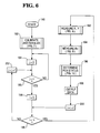
- Fig. 6 a method for determining touch position is disclosed, beginning with START 180.
- the vertical ITO strips are labeled Y0, Y1, Y2,..., Ym, starting from the left side of digitizer 12.
- the horizontal ITO strips are labeled X0, X1,..., Xn, starting from the bottom side of digitizer 12.
- the left and bottom sides of each ITO strip are referred to as the "-" or "negative” sides, while the top and right sides of each ITO strip are referred to as the "+" or "positive” sides.
- controller 14 performs a calibration and initialization step. Controller 14 then steps through each segment intersection of the digitizer and determines position, contact resistance, and pen status. It does this by first initializing count variable j to 0 in step 184.
- step 186 controller 14 determines whether count variable j is less than horizontal constant n. If count variable j is not less than horizontal constant n, the procedure returns to step 184. Otherwise, the procedure continues to step 188 where controller 14 sets count variable i to zero.
- Controller 14 determines whether count variable i is less than vertical constant m in step 190. If count variable i is not less than vertical constant m, then the procedure branches to step 202, where count variable j is incremented by one and the procedure continues at step 186. Otherwise, operation continues to step 192.
- step 192 controller 14 measures position.
- step 194 controller 14 measures contact resistance Rc at the point of actuation.
- controller 14 determines whether the writing instrument is up, down, or in a multipoint condition in step 196.
- step 198 controller 14 outputs contact resistance Rc, pen status, and position to host system 24 via interface 22.
- controller 14 increments count variable i in step 200 and returns to step 190.
- calibration means creating a mapping function between real world and digitized positional coordinates.
- Real world coordinates represent actual physical locations
- digitizer coordinates represent real world coordinates as measured by the digitizer.
- the calibration mapping function ideally corrects for four types of differences between real world and digitizer coordinate systems: offset, scale, skew, and distortion.
- Offset is caused by a misalignment of absolute origins between real world and digitizer coordinate systems, while scale is caused by different distances per coordinate count between the two coordinate systems.
- Skew is caused by an apparent rotation between the two coordinate systems, and distortion is caused by nonlinearities in the digitizer sampling function.
- Controller 14 individually calibrates each segment. If the calibration mapping function is not accurate from segment to segment, there will be an apparent discontinuity in the digitized positional coordinates when a stylus or finger crosses from one segment to another.
- x_max is the real world x-location of the positive end of ITO strip Xj
- x_max' is the digitized x-location of the positive end of ITO strip Xj
- y_max is the real world y-location of the positive end of ITO strip Yi
- y_max' is the digitized y-location of the positive end of ITO strip Yi
- x_min is the real world x-location of the negative end of ITO strip Xj
- x_min' is the digitized x-location of the negative end of ITO strip Yi
- y_min' is the digitized y-location of the negative end of ITO strip Yi.
- Controller 14 uses equations 7, 8, 9, and 10 to calculate constants m_x, m_y, b_x, and b_y.
- controller 14 automatically calibrates digitizer 12 for accuracy and also takes several baseline readings required to calculate contact resistance Rc in later steps of Fig. 6.
- controller 14 initializes the index variable j to zero in step 206.
- controller 14 determines whether count variable j is less than horizontal constant n. If count variable j is less than horizontal constant n, controller 14 continues to step 210 where it energizes ITO strip Xj. This means applying voltage source 56 to the positive end of the segment and ground 60 to the negative end of the segment. For ITO strip X0 (ITO strip 162), controller 14 would do this by closing analog switches 48, 40, and 52 while leaving all other switches open. If count variable j is not less than horizontal constant n, then the method proceeds to step 224.
- controller 14 measures the quantities x_max' and x_min' at the positive and negative ends of the energized ITO strip Xj.
- controller 14 selects voltage sense point 82 through multiplexer 26, reads x_max' from A/D converter 28, selects voltage sense point 90 through multiplexer 26, and then reads x_min' from A/D converter 28.
- controller 14 calculates the scalar constant m_x[j] using equation (7) above.
- Scalar matrix m_x[] is an n-long array for storing the m_x scalar constants for each Xj electrode.
- controller 14 calculates the offset constant b_x[j] in step 216 using equation (8) above.
- controller 14 sets up to read voltage Vx[j] and then takes the actual reading in step 220. Controller 14 requires voltage Vx to calculate contact resistance Rc. To measure voltage Vx[j], controller 14 measures the voltage required to inject a constant current into the positive end of the segment Xj while grounding the negative end. For ITO strip X0 (ITO strip 162), controller 14 closes analog switches 40, 48, and 54 while leaving all other switches open. Controller 14 then selects voltage sense point 82 through multiplexer 26 and measures voltage Vx[0] at A/D converter 28.
- step 222 controller 14 increments count variable j by one and then returns to step 208.
- step 208 if count variable j is not less than horizontal constant n, operation continues to step 224 where controller 14 sets count variable i to 0.
- controller 14 determines whether count variable i is less than vertical constant m. If count variable i is less than vertical constant m, the procedure continues to step 230 where controller 14 energizes ITO strip Yi. For ITO strip Y0 (ITO strip 130) controller 14 closes analog switches 32, 46, and 52 while leaving all other switches open.
- controller 14 measures the quantities y_max and y_min at the positive and negative ends respectively of the energized ITO strip Yi.
- controller 14 selects voltage sense point 74 through multiplexer 26, reads y_max from A/D converter 28, selects voltage sense point 88 through multiplexer 26, and reads y_min from A/D converter 28.
- controller 14 calculates the scalar constant m_y[i] using equation (9) above. Similarly, controller 14 calculates the offset constant b_y[i] in step 236 using equation (10) above.
- Controller 14 sets up to read voltage Vy[i] in step 238 and makes the actual reading in step 240. Controller 14 requires voltage Vy to calculate contact resistance Rc. To measure voltage Vy[i], controller 14 measures the voltage required to inject a constant current into the positive end of the segment Yi while grounding the negative end. For ITO strip Y0 (ITO strip 130), controller 14 closes analog switches 32, 46, and 54 while leaving all other switches open. Controller 14 then selects voltage sense point 74 through multiplexer 26 and measures voltage Vy[0] at A/D converter 28.
- step 242 controller 14 increments count variable i by one and returns to step 226.
- controller 14 is finished initializing and calibrating and proceeds to step 184 of Fig. 6 via step 228.
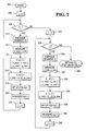
- controller 14 charges the ITO strip Yi by charging the digitizer as well as the low pass filters for segment Yi to voltage source 56.
- controller 14 closes switches 32 and 52 for a short period of time while leaving all other switches open.
- step 254 controller 14 energizes segment Xj.
- step 256 controller 14 waits for the opposite layer segment Yi to discharge to the positional voltage at the point of actuation.
- controller 14 measures the temporary quantity x_pos at segment Yi. For Y0 (ITO strip 130), controller 14 selects voltage sense point 74 and measure x_pos at A/D converter 28.
- controller 14 discharges segment Yi by discharging the digitizer as well as the low pass filter for ITO strip Yi.
- controller 14 closes switch 46 for a short period of time while leaving all other switches open.
- step 262 controller 14 energizes ITO strip Xj.
- step 264 controller 14 waits, just as in the previous step 256.
- controller 14 measures x_neg in exactly the same way it measured x_pos in step 258.
- controller 14 calculates position by applying the calibration mapping function (equation (1) above) to the average of x_pos and x_neg.
- controller 14 charges ITO strip Xj by connecting ITO strip Xj and associated low pass filters to voltage source 56.
- ITO strip X0 ITO strip 14
- controller 14 closes switches 40 and 52 for a short period of time while leaving all other switches open.
- controller 14 energizes segment Yi just as in step 230 of Fig. 7.
- Controller 14 waits for the opposite layer segment Xj to discharge to the positional voltage at the point of actuation in step 274.
- controller 14 measures the temporary quantity y_pos at segment Xj.
- controller 14 selects voltage sense point 82 through multiplexer 26 and measures y_pos at A/D converter 28.
- controller 14 discharges segment Xj to ground 60.
- controller 14 closes switch 48 for a short period of time while leaving all other switches open.
- Controller 14 then energizes segment Yi in step 280 and waits in step 282, just as in the previous steps 272 and 274.
- Controller 14 measures y_neg in step 284 in exactly the same way it measured y_pos in step 276.
- step 288 the procedure ends by returning to step 194 of Fig. 6.
- Contact resistance Rc is the resistance between the two conductive layers 118 and 120 at the point of actuation exclusive of the resistance of the layers themselves.
- controller 14 sets up to measure V1 for the segment pair Xj, Yi. Controller 14 measures the voltage V1 required to drive a constant current into segment Xj, through the contact resistance Rc at the point of actuation, into ITO strip Yi, and back to ground 60. For the segment pair X0 (ITO strip 14), Y0 (ITO strip 130), controller 14 closes switches 32, 48, and 54 while leaving all other switches open.
- controller 14 reads voltage V1 at the positive end of segment Xj.
- controller 14 reads voltage point 74 through multiplexer 26 and A/D converter 28.
- controller 14 sets up to read voltage V2 for the segment pair Xj, Yi. Controller 14 measures the voltage required to drive a constant current into segment Yi, through the contact resistance Rc at the point of actuation, into segment Xj, and then into ground 60. For segment pair X0 (ITO strip 14), Y0 (ITO strip 130), controller 14 closes switches 40, 46, and 54 while leaving all other switches open.
- controller 14 reads voltage V2 at the positive end of segment Yi. For segment pair X0 (ITO strip 14), Y0 (ITO strip 130), controller 14 selects voltage sense point 82 through multiplexer 26 and A/D converter 28.
- step 302 the procedure returns to step 196 of Fig. 6.
- Controller 14 determines pen status according to a combination of Rc, x_pos, x_neg, y_pos, and y_neg.
- step 306 controller 14 determines whether the absolute value of the difference between x_pos and x_neg is less than x_thresh, where x_thresh is a threshold constant typically on the order of four counts for a 10-bit A/D converter 28. If decision step 306 is not true, then the x coordinate is not stable and operation continues to step 308 where controller 14 sets the pen status to UP, meaning a stylus or finger is not contacting digitizer 12. After step 308, operation returns in step 310 to step 198 of Fig. 6.
- step 312 controller 14 determines whether the absolute value of y_pos minus y_neg is less than y_thresh.
- y_thresh is a threshold constant typically on the order of four counts for a 10-bit A/D converter 28. If this is not true, the y coordinate is not stable and execution continues at step 308. Otherwise, execution continues to step 314 where controller 14 determines whether contact resistance Rc is less than threshold constant Rc_down. Threshold constant Rc_down is typically on the order of 90% of the full scale contact resistance Rc reading.
- step 308 If contact resistance Rc is not less than threshold constant Rc_down, then execution continues to step 308. Otherwise, execution continues to step 316 where controller 14 determines whether contact resistance Rc is less than threshold constant Rc_multipoint.
- Rc_multipoint is typically on the order of 10% of the full scale contact resistance Rc reading.
- step 318 controller 14 sets the pen status to MULTIPOINT. This means that the user is touching digitizer 12 with a finger.
- step 316 if contact resistance Rc is not less than threshold constant Rc_multipoint, controller 14 sets the pen status to DOWN in step 320. This means that only the stylus is actuating digitizer 12. In either case 318 or 320, execution continues to step 310 where the procedure returns to step 198 of Fig. 6.
- system 10 and segmented digitizer 12 of the present invention solve the problems associated with conventional four wire membrane digitizers while adding the extra feature of multipoint detection.
- Multipoint detection means that segmented digitizer 12 can not only track a writing instrument, such as a stylus, while the user is touching with a finger, but can individually determine the positions of two or more objects touching digitizer 12 at the same time. This feature could be used to emulate a mouse button function in one area of the digitizer 12 while emulating a mouse position function in another area.
- segmented digitizer 12 Another benefit of segmented digitizer 12 is decreased power consumption. Dividing the digitizer into segments increases its effective resistance. The higher the resistance, the lower the current required to drive it, and the less power it consumes. Decreased power consumption is important in today's battery powered handwriting capture devices.
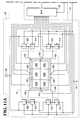
- Figs. 11A and 1B the second embodiment of the system of Fig. 1 is shown in more detail.
- the second embodiment is based upon a five-wire segmented digitizer. Differences between the four-wire system and the five-wire system are discussed below.
- Analog processing circuitry 13 preferably includes multiplexer 26, analog switches 402, 404, and 406, filter 400, and analog-to-digital (A/D) converter 28.
- Controller 14 reads the voltages at segments 408a-f through A/D converter 28.
- Multiplexer 26 multiplexes signals from segments 408a-f.
- A/D converter 28 converts the analog signals from each of segments 408a-f into digital numbers.
- Analog processing circuitry 13 also includes filter 400, which removes any electrical noise that might be present from segmented digitizer 12.
- Filter 400 may be a standard first order filter.
- Controller 14 may preset the initial conditions for filter 400 using analog switches 402-406.
- Drive circuitry 20 includes analog switches 410-424, which apply either voltage source 50, or electrical ground 60 to the corners 414-436 of electrode ring 438, in accordance with instructions from controller 14.
- Drive circuitry 20 also includes current source 427 and analog switch 425 for selectively applying current I to a given segment 408a-f through multiplexer 26.
- Analog switches 410-425 are standard single pole, single throw, digitally controlled analog switches.
- segmented digitizer 12 is shown as a segmented five wire membrane digitizer.
- Digitizer 12 includes several layers of polyester and adhesive attached to a rigid substrate. Conductors are silk-screened with silver ink, while various surfaces of digitizer 12 are coated with indium tin oxide (ITO), a transparent conductor. Digitizer 12 connects to other components of circuit 10 via a flat flex connector tail 114.
- ITO indium tin oxide
- the cross sectional view in Fig. 3 also applies to the segmented five-wire membrane digitizer of Figs. 12 and 13.
- top layer 116 is shown in more detail.
- Top layer 116 includes ITO strips 457-462. Electrodes 463-468 make electrical contact with ITO strips 457-462, respectively.
- Bottom layer 122 is shown in more detail.
- Bottom layer 122 consists primarily of ITO area 440 surrounded by electrode pattern 438.
- Electrode pattern 438 is typically a special silk-screened pattern of silver ink, as described in U.S. Patent No. 4,371,746 to Pepper. Alternatively, it can be a ring of discrete resistors, discrete diodes, spot electrodes, bar electrodes, or a solid band of moderate resistance conductive ink. Silver ink traces 442-448 contact the electrode pattern 438 at its corners.
- Calibration sense points 454-456 detect the actual voltage along the edges of ITO area 440.
- U.S. Patent No. 4,435,616 by Kley details one way of constructing calibration sense points 450-456.
- calibration sense points 450-456 could simply contact the midpoints of the electrode pattern detailed in the above mentioned U.S. Patent No. 4,371,746.
- top layer 116 Placement of top layer 116 over bottom layer 122 effectively creates six separate writing areas corresponding to segments 408a-f.
- ITO strips 457-462 are numbered 0, 1, 2, ..., m ⁇ n, starting from the lower left hand corner of the segmented digitizer 12 and moving bottom to top, left to right.
- ITO strips 457-462 are numbered 0, 1, 2, 3, 4, and 5, respectively.
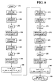
- controller 14 performs a calibration and initialization step. Controller 14 then steps through each segment of the digitizer 12 and determines position, contact resistance Rc, and pen status. It does this by first initializing count variable k to 0 in step 474.
- step 476 controller 14 determines whether count variable k is less than the number of segments, m ⁇ n. If count variable k is not less than horizontal constant m ⁇ n, the procedure returns to step 474. Otherwise, the procedure continues to step 478.
- controller 14 measures position.
- controller 14 measures contact resistance Rc at the point of actuation.
- controller 14 determines whether the writing instrument is up, down, or in a multipoint condition in step 482.
- controller 14 outputs contact resistance Rc, pen status, and position to host system 24 via interface 22.
- controller 14 increments count variable k in step 486 and returns to step 476.
- Fig. 15 the calibration and initialization step 472 from Fig. 13 is shown in more detail.
- the calibration procedure and equations are similar to those of the first embodiment. Good calibration is not as important in the second embodiment because unlike the first embodiment there is no inherent problem with segment mismatch.
- the calibration and initialization procedure begins at START 490
- controller 14 drives segmented digitizer 12 in the x-direction. Controller 14 closes switches 406, 424, 410, 416, and 420 while leaving all other switches open. This creates a voltage gradient along back layer 122 of digitizer 12 that increases from left to right.
- controller 14 measures x_max' and x_min' at calibration sense points 454 and 450 respectively. Controller 14 selects each calibration sense point in turn through multiplexer 26 and reads the resulting value from A/D converter 28.
- controller 14 calculates the scalar constant m_x using equation (7) from above. Similarly, controller 14 calculates the offset constant b_x in step 498 using equation (8) from above.
- controller 14 drives segmented digitizer 12 in the y-direction. Controller 14 closes switches 406, 422, 420, 410, and 413 while leaving all other switches open. This creates a voltage gradient along back layer 122 of digitizer 12 that increases from bottom to top.
- controller 14 measures y_max' and y_min' at calibration sense points 452 and 456 respectively. Controller 14 selects each calibration sense point in turn through multiplexer 26 and reads the resulting value from A/D converter 28.
- controller 14 calculates the scalar constant m_y using equation (9) from above. Similarly, controller 14 calculates the offset constant b_y in step 506 using equation (10) from above.
- controller 14 returns to step 474 of Fig. 14 in step 508.
- controller 14 charges ITO strip Sk by applying voltage source 50 to digitizer 12 and low pass filter 400. Controller 14 selects ITO strip Sk (ITO strip 457) through multiplexer 26 and closes switches 402 and 406 for a short period of time while leaving all other switches open.
- controller 14 drives the segmented digitizer 12 in the x-direction just as in step 492 from Fig. 15.
- controller 14 waits for ITO strip Sk to discharge to the positional voltage at the point of actuation.
- controller 14 measures the temporary quantity x_pos at segment Sk. Controller 14 selects ITO strip Sk (ITO strip 457) through multiplexer 26 and measure x_pos at A/D converter 28.
- controller 14 discharges ITO strip Sk by discharging digitizer 12 andlow pass filter 400. Controller 14 selects ITO strip Sk (ITO strip 457) through multiplexer 26 and closes switches 404 and 406 for a short period of time while leaving all other switches open.
- controller 14 drives segmented digitizer 12 in the x-direction just as in step 492 from Fig. 15.
- step 524 controller 14 waits, just as in the previous step 516.
- controller 14 measures x_neg in exactly the same way it measured x_pos in step 518.
- controller 14 calculates position by applying the calibration mapping function (equation (1) above) to the average of x_pos and x_neg.
- controller 14 charges ITO strip Sk just as in previous step 512.
- controller 14 drives the segmented digitizer 12 in the y-direction just as in step 500 from Fig. 15.
- step 534 controller 14 waits, just as in the previous step 516.
- controller 14 measures the temporary quantity y_pos at ITO strip Sk using the same procedure as in the previous step 518.
- controller 14 charges ITO strip Sk just as in previous step 512.
- controller 14 drives the segmented digitizer 12 in the y-direction just as in step 500 from Fig. 15.
- step 542 controller 14 waits, just as in the previous step 516.
- controller 14 measures the temporary quantity y_neg at ITO strip Sk using the same procedure as in the previous step 526.
- step 548 the procedure ends by returning to step 480 of Fig. 14.
- Fig. 17 the method of determining contact resistance Rc is discussed in detail, beginning with START 550.
- controller 14 selects ITO strip Sk through multiplexer 26 and closes switches 406, 425, 410, 424, 418, and 414 while leaving all other switches open. This grounds all corners of the electrode pattern 438 through silver ink traces 442-448 and injects a constant current I from current source 427 into ITO strip Sk through multiplexer 26.
- step 554 controller 14 actually measures the resulting contact resistance Rc for segment Sk at A/D converter 28.
- step 556 controller 14 returns to step 482 in Fig. 14.
- Fig. 19 a schematic representation of digitizer 22 is shown, depicting the digitizer drive circuitry 20 as it is set in step 552 of Fig. 17.
- Resistors 588-594 represent the resistances from the point of actuation on bottom digitizer layer 122 to each corner 414-436 of electrode pattern 438 respectively.
- Resistance 584 represents the resistance from the point of actuation on ITO strip Sk to the corresponding segment Sk electrode.
- Voltage V1 is the voltage at the output of multiplexer 26.
- V1 is approximately equal to the product I ⁇ Rc. If current I is constant, voltage V1 is directly proportional to contact resistance Rc. Because controller 14 is not concerned with the absolute resistance, it can treat voltage V1 as if it were contact resistance Rc, even though it is only proportional to contact resistance Rc.
- Controller 14 determines pen status according to a combination of contact resistance Rc, x_pos, x_neg, y_pos, and y_neg.
- step 562 controller 14 determines whether the absolute value of the difference between x_pos and x_neg is less than x_thresh, where x_thresh is a threshold constant typically on the order of four counts for a 10-bit A/D converter. If decision step 562 is not true, then the x coordinate is not stable and operation continues to step 574 where controller 14 sets the pen status to UP, meaning a stylus or finger is not contacting digitizer 12. After step 574, operation returns in step 576 to step 484 of Fig. 14.
- step 564 controller 14 determines whether the absolute value of y_pos minus y_neg is less than y_thresh.
- y_thresh is a threshold constant typically on the order of four counts for a 10-bit A/D converter. If this is not true, the y-coordinate is not stable and execution continues at step 574. Otherwise, execution continues to step 566 where controller 14 determines whether contact resistance Rc is less than threshold constant Rc_down. Threshold constant Rc_down is typically on the order of 90% of the full scale contact resistance Rc reading.
- step 574 If contact resistance Rc is not less than threshold constant Rc_down, then execution continues to step 574. Otherwise, execution continues to step 568 where controller 14 determines whether contact resistance Rc is less than threshold constant Rc_multipoint.
- Rc_multipoint is typically on the order of 10% of the full scale contact resistance Rc reading.
- step 570 controller 14 sets the pen status to MULTIPOINT. Therefore, a user is touching digitizer 12 with a finger.
- step 568 if contact resistance Rc is not less than threshold constant Rc_multipoint, controller 14 sets the pen status to DOWN in step 572. Therefore, only a stylus is actuating digitizer 12. In either case 570 or 572, execution continues to step 576 where the procedure returns to step 484 of Fig. 14.
Landscapes
- Engineering & Computer Science (AREA)
- General Engineering & Computer Science (AREA)
- Theoretical Computer Science (AREA)
- Human Computer Interaction (AREA)
- Physics & Mathematics (AREA)
- General Physics & Mathematics (AREA)
- Position Input By Displaying (AREA)
- Image Input (AREA)
- User Interface Of Digital Computer (AREA)
Applications Claiming Priority (2)
| Application Number | Priority Date | Filing Date | Title |
|---|---|---|---|
| US80278 | 1993-06-21 | ||
| US08/080,278 US5412161A (en) | 1993-06-21 | 1993-06-21 | Handwriting capture system with segmented digitizer |
Publications (3)
| Publication Number | Publication Date |
|---|---|
| EP0631256A2 true EP0631256A2 (fr) | 1994-12-28 |
| EP0631256A3 EP0631256A3 (fr) | 1998-12-16 |
| EP0631256B1 EP0631256B1 (fr) | 2001-09-05 |
Family
ID=22156363
Family Applications (1)
| Application Number | Title | Priority Date | Filing Date |
|---|---|---|---|
| EP94304376A Expired - Lifetime EP0631256B1 (fr) | 1993-06-21 | 1994-06-16 | Dispositif d'entrée du type digitaliseur |
Country Status (4)
| Country | Link |
|---|---|
| US (2) | US5412161A (fr) |
| EP (1) | EP0631256B1 (fr) |
| JP (1) | JPH07146745A (fr) |
| DE (1) | DE69428164T2 (fr) |
Cited By (12)
| Publication number | Priority date | Publication date | Assignee | Title |
|---|---|---|---|---|
| WO1998049650A1 (fr) * | 1997-04-25 | 1998-11-05 | Raychem Limited | Convertisseur pour ecrans tactiles resistifs |
| EP0965116A4 (fr) * | 1996-04-12 | 2001-01-03 | Elo Touchsystems Inc | Ecran tactile resistant presentant des zones multiples de selection au moyen d'une discrimination par la pression |
| US6278444B1 (en) | 1998-08-21 | 2001-08-21 | Geoffrey D. Wilson | Low current four-wire interface for five-wire resistive touch-screen |
| US6506983B1 (en) | 1996-03-15 | 2003-01-14 | Elo Touchsystems, Inc. | Algorithmic compensation system and method therefor for a touch sensor panel |
| WO2003030091A1 (fr) * | 2001-10-03 | 2003-04-10 | 3M Innovative Properties Company | Systeme de panneau tactile et procede permettant de distinguer des touches de saisie tactiles multiples |
| WO2004027593A3 (fr) * | 2002-09-17 | 2004-08-12 | Elo Touchsystems Inc | Corrections dynamiques pour ecran tactile non lineaire |
| EP1277197A4 (fr) * | 1999-12-06 | 2007-02-28 | Elo Touchsystems Inc | Ecran tactile am liore a grille relativement conductrice |
| EP1126406A3 (fr) * | 2000-02-10 | 2008-04-02 | Nec Corporation | Dispositif d'entrée à écran tactile |
| EP2075679A1 (fr) | 2007-12-19 | 2009-07-01 | ASUSTeK Computer Inc. | Panneau tactile |
| US8395592B2 (en) | 2008-08-05 | 2013-03-12 | Apex Material Technology Corp. | Sensing system |
| US8493355B2 (en) | 2008-05-14 | 2013-07-23 | 3M Innovative Properties Company | Systems and methods for assessing locations of multiple touch inputs |
| EP2244173A3 (fr) * | 2009-04-22 | 2014-09-24 | Fujitsu Component Limited | Procédé de détection de position pour panneau d'écran tactile, panneau d'écran tactile et appareil électronique |
Families Citing this family (30)
| Publication number | Priority date | Publication date | Assignee | Title |
|---|---|---|---|---|
| US6005200A (en) * | 1994-08-05 | 1999-12-21 | Hyundai Electronics America | Compensation of stylus signals in digitizing tablet |
| US6262719B1 (en) * | 1994-09-02 | 2001-07-17 | Packard Bell Nec, Inc. | Mouse emulation with a passive pen |
| US5734129A (en) * | 1994-09-23 | 1998-03-31 | Belville; Daniel T. | Forms for use with handwriting capturing device |
| US6963783B1 (en) * | 1995-10-16 | 2005-11-08 | Packard Bell Nec | Audio compression in a wireless remote interface tablet |
| US5892824A (en) * | 1996-01-12 | 1999-04-06 | International Verifact Inc. | Signature capture/verification systems and methods |
| US6650319B1 (en) | 1996-10-29 | 2003-11-18 | Elo Touchsystems, Inc. | Touch screen based topological mapping with resistance framing design |
| JPH10240424A (ja) * | 1997-02-21 | 1998-09-11 | Alps Electric Co Ltd | 座標入力装置 |
| US6779178B1 (en) | 1997-03-07 | 2004-08-17 | Signature Mail. Com, Llc | System and method for personalizing electronic mail messages |
| US6278068B1 (en) * | 1998-03-09 | 2001-08-21 | Tritech Microelectronics, Inc. | Integrated technique for filtering and measuring signals of four and five wire digitizers |
| US6355895B1 (en) | 1998-10-26 | 2002-03-12 | Greensteel, Inc. | Spacing structures for large touch panels |
| US6738048B1 (en) * | 1999-10-29 | 2004-05-18 | Texas Instruments Incorporated | Touch screen controller |
| US6603464B1 (en) | 2000-03-03 | 2003-08-05 | Michael Irl Rabin | Apparatus and method for record keeping and information distribution |
| US6621486B2 (en) * | 2001-01-23 | 2003-09-16 | Mobigence, Inc. | Expanded touch panel display |
| TW571227B (en) * | 2002-09-09 | 2004-01-11 | Sunplus Technology Co Ltd | Panel sensing device and its positioning location searching method |
| US20050276454A1 (en) * | 2004-06-14 | 2005-12-15 | Rodney Beatson | System and methods for transforming biometric image data to a consistent angle of inclination |
| US7113179B2 (en) * | 2004-06-23 | 2006-09-26 | Interlink Electronics, Inc. | Force sensing resistor with calibration element and method of manufacturing same |
| JP2007303874A (ja) * | 2006-05-09 | 2007-11-22 | Fujitsu Ltd | 電源センス回路,電源供給システム,及び集積回路 |
| US8355009B2 (en) * | 2007-04-25 | 2013-01-15 | Mcdermid William J | Method and apparatus for determining coordinates of simultaneous touches on a touch sensor pad |
| JP5136086B2 (ja) * | 2008-01-28 | 2013-02-06 | パナソニック株式会社 | タッチパネル |
| US20090322701A1 (en) * | 2008-06-30 | 2009-12-31 | Tyco Electronics Corporation | Method and apparatus for detecting two simultaneous touches and gestures on a resistive touchscreen |
| TWI459251B (zh) * | 2009-05-21 | 2014-11-01 | Apex Material Technology Corp | 感知系統以及用於該感知系統的訊號處理方法 |
| TWI393044B (zh) * | 2008-08-05 | 2013-04-11 | Salt Internat Corp | 適用於電阻式觸控螢幕之控制電路 |
| JP5397979B2 (ja) * | 2008-09-10 | 2014-01-22 | 株式会社ジャパンディスプレイ | 抵抗膜型入力装置、入力機能付き表示装置および電子機器 |
| US8345019B2 (en) | 2009-02-20 | 2013-01-01 | Elo Touch Solutions, Inc. | Method and apparatus for two-finger touch coordinate recognition and rotation gesture recognition |
| CN101989143B (zh) * | 2009-07-31 | 2013-05-01 | 群康科技(深圳)有限公司 | 触控装置及其控制方法 |
| JP5566676B2 (ja) * | 2009-12-18 | 2014-08-06 | 富士通コンポーネント株式会社 | タッチパネル、及びタッチパネルの座標検出方法 |
| TWI403935B (zh) * | 2010-03-29 | 2013-08-01 | Apex Material Technology Corp | 觸控面板 |
| JP2012088762A (ja) | 2010-10-15 | 2012-05-10 | Touch Panel Systems Kk | タッチパネル入力装置およびジェスチャ検出方法 |
| CN104133708A (zh) * | 2014-08-05 | 2014-11-05 | 广州市思码触屏科技有限公司 | 一种电阻式多点触摸计算机操作系统 |
| JP6727072B2 (ja) * | 2016-08-24 | 2020-07-22 | ローム株式会社 | 抵抗膜タッチパネルの制御回路、タッチ式入力装置 |
Family Cites Families (20)
| Publication number | Priority date | Publication date | Assignee | Title |
|---|---|---|---|---|
| US4386232A (en) * | 1981-06-16 | 1983-05-31 | Foster Wheeler Energy Corporation | Multiplexed touch sensitive screen system |
| JPS5884339A (ja) * | 1981-11-14 | 1983-05-20 | Pentel Kk | タブレツト入力装置 |
| JPS594382A (ja) * | 1982-06-30 | 1984-01-11 | Nippon Telegr & Teleph Corp <Ntt> | 描画像の符号化方式 |
| US4755634A (en) * | 1983-07-12 | 1988-07-05 | Peptek, Incorporated | Conductive electrode arrays and arrays of resistive elements for use in touch panels and for producing electric fields |
| JPS6039232A (ja) * | 1983-08-12 | 1985-03-01 | Nippon Telegr & Teleph Corp <Ntt> | タブレツト |
| JPS60131041U (ja) * | 1984-02-08 | 1985-09-02 | シャープ株式会社 | 手書き入力情報の処理装置 |
| US4625075A (en) * | 1984-09-25 | 1986-11-25 | Sierracin Corporation | Patterned conductive ink touch panel |
| US4707570A (en) * | 1985-02-12 | 1987-11-17 | Ricoh Company, Ltd. | Manual information input device |
| US4638118A (en) * | 1985-03-11 | 1987-01-20 | Wang Laboratories, Inc. | Writing pad |
| US4739299A (en) * | 1986-01-17 | 1988-04-19 | Interlink Electronics, Inc. | Digitizer pad |
| US4745242A (en) * | 1986-02-10 | 1988-05-17 | Omron Tateisi Electronics Co. | Coordinate input sheet with correction electrodes |
| US4801771A (en) * | 1986-10-13 | 1989-01-31 | Yamaha Corporation | Force sensitive device |
| JPH02178822A (ja) * | 1988-12-29 | 1990-07-11 | Toppan Moore Co Ltd | 信号入力シート |
| US5278399A (en) * | 1989-03-28 | 1994-01-11 | Toppan Moore Company, Ltd. | Data entry unit |
| US5045643A (en) * | 1989-06-19 | 1991-09-03 | Brother Kogyo Kabushiki Kaisha | Positional information inputting device using sheet-like photo-conductive switch or the like |
| US5465103A (en) * | 1989-08-28 | 1995-11-07 | Mitsubishi Denki Kabushiki Kaisha | Display device with coordinate input function |
| US5049862A (en) * | 1989-10-06 | 1991-09-17 | Communication Intelligence Corporation ("Cic") | Keyless flat panel portable computer--computer aided notebook |
| JPH0468392A (ja) * | 1990-07-09 | 1992-03-04 | Toshiba Corp | 画像表示装置 |
| US5149918A (en) * | 1990-10-29 | 1992-09-22 | International Business Machines Corporation | Touch sensitive overlay |
| JP2584535B2 (ja) * | 1990-11-29 | 1997-02-26 | シャープ株式会社 | タッチパネル入力方法 |
-
1993
- 1993-06-21 US US08/080,278 patent/US5412161A/en not_active Expired - Lifetime
-
1994
- 1994-06-16 DE DE69428164T patent/DE69428164T2/de not_active Expired - Lifetime
- 1994-06-16 EP EP94304376A patent/EP0631256B1/fr not_active Expired - Lifetime
- 1994-06-20 JP JP13676194A patent/JPH07146745A/ja active Pending
-
1995
- 1995-04-17 US US08/400,733 patent/US5563381A/en not_active Expired - Lifetime
Cited By (20)
| Publication number | Priority date | Publication date | Assignee | Title |
|---|---|---|---|---|
| US6506983B1 (en) | 1996-03-15 | 2003-01-14 | Elo Touchsystems, Inc. | Algorithmic compensation system and method therefor for a touch sensor panel |
| EP0965116A4 (fr) * | 1996-04-12 | 2001-01-03 | Elo Touchsystems Inc | Ecran tactile resistant presentant des zones multiples de selection au moyen d'une discrimination par la pression |
| US6373475B1 (en) | 1997-04-25 | 2002-04-16 | Michael Challis | Converter for resistive touchscreens |
| WO1998049650A1 (fr) * | 1997-04-25 | 1998-11-05 | Raychem Limited | Convertisseur pour ecrans tactiles resistifs |
| US6278444B1 (en) | 1998-08-21 | 2001-08-21 | Geoffrey D. Wilson | Low current four-wire interface for five-wire resistive touch-screen |
| EP1277197A4 (fr) * | 1999-12-06 | 2007-02-28 | Elo Touchsystems Inc | Ecran tactile am liore a grille relativement conductrice |
| US7800589B2 (en) | 1999-12-06 | 2010-09-21 | Tyco Electronics Corporation | Touch screen with relatively conductive grid |
| EP1126406A3 (fr) * | 2000-02-10 | 2008-04-02 | Nec Corporation | Dispositif d'entrée à écran tactile |
| EP1843244A2 (fr) | 2001-10-03 | 2007-10-10 | 3M Innovative Properties Company | Système de panneau tactile et procédé de distinction d'entrées de touches multiples |
| US7254775B2 (en) | 2001-10-03 | 2007-08-07 | 3M Innovative Properties Company | Touch panel system and method for distinguishing multiple touch inputs |
| EP1843244A3 (fr) * | 2001-10-03 | 2007-12-12 | 3M Innovative Properties Company | Système de panneau tactile et procédé de distinction d'entrées de touches multiples |
| WO2003030091A1 (fr) * | 2001-10-03 | 2003-04-10 | 3M Innovative Properties Company | Systeme de panneau tactile et procede permettant de distinguer des touches de saisie tactiles multiples |
| US7180508B2 (en) | 2002-09-17 | 2007-02-20 | Tyco Electronics Corporation | Dynamic corrections for a non-linear touchscreen |
| WO2004027593A3 (fr) * | 2002-09-17 | 2004-08-12 | Elo Touchsystems Inc | Corrections dynamiques pour ecran tactile non lineaire |
| EP2075679A1 (fr) | 2007-12-19 | 2009-07-01 | ASUSTeK Computer Inc. | Panneau tactile |
| US8493355B2 (en) | 2008-05-14 | 2013-07-23 | 3M Innovative Properties Company | Systems and methods for assessing locations of multiple touch inputs |
| US8395592B2 (en) | 2008-08-05 | 2013-03-12 | Apex Material Technology Corp. | Sensing system |
| EP2244173A3 (fr) * | 2009-04-22 | 2014-09-24 | Fujitsu Component Limited | Procédé de détection de position pour panneau d'écran tactile, panneau d'écran tactile et appareil électronique |
| US9280249B2 (en) | 2009-04-22 | 2016-03-08 | Fujitsu Component Limited | Position detecting method for touchscreen panel, touchscreen panel, and electronic apparatus |
| US10095365B2 (en) | 2009-04-22 | 2018-10-09 | Fujitsu Component Limited | Position detecting method for touchscreen panel, touchscreen panel, and electronic apparatus |
Also Published As
| Publication number | Publication date |
|---|---|
| US5412161A (en) | 1995-05-02 |
| EP0631256A3 (fr) | 1998-12-16 |
| US5563381A (en) | 1996-10-08 |
| EP0631256B1 (fr) | 2001-09-05 |
| DE69428164D1 (de) | 2001-10-11 |
| DE69428164T2 (de) | 2002-06-06 |
| JPH07146745A (ja) | 1995-06-06 |
Similar Documents
| Publication | Publication Date | Title |
|---|---|---|
| EP0631256B1 (fr) | Dispositif d'entrée du type digitaliseur | |
| CA1241754A (fr) | Systeme et methode d'electrophotographie | |
| US7148704B2 (en) | Charge transfer capacitive position sensor | |
| US4678869A (en) | Position responsive apparatus, system and method having electrographic application | |
| US8508502B2 (en) | Capacitive touchscreen system with touch position encoding during analog-to-digital conversion | |
| US8355009B2 (en) | Method and apparatus for determining coordinates of simultaneous touches on a touch sensor pad | |
| WO2004027593A2 (fr) | Corrections dynamiques pour ecran tactile non lineaire | |
| TWI433014B (zh) | 顯示裝置 | |
| US20080100586A1 (en) | Method and system for calibrating a touch screen | |
| US6278444B1 (en) | Low current four-wire interface for five-wire resistive touch-screen | |
| US6016140A (en) | Automatic touch screen calibration | |
| US20090314551A1 (en) | Touch panel | |
| CN101089802A (zh) | 二维位置传感器 | |
| EP0155781A1 (fr) | Appareil détecteur de coordonnées | |
| US20150009180A1 (en) | Two-Dimensional Touch Panel | |
| EP2204726A1 (fr) | Contrôleur d'écran tactile | |
| US10990236B2 (en) | Methods for two-touch detection with resistive touch sensor and related apparatuses and systems | |
| US5367130A (en) | Graphics tablet scanning and error reduction | |
| US9507454B1 (en) | Enhanced linearity of gestures on a touch-sensitive surface | |
| US6151013A (en) | Electrical probe-position sensor | |
| CA1228905A (fr) | Systeme de visualisation interactif | |
| KR100949217B1 (ko) | 아날로그-디지털 하이브리드 터치패널장치 및 그 인식방법 | |
| KR101423532B1 (ko) | 단일층 정전용량방식 터치스크린 장치, 구동모듈 및 이의 구동방법 | |
| KR20100026122A (ko) | 교환이 용이한 구조를 갖는 터치 센서 | |
| AU2004202908A1 (en) | Method of manufacturing circuit layout on touch panel by utilizing metal plating technology |
Legal Events
| Date | Code | Title | Description |
|---|---|---|---|
| PUAI | Public reference made under article 153(3) epc to a published international application that has entered the european phase |
Free format text: ORIGINAL CODE: 0009012 |
|
| AK | Designated contracting states |
Kind code of ref document: A2 Designated state(s): DE FR GB |
|
| RAP1 | Party data changed (applicant data changed or rights of an application transferred) |
Owner name: NCR INTERNATIONAL, INC. |
|
| PUAL | Search report despatched |
Free format text: ORIGINAL CODE: 0009013 |
|
| AK | Designated contracting states |
Kind code of ref document: A3 Designated state(s): DE FR GB |
|
| 17P | Request for examination filed |
Effective date: 19990616 |
|
| 17Q | First examination report despatched |
Effective date: 19991124 |
|
| GRAG | Despatch of communication of intention to grant |
Free format text: ORIGINAL CODE: EPIDOS AGRA |
|
| GRAG | Despatch of communication of intention to grant |
Free format text: ORIGINAL CODE: EPIDOS AGRA |
|
| GRAH | Despatch of communication of intention to grant a patent |
Free format text: ORIGINAL CODE: EPIDOS IGRA |
|
| GRAH | Despatch of communication of intention to grant a patent |
Free format text: ORIGINAL CODE: EPIDOS IGRA |
|
| GRAA | (expected) grant |
Free format text: ORIGINAL CODE: 0009210 |
|
| AK | Designated contracting states |
Kind code of ref document: B1 Designated state(s): DE FR GB |
|
| REF | Corresponds to: |
Ref document number: 69428164 Country of ref document: DE Date of ref document: 20011011 |
|
| REG | Reference to a national code |
Ref country code: GB Ref legal event code: IF02 |
|
| ET | Fr: translation filed | ||
| PLBE | No opposition filed within time limit |
Free format text: ORIGINAL CODE: 0009261 |
|
| STAA | Information on the status of an ep patent application or granted ep patent |
Free format text: STATUS: NO OPPOSITION FILED WITHIN TIME LIMIT |
|
| 26N | No opposition filed | ||
| REG | Reference to a national code |
Ref country code: GB Ref legal event code: 746 Effective date: 20030402 |
|
| REG | Reference to a national code |
Ref country code: FR Ref legal event code: D6 |
|
| PGFP | Annual fee paid to national office [announced via postgrant information from national office to epo] |
Ref country code: FR Payment date: 20100507 Year of fee payment: 17 |
|
| PGFP | Annual fee paid to national office [announced via postgrant information from national office to epo] |
Ref country code: GB Payment date: 20100520 Year of fee payment: 17 Ref country code: DE Payment date: 20100604 Year of fee payment: 17 |
|
| GBPC | Gb: european patent ceased through non-payment of renewal fee |
Effective date: 20110616 |
|
| REG | Reference to a national code |
Ref country code: FR Ref legal event code: ST Effective date: 20120229 |
|
| REG | Reference to a national code |
Ref country code: DE Ref legal event code: R119 Ref document number: 69428164 Country of ref document: DE Effective date: 20120103 |
|
| PG25 | Lapsed in a contracting state [announced via postgrant information from national office to epo] |
Ref country code: FR Free format text: LAPSE BECAUSE OF NON-PAYMENT OF DUE FEES Effective date: 20110630 Ref country code: DE Free format text: LAPSE BECAUSE OF NON-PAYMENT OF DUE FEES Effective date: 20120103 |
|
| PG25 | Lapsed in a contracting state [announced via postgrant information from national office to epo] |
Ref country code: GB Free format text: LAPSE BECAUSE OF NON-PAYMENT OF DUE FEES Effective date: 20110616 |