EP0631288A2 - Dispositif de commande de RAM dynamique et circuit de commande d'une pluralité de bancs de mémoires dynamiques à accès aléatoire - Google Patents
Dispositif de commande de RAM dynamique et circuit de commande d'une pluralité de bancs de mémoires dynamiques à accès aléatoire Download PDFInfo
- Publication number
- EP0631288A2 EP0631288A2 EP94107115A EP94107115A EP0631288A2 EP 0631288 A2 EP0631288 A2 EP 0631288A2 EP 94107115 A EP94107115 A EP 94107115A EP 94107115 A EP94107115 A EP 94107115A EP 0631288 A2 EP0631288 A2 EP 0631288A2
- Authority
- EP
- European Patent Office
- Prior art keywords
- operation mode
- address
- input
- bank
- controller
- Prior art date
- Legal status (The legal status is an assumption and is not a legal conclusion. Google has not performed a legal analysis and makes no representation as to the accuracy of the status listed.)
- Ceased
Links
Images

Classifications
-
- G—PHYSICS
- G11—INFORMATION STORAGE
- G11C—STATIC STORES
- G11C11/00—Digital stores characterised by the use of particular electric or magnetic storage elements; Storage elements therefor
- G11C11/21—Digital stores characterised by the use of particular electric or magnetic storage elements; Storage elements therefor using electric elements
- G11C11/34—Digital stores characterised by the use of particular electric or magnetic storage elements; Storage elements therefor using electric elements using semiconductor devices
- G11C11/40—Digital stores characterised by the use of particular electric or magnetic storage elements; Storage elements therefor using electric elements using semiconductor devices using transistors
- G11C11/401—Digital stores characterised by the use of particular electric or magnetic storage elements; Storage elements therefor using electric elements using semiconductor devices using transistors forming cells needing refreshing or charge regeneration, i.e. dynamic cells
- G11C11/406—Management or control of the refreshing or charge-regeneration cycles
Definitions
- the present invention relates to a dynamic RAM controller as set forth in the preamble of claim 1, and to a circuit for driving a plurality of banks of dynamic random access memory.
- Dynamic random access memories are widely used semiconductor memories that have the advantage of allowing a high integration level; however, they have the disadvantage of requiring a periodic refresh because, should a memory location be not switched on for a time greater than a predetermined limit, its information content is irremediably lost.
- An example of such memories is the TMS44400 device manufactured by Texas Instrument and illustrated in Texas Instruments' DATA-BOOK "MOS Memory” 1991, pages 5-125 to 5-144.
- such memories can basically operate in accordance with two modes of operation: a first (access) operation mode (write and/or read out) and a second (refresh) operation mode; moreover they feature the peculiarity of having an address input formed by a number of lines which, in general correspond to one half of the number of lines enough to address all their cells, and hence the addressing phase occurs by sending at first a first address called row-address, and subsequently a second address, called column-address, to their address input.
- a first (access) operation mode write and/or read out
- a second (refresh) operation mode moreover they feature the peculiarity of having an address input formed by a number of lines which, in general correspond to one half of the number of lines enough to address all their cells, and hence the addressing phase occurs by sending at first a first address called row-address, and subsequently a second address, called column-address, to their address input.
- DRAM controller which facilitate their management and in particular take care of their refresh have been designed and made available on the market: an example of such integrated circuits is the SN74ACT4503 device manufactured by Texas Instruments and illustrated in Texas Instruments' DATA-SHEET, September 1988, revised November 1988, pages 1 to 18; such control integrated circuits are capable of handling a predetermined maximum amount of memory.
- such memory is organized in two or more banks and two or more control integrated circuits are used one for each bank.
- the dynamic RAM controller is designed to be connected with a dynamic random access memory bank and operates in accordance with a current operation mode selected from the set comprising at least a first (access) operation mode to such bank and a second (refresh) operation mode of such bank.
- the access operation mode is subdivided at least into a write operation mode and into a read operation mode; moreover, there can be further operation modes, e.g., for the memory bank test and for testing the controller itself; moreover, the "non operation" mode can be considered also as a special operation mode in which no operation is carried out, neither on the bank nor on the controller.
- the controller can comprise register means STR designed to store the current operation mode and output it, through the state signal ST, of course.
- the register means can merely be constituted by a D-Flip-Flop whose state takes a binary value "1" when the current operation mode corresponds to refresh, and it takes the binary value "0" when the current operation mode corresponds to access.
- the information contained in such D-Flip-Flop is merely obtained by reading out the logical value present at its state output, generally denoted by "Q".
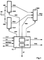
- FIG. 1 A first embodiment of the controller in accordance with the present invention is illustrated, through a block diagram, in Fig. 1.
- an address bus AB composed by a plurality of address lines and comprises:
- the control unit CU comprises, in turn, register means STR and stores therein the current operation mode, determined by the received input control signals; the information contained in the register means STR is output by the control unit through the state signal ST.
- control unit CU serves to drive all the controller operation, that as to normal operations and relative structure does not differ from the operation of the control integrated circuits already present or the market, such as the above-mentioned SN74ACT4503 device.
- the control unit will send the registers COR, ROR and MER respective selection signals SEC, SER and SEM moreover, it will have to generate at least a CAS signal and at least a RAS signal for the memory bank.
- control unit will receive at its input an enable signal CS and will output a ready signal RDY; the activation of signal CS indicates to the controller the request for accessing the memory bank, the control unit CU will answer this request through the RDY signal.
- the control unit CU can then receive a request signal REFREQ for the starting of the refresh operation.
- control unit can comprise a counter CNT for generating the refresh address REA.
- controller in accordance with the present invention can be advantageously realized through an integrated circuit by providing that at least one terminal of the integrated circuit is corrected to the register means STR.
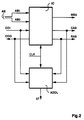
- FIG. 2 A second embodiment of the controller in accordance with the present invention is illustrated through a block diagram, in Fig. 2.
- the control integrated circuit IC can be selected from the many available on the market, for instance the above-mentioned SN74ACT4503; the input (COI) and output (COO) control signals depend on the selected integrated circuit and may comprise, e.g., a selection signal, a ready signal, a refresh operation start request signal, and so on; naturally the integrated circuit IC will receive the address bus AB and will output the memory address MEA and at least one RAS and one CAS signals.
- the additional logic ADDL will differ remarkably depending on the selected type of integrated circuit IC and in particular on the number and type of control signals COI and COO available to it; in some instances it will be necessary to provide the logic ADDL also with CAS and RAS signals generated by the integrated circuit IC; in general it will be a sequential logic but it cannot be excluded that, in particularly advantageous cases, a people skilled in the art will be able to obtain a purely combinatory realization capable of determining the current operation mode on the basis of signals fed at its input.
- Such circuit comprises:
- the decoding logic DEL selects all the four banks when the controller DRAMC operates in accordance with the second (refresh) operation mode, and selects one bank, individuated by the bank address when controller DRAMC operates in accordance with the first (access) operation mode.
- Controller DRAMC can be selected, e.g., from one of the two realizations of the present invention described previously; it generates at least one RAS signal and at least one CAS signal; naturally it will receive at its input and will output several further signals not shown in Fig. 3 and necessary for its operation.
- the decoding logic DEL receives at its input the two lines L1 and L2 and the state signal ST (having logical value "1" when a refresh operation is in progress) and outputs four bank selection signals BS1, BS2, BS3, BS4; the two lines of bus BB are entered a decoder DEC having four outputs U1, U2, U3, U4; the logical value of such outputs is provided by the following table L1/L2 U1 U2 U3 U4 0/0 1 0 0 0 0 0/1 0 1 0 1/0 0 0 1 0 1/1 0 0 0 1 1
- Outputs U1, U2, U3, U4 are then fed to the first inputs of four two-input OR-gates designated by OR1, OR2, OR3, OR4 respectively; the second inputs of gates OR1, OR2, OR3, OR4 are connected in parallel with state signal ST; the outputs of the four gates constitute the four bank signals, respectively.
- Bank selection signals BS1, BS2, BS3, BS4 could be used for directly selecting four dynamic RAM banks; dynamic RAMs are not often provided With a selection input as in the realization of Fig. 3.
- Dynamic random access memory bank BM is provided with an address input AI, a CAS-input CAI and a RAS-input RAI (active high in the realization); moreover, there is at least a data input/output not shown.
- the selection of the bank occurs automatically when inputs CAI and/or RAI are activated.
- the first input of gate CAND receives the CAS signal from The first input of gate CAND receives the CAS signal from controller DRAMC and the second input receives the corresponding bank select signal (signal BS1 in Fig. 3) and the output of gate CAND is connected with input CAI of bank BM.
- the first input of gate RAND receives the RAS signal from controller DRAMC and the second input receives the corresponding bank select signal (signal BS1 in Fig. 3) and the output of gate RAND is connected with input RAI of bank BM.
- the respective bank select signal (signal BS1 in Fig. 3) must have logical value "1".
Landscapes
- Engineering & Computer Science (AREA)
- Microelectronics & Electronic Packaging (AREA)
- Computer Hardware Design (AREA)
- Dram (AREA)
Applications Claiming Priority (2)
| Application Number | Priority Date | Filing Date | Title |
|---|---|---|---|
| IT93MI000981A IT1264443B1 (it) | 1993-05-14 | 1993-05-14 | Controllore per ram dinamiche e circuito per il controllo di una pluralita' di banchi di memoria ram dinamica |
| ITMI930981 | 1993-05-14 |
Publications (2)
| Publication Number | Publication Date |
|---|---|
| EP0631288A2 true EP0631288A2 (fr) | 1994-12-28 |
| EP0631288A3 EP0631288A3 (fr) | 1995-08-09 |
Family
ID=11366156
Family Applications (1)
| Application Number | Title | Priority Date | Filing Date |
|---|---|---|---|
| EP94107115A Ceased EP0631288A3 (fr) | 1993-05-14 | 1994-05-06 | Dispositif de commande de RAM dynamique et circuit de commande d'une pluralité de bancs de mémoires dynamiques à accès aléatoire. |
Country Status (2)
| Country | Link |
|---|---|
| EP (1) | EP0631288A3 (fr) |
| IT (1) | IT1264443B1 (fr) |
Cited By (1)
| Publication number | Priority date | Publication date | Assignee | Title |
|---|---|---|---|---|
| EP0794534A3 (fr) * | 1996-03-06 | 1999-02-03 | NOKIA TECHNOLOGY GmbH | Régénération de bancs de mémoire DRAM |
Family Cites Families (1)
| Publication number | Priority date | Publication date | Assignee | Title |
|---|---|---|---|---|
| US4542454A (en) * | 1983-03-30 | 1985-09-17 | Advanced Micro Devices, Inc. | Apparatus for controlling access to a memory |
-
1993
- 1993-05-14 IT IT93MI000981A patent/IT1264443B1/it active IP Right Grant
-
1994
- 1994-05-06 EP EP94107115A patent/EP0631288A3/fr not_active Ceased
Cited By (1)
| Publication number | Priority date | Publication date | Assignee | Title |
|---|---|---|---|---|
| EP0794534A3 (fr) * | 1996-03-06 | 1999-02-03 | NOKIA TECHNOLOGY GmbH | Régénération de bancs de mémoire DRAM |
Also Published As
| Publication number | Publication date |
|---|---|
| IT1264443B1 (it) | 1996-09-23 |
| EP0631288A3 (fr) | 1995-08-09 |
| ITMI930981A1 (it) | 1994-11-14 |
| ITMI930981A0 (it) | 1993-05-14 |
Similar Documents
| Publication | Publication Date | Title |
|---|---|---|
| US5251178A (en) | Low-power integrated circuit memory | |
| JPH0765572A (ja) | 半導体記憶装置 | |
| KR920008598A (ko) | 직접 또는 인터리브모드로 메모리를 액세스하는 메모리 컨트롤러 및 이를 구비한 데이타 처리시스템 | |
| JPH09265775A (ja) | 半導体記憶装置 | |
| US5848431A (en) | Synchronous SRAMs having multiple chip select inputs and a standby chip enable input | |
| US4763302A (en) | Alternatively addressed semiconductor memory array | |
| US6035381A (en) | Memory device including main memory storage and distinct key storage accessed using only a row address | |
| US6215719B1 (en) | Memory device having line address counter for making next line active while current line is processed | |
| EP0631288A2 (fr) | Dispositif de commande de RAM dynamique et circuit de commande d'une pluralité de bancs de mémoires dynamiques à accès aléatoire | |
| KR0136534B1 (ko) | 반도체 기억 장치 | |
| US5831906A (en) | Read/write collison-free static random access memory | |
| US6330198B1 (en) | Semiconductor storage device | |
| US6426913B1 (en) | Semiconductor memory device and layout method thereof | |
| US6560159B2 (en) | Block arrangement for semiconductor memory apparatus | |
| US7133992B2 (en) | Burst counter controller and method in a memory device operable in a 2-bit prefetch mode | |
| JPH07141864A (ja) | ダイナミック型半導体記憶装置 | |
| JPH11250660A (ja) | メモリデバイスおよび該メモリデバイスのアドレッシング方法 | |
| JPH0863969A (ja) | 半導体記憶装置 | |
| US8976617B2 (en) | Semiconductor device having plural selection lines selected based on address signal | |
| US6041015A (en) | Semiconductor type memory device having consecutive access to arbitrary memory address | |
| JP3349929B2 (ja) | メモリ制御装置 | |
| JPS6314434B2 (fr) | ||
| KR880002304Y1 (ko) | Dram의 행열 어드레스 선택회로 | |
| KR900002496Y1 (ko) | 메모리 영역 확장 회로 | |
| JPH05210580A (ja) | コンピューターシステム内のメモリをインターリーブ化するシステムおよび方法 |
Legal Events
| Date | Code | Title | Description |
|---|---|---|---|
| PUAI | Public reference made under article 153(3) epc to a published international application that has entered the european phase |
Free format text: ORIGINAL CODE: 0009012 |
|
| AK | Designated contracting states |
Kind code of ref document: A2 Designated state(s): DE ES FR GB IT NL |
|
| PUAL | Search report despatched |
Free format text: ORIGINAL CODE: 0009013 |
|
| AK | Designated contracting states |
Kind code of ref document: A3 Designated state(s): DE ES FR GB IT NL |
|
| 17P | Request for examination filed |
Effective date: 19951221 |
|
| GRAG | Despatch of communication of intention to grant |
Free format text: ORIGINAL CODE: EPIDOS AGRA |
|
| 17Q | First examination report despatched |
Effective date: 19980324 |
|
| STAA | Information on the status of an ep patent application or granted ep patent |
Free format text: STATUS: THE APPLICATION HAS BEEN REFUSED |
|
| 18R | Application refused |
Effective date: 19980913 |