EP0631297A2 - Procédé pour la croissance de silicium à basse température et dispositifs obtenus - Google Patents
Procédé pour la croissance de silicium à basse température et dispositifs obtenus Download PDFInfo
- Publication number
- EP0631297A2 EP0631297A2 EP94304322A EP94304322A EP0631297A2 EP 0631297 A2 EP0631297 A2 EP 0631297A2 EP 94304322 A EP94304322 A EP 94304322A EP 94304322 A EP94304322 A EP 94304322A EP 0631297 A2 EP0631297 A2 EP 0631297A2
- Authority
- EP
- European Patent Office
- Prior art keywords
- layer
- substrate
- silicon
- buffer layer
- glass
- Prior art date
- Legal status (The legal status is an assumption and is not a legal conclusion. Google has not performed a legal analysis and makes no representation as to the accuracy of the status listed.)
- Withdrawn
Links
Images

Classifications
-
- H—ELECTRICITY
- H10—SEMICONDUCTOR DEVICES; ELECTRIC SOLID-STATE DEVICES NOT OTHERWISE PROVIDED FOR
- H10P—GENERIC PROCESSES OR APPARATUS FOR THE MANUFACTURE OR TREATMENT OF DEVICES COVERED BY CLASS H10
- H10P14/00—Formation of materials, e.g. in the shape of layers or pillars
- H10P14/20—Formation of materials, e.g. in the shape of layers or pillars of semiconductor materials
- H10P14/29—Formation of materials, e.g. in the shape of layers or pillars of semiconductor materials characterised by the substrates
- H10P14/2901—Materials
- H10P14/2922—Materials being non-crystalline insulating materials, e.g. glass or polymers
-
- H—ELECTRICITY
- H10—SEMICONDUCTOR DEVICES; ELECTRIC SOLID-STATE DEVICES NOT OTHERWISE PROVIDED FOR
- H10P—GENERIC PROCESSES OR APPARATUS FOR THE MANUFACTURE OR TREATMENT OF DEVICES COVERED BY CLASS H10
- H10P14/00—Formation of materials, e.g. in the shape of layers or pillars
- H10P14/20—Formation of materials, e.g. in the shape of layers or pillars of semiconductor materials
- H10P14/22—Formation of materials, e.g. in the shape of layers or pillars of semiconductor materials using physical deposition, e.g. vacuum deposition or sputtering
-
- H—ELECTRICITY
- H10—SEMICONDUCTOR DEVICES; ELECTRIC SOLID-STATE DEVICES NOT OTHERWISE PROVIDED FOR
- H10P—GENERIC PROCESSES OR APPARATUS FOR THE MANUFACTURE OR TREATMENT OF DEVICES COVERED BY CLASS H10
- H10P14/00—Formation of materials, e.g. in the shape of layers or pillars
- H10P14/20—Formation of materials, e.g. in the shape of layers or pillars of semiconductor materials
- H10P14/24—Formation of materials, e.g. in the shape of layers or pillars of semiconductor materials using chemical vapour deposition [CVD]
-
- H—ELECTRICITY
- H10—SEMICONDUCTOR DEVICES; ELECTRIC SOLID-STATE DEVICES NOT OTHERWISE PROVIDED FOR
- H10P—GENERIC PROCESSES OR APPARATUS FOR THE MANUFACTURE OR TREATMENT OF DEVICES COVERED BY CLASS H10
- H10P14/00—Formation of materials, e.g. in the shape of layers or pillars
- H10P14/20—Formation of materials, e.g. in the shape of layers or pillars of semiconductor materials
- H10P14/32—Formation of materials, e.g. in the shape of layers or pillars of semiconductor materials characterised by intermediate layers between substrates and deposited layers
- H10P14/3202—Materials thereof
- H10P14/3238—Materials thereof being insulating materials
-
- H—ELECTRICITY
- H10—SEMICONDUCTOR DEVICES; ELECTRIC SOLID-STATE DEVICES NOT OTHERWISE PROVIDED FOR
- H10P—GENERIC PROCESSES OR APPARATUS FOR THE MANUFACTURE OR TREATMENT OF DEVICES COVERED BY CLASS H10
- H10P14/00—Formation of materials, e.g. in the shape of layers or pillars
- H10P14/20—Formation of materials, e.g. in the shape of layers or pillars of semiconductor materials
- H10P14/32—Formation of materials, e.g. in the shape of layers or pillars of semiconductor materials characterised by intermediate layers between substrates and deposited layers
- H10P14/3258—Crystal orientation
-
- H—ELECTRICITY
- H10—SEMICONDUCTOR DEVICES; ELECTRIC SOLID-STATE DEVICES NOT OTHERWISE PROVIDED FOR
- H10P—GENERIC PROCESSES OR APPARATUS FOR THE MANUFACTURE OR TREATMENT OF DEVICES COVERED BY CLASS H10
- H10P14/00—Formation of materials, e.g. in the shape of layers or pillars
- H10P14/20—Formation of materials, e.g. in the shape of layers or pillars of semiconductor materials
- H10P14/34—Deposited materials, e.g. layers
- H10P14/3402—Deposited materials, e.g. layers characterised by the chemical composition
- H10P14/3404—Deposited materials, e.g. layers characterised by the chemical composition being Group IVA materials
- H10P14/3411—Silicon, silicon germanium or germanium
-
- G—PHYSICS
- G02—OPTICS
- G02F—OPTICAL DEVICES OR ARRANGEMENTS FOR THE CONTROL OF LIGHT BY MODIFICATION OF THE OPTICAL PROPERTIES OF THE MEDIA OF THE ELEMENTS INVOLVED THEREIN; NON-LINEAR OPTICS; FREQUENCY-CHANGING OF LIGHT; OPTICAL LOGIC ELEMENTS; OPTICAL ANALOGUE/DIGITAL CONVERTERS
- G02F1/00—Devices or arrangements for the control of the intensity, colour, phase, polarisation or direction of light arriving from an independent light source, e.g. switching, gating or modulating; Non-linear optics
- G02F1/01—Devices or arrangements for the control of the intensity, colour, phase, polarisation or direction of light arriving from an independent light source, e.g. switching, gating or modulating; Non-linear optics for the control of the intensity, phase, polarisation or colour
- G02F1/13—Devices or arrangements for the control of the intensity, colour, phase, polarisation or direction of light arriving from an independent light source, e.g. switching, gating or modulating; Non-linear optics for the control of the intensity, phase, polarisation or colour based on liquid crystals, e.g. single liquid crystal display cells
- G02F1/133—Constructional arrangements; Operation of liquid crystal cells; Circuit arrangements
- G02F1/136—Liquid crystal cells structurally associated with a semi-conducting layer or substrate, e.g. cells forming part of an integrated circuit
- G02F1/1362—Active matrix addressed cells
- G02F1/1368—Active matrix addressed cells in which the switching element is a three-electrode device
-
- Y—GENERAL TAGGING OF NEW TECHNOLOGICAL DEVELOPMENTS; GENERAL TAGGING OF CROSS-SECTIONAL TECHNOLOGIES SPANNING OVER SEVERAL SECTIONS OF THE IPC; TECHNICAL SUBJECTS COVERED BY FORMER USPC CROSS-REFERENCE ART COLLECTIONS [XRACs] AND DIGESTS
- Y10—TECHNICAL SUBJECTS COVERED BY FORMER USPC
- Y10S—TECHNICAL SUBJECTS COVERED BY FORMER USPC CROSS-REFERENCE ART COLLECTIONS [XRACs] AND DIGESTS
- Y10S438/00—Semiconductor device manufacturing: process
- Y10S438/967—Semiconductor on specified insulator
Definitions
- the present invention relates to methods for growing at low temperature layers of epitaxial silicon. Such layers are particularly useful for making thin film transistors and lightweight flat-panel display devices.
- the AMLCD comprises an array of thin film transistors, capacitors and electrodes formed on a transparent substrate and incorporated in an LCD display. Each thin film transistor controls an electrode which, in turn, polarizes a pixel-size region of liquid crystal.
- the transistors are comprised of thin films of amorphous silicon.
- amorphous silicon lacks sufficient electron mobility to be used for drivers and registers in the display. Hence a hybrid structure combining amorphous silicon on glass and a crystalline silicon chip is required.
- Polysilicon has higher electron mobility than amorphous silicon, and if polysilicon can be substituted for amorphous silicon in AMLCD devices, the entire display --complete with drivers-- can be integrated on the substrate.
- few transparent materials can withstand the high temperatures, typically in excess of 600°C, required to grow polysilicon. Consequently efforts to make polysilicon based displays have required substrates of high temperature glass, such as fused quartz which are expensive, heavy, and fragile.
- typical thin films of polysilicon have randomly oriented grains producing random distribution of defect densities and non-uniform etching and oxidation characteristics. Accordingly, there is a need for a method for low temperature growth of silicon of enhanced electron mobility and reduced grain structure (hereafter "epitaxial silicon”) which can utilize a wider variety of substrate materials.
- a thin layer of epitaxial silicon is grown at low temperatures at or below 300°C by the steps of providing a substrate, forming an oriented dielectric buffer layer on the substrate and growing epitaxial silicon on the buffer layer.
- the substrate has a glass surface and the oriented buffer layer is cubic ZrO2.
- the buffer layer is preferably oriented by bombarding it with a directed ion beam while the buffer layer is being deposited on the substrate.
- a buffer layer of (100) cubic ZrO2 can be grown at a temperature as low as 300°C.
- the oriented cubic ZrO2 is an excellent buffer for epitaxial silicon on glass due to a good match of lattice parameters with silicon and a good match of thermal expansion coefficients with glass.
- An oriented (100) silicon epitaxial film can then be grown on the epitaxial template provided by the buffer layer at a temperature as low as 250°C.
- This low temperature process for producing epitaxial films offers multiple advantages: (1) reduced silicon interfacial defect densities and enlarged grain size permitting improved thin film transistor performance due to a lowered "off' current; (2) higher electron mobility permitting the fabrication of integrated displays; (3) lower temperature processing permitting the use of inexpensive glass substrates such as borosilicates; (4) sufficiently low temperature processing to permit the use of new lightweight substrates such as glass-coated polymeric materials (glass-coated plastics) which can substantially reduce the weight of displays and thus enhance the portability of portable computers, video telephones, and personal communicators; and (5) the use of new buffer layers such as ZrO2 which can block the diffusion of Na ions from the substrate.
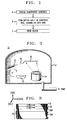
- FIG. 1 illustrates the steps for low temperature growth of polysilicon.
- the first step is to provide a suitable substrate such as a transparent body of glass or plastic.
- Preferred glasses include borosilicates such as Corning 7059.
- Preferred plastics include polyimides and polyethersulfone (PES).
- Advantageously plastic substrates are provided with a micron thick glass seed layer as by RF sputtering at low temperature.
- the next step shown in block B is to provide the substrate with a suitable buffer layer for the epitaxial growth of silicon.
- the layer should be dielectric, have lattice parameters closely matching those of silicon (preferably matching within about 5%), and have a coefficient of thermal expansion which closely matches the substrate.
- Preferred buffer layer materials include cubic ZrO2 stabilized by 8% yttrium, CeO2 ,PrO2, and Y2O3.
- the buffer layer is applied as an oriented layer by subjecting the substrate to a low energy ion bombardment at the same time the buffer layer is being applied.
- the beam is directed to maintain a velocity component in a predetermined direction parallel to the growth surface. Such a directed ion beam will preferentially remove misoriented grains and thereby promote the growth of an oriented buffer layer.
- the ion energy can be chosen below the energy level producing significant ablation of the buffer layer crystal structure.
- ZrO2 buffer layers can be grown by e-beam evaporation while bombarding a glass-surfaced substrate with a beam of argon ions preferably having energy in the range 50-200 volts. This process can achieve a buffer layer with a (100) orientation in the predetermined direction, and a mosaic spread in the plane better than 2°.
- the third step shown in block C of FIG. 1 is to grow epitaxial silicon on the buffer layer using standard processes such as sputtering or low pressure chemical vapor deposition (CVD).
- This step can be better understood by reference to FIG. 2 which schematically shows preferred apparatus for both applying a buffer layer and growing the silicon layer.
- the substrate 20 is mounted within the low pressure growth chamber 21 having a buffer source container 23 (e.g. ZrO2) using e-beam evaporation and a silicon source container 24 using sputter deposition.
- the chamber is provided with means, such as an ion gun 25, for directing a beam of ions 26 such as argon onto substrate 20.
- chamber 21 is evacuated to a low pressure of about 10 ⁇ 6Torr or lower.
- the substrate 20 is heated to a temperature of about 300°C by a heating element (not shown), and an electron beam is applied to source 23 to apply a thin buffer layer (about 500 ⁇ -5000 ⁇ thick) to the substrate and, at the same time, ion gun 25 is activated to direct a stream of argon ions at an angle of about 30° onto the growing surface.
- the buffer layer is grown with its (100) plane parallel to the major surface of the workpiece.
- the silicon source 24 will apply silicon atoms to the workpiece by sputtering with argon ions (or by low pressure CVD process). After silicon growth deposition, vacuum is broken and the epitaxial silicon coated workpiece is removed from the chamber for further processing as desired.
- Fig. 3 is a schematic cross section of a resulting device showing the substrate 20 comprising a plastic body 20A having a seed layer of glass 20B.
- the substrate is transparent to visible light.
- the glass seed layer 20B can be produced on the body by RF sputter deposition from a glass target.
- Buffer layer 30 is grown on the glass surface, and silicon layer 31 is epitaxially grown on the buffer. In particular the silicon is grown with its (100) plane parallel to the major surface of the workpiece.
- FIG. 4 illustrates a preferred device comprising a self-aligned thin film transistor 40 formed on the workpiece of FIG. 3.
- Transistor 40 uses portions of an epitaxial silicon layer 31 grown in accordance with the method of FIG. 1 to form a transistor source 31A, a channel 31B and the drain 31C.
- a gate oxide 41 is thermally grown or deposited, followed by a gate 42 of metal or polysilicon.
- the source and drain 31A and 31C are formed on layer 31 by ion implantation.
- a thick insulator 43 such as SiO2 is then deposited, and metal source and drain contacts 44 and 45 are applied through vias in the insulator 43.
- FIG. 5 which is a schematic rendering of a portion of an active matrix liquid-crystal device, shows how the device of FIG. 4 can be used to make an improved flat display.
- the AMLCD comprises a liquid crystal medium (not shown) disposed between a transparent common electrode 50 and an array of transistors 40 and local electrodes 51 (preferably pixel-size) all disposed on a common substrate 20.
- Each local electrode is switched by an associated transistor 40 interconnected to an associated storage capacitor 53.
- the transistors 40 thereby control the state of the voltage on each local electrode and, in accordance with well known principles, control the optical state of a pixel size liquid crystal region.
- the AMLCD includes a back light (not shown), a diffuser 54, polarizers 55 and, if color is desired, a grid of color filter layers 56 disposed on a transparent substrate 59. Rows of transistor gates can be interconnected via conductive gate lines 57 and columns of transistor sources can be interconnected via conductive data lines 58 for switchable control of individual pixels.
- the AMLCD of FIG. 5 is of conventional construction except that the transistors 40 are epitaxial silicon thin film transistors formed of a layer of (100) oriented epitaxial silicon (not shown in FIG. 5) grown at low temperature in accordance with the method of FIG. 1.
- the transistors are self-aligned coplanar transistors 40 formed on a glass-coated plastic substrate 20 such as are shown in FIG. 4.
- the advantages of using the process of FIG. 1 and the device of FIG. 4 in this AMLCD include enhanced transistor performance and the availability of a wider variety of substrate materials such as borosilicate glasses and even glass-coated plastics.
- a substantial reduction in weight is obtainable when the low temperature process of the invention permits the fabrication of epitaxial silicon devices on plastic substrates rather than glass.
- the AMLCD devices with plastic substrates are more shock resistant, more flexible, and less expensive.
- the new low temperature process for producing epitaxial silicon films offer multiple advantages in the fabrication of thin film silicon devices.
- Thin film transistor performance is enhanced due to a lowered "off" current by reducing the interfacial defect densities and enlarging the grain size.
- Electron mobility is increased.
- Inexpensive glass substrates such as borosilicates can be used.
- New lightweight substrates such as glass-coated plastics can be used, substantially reducing the weight and increasing the portability of displays for portable computers, television sets, video telephones, and personal communicators.
- the conventional SiO2 diffusion barrier can be replaced by a ZrO2 buffer layer which blocks effectively the diffusion of Na ions from the substrate.
Landscapes
- Thin Film Transistor (AREA)
- Physical Deposition Of Substances That Are Components Of Semiconductor Devices (AREA)
- Silicon Compounds (AREA)
- Liquid Crystal (AREA)
- Recrystallisation Techniques (AREA)
Applications Claiming Priority (2)
| Application Number | Priority Date | Filing Date | Title |
|---|---|---|---|
| US82194 | 1993-06-24 | ||
| US08/082,194 US5523587A (en) | 1993-06-24 | 1993-06-24 | Method for low temperature growth of epitaxial silicon and devices produced thereby |
Publications (2)
| Publication Number | Publication Date |
|---|---|
| EP0631297A2 true EP0631297A2 (fr) | 1994-12-28 |
| EP0631297A3 EP0631297A3 (fr) | 1997-07-09 |
Family
ID=22169638
Family Applications (1)
| Application Number | Title | Priority Date | Filing Date |
|---|---|---|---|
| EP94304322A Withdrawn EP0631297A3 (fr) | 1993-06-24 | 1994-06-15 | Procédé pour la croissance de silicium à basse température et dispositifs obtenus. |
Country Status (4)
| Country | Link |
|---|---|
| US (1) | US5523587A (fr) |
| EP (1) | EP0631297A3 (fr) |
| JP (1) | JP3096573B2 (fr) |
| CA (1) | CA2122118A1 (fr) |
Cited By (4)
| Publication number | Priority date | Publication date | Assignee | Title |
|---|---|---|---|---|
| US6103318A (en) * | 1997-06-06 | 2000-08-15 | Corning Incorporated | Method for making an optical waveguide component using a low-stress silicon photomask |
| US7601430B2 (en) * | 2006-01-31 | 2009-10-13 | Los Alamos National Security, Llc | Biaxially oriented film on flexible polymeric substrate |
| EP2671966A3 (fr) * | 2012-06-08 | 2014-03-12 | Wintek Corporation | Procédé de formation de couche de silicium polycristallin en film mince |
| EP2671965A3 (fr) * | 2012-06-08 | 2014-03-12 | Wintek Corporation | Procédé de formation de couche de silicium polycristallin en film mince et procédé de formation d'un transistor à film mince |
Families Citing this family (18)
| Publication number | Priority date | Publication date | Assignee | Title |
|---|---|---|---|---|
| US5773309A (en) * | 1994-10-14 | 1998-06-30 | The Regents Of The University Of California | Method for producing silicon thin-film transistors with enhanced forward current drive |
| GB9521855D0 (en) * | 1995-10-25 | 1996-01-03 | Philips Electronics Nv | Manufacture of electronic devices comprising thin-film circuitry |
| US5817550A (en) * | 1996-03-05 | 1998-10-06 | Regents Of The University Of California | Method for formation of thin film transistors on plastic substrates |
| US5856858A (en) * | 1997-12-01 | 1999-01-05 | The Regents Of The University Of California | Plastic substrates for active matrix liquid crystal display incapable of withstanding processing temperature of over 200° C and method of fabrication |
| US6061114A (en) * | 1998-02-23 | 2000-05-09 | International Business Machines Corporation | Alignment of liquid crystal layers |
| US5909627A (en) * | 1998-05-18 | 1999-06-01 | Philips Electronics North America Corporation | Process for production of thin layers of semiconductor material |
| US6197663B1 (en) * | 1999-12-07 | 2001-03-06 | Lucent Technologies Inc. | Process for fabricating integrated circuit devices having thin film transistors |
| US7238557B2 (en) * | 2001-11-14 | 2007-07-03 | Semiconductor Energy Laboratory Co., Ltd. | Semiconductor device and method of fabricating the same |
| US7282738B2 (en) * | 2003-07-18 | 2007-10-16 | Corning Incorporated | Fabrication of crystalline materials over substrates |
| WO2005065357A2 (fr) * | 2003-12-29 | 2005-07-21 | Translucent, Inc. | Oxydes, nitrures et phosphures des terres rares et alliages ternaires a silicium |
| US7384481B2 (en) * | 2003-12-29 | 2008-06-10 | Translucent Photonics, Inc. | Method of forming a rare-earth dielectric layer |
| KR100612868B1 (ko) * | 2004-11-08 | 2006-08-14 | 삼성전자주식회사 | 실리콘 필름 제조방법 |
| US7709859B2 (en) * | 2004-11-23 | 2010-05-04 | Cree, Inc. | Cap layers including aluminum nitride for nitride-based transistors |
| JP2006351566A (ja) * | 2005-06-13 | 2006-12-28 | Sharp Corp | 窒化物系半導体レーザ素子 |
| US8491718B2 (en) | 2008-05-28 | 2013-07-23 | Karin Chaudhari | Methods of growing heteroepitaxial single crystal or large grained semiconductor films and devices thereon |
| US10199518B2 (en) | 2008-05-28 | 2019-02-05 | Solar-Tectic Llc | Methods of growing heteroepitaxial single crystal or large grained semiconductor films and devices thereon |
| US9231094B2 (en) | 2013-05-21 | 2016-01-05 | Globalfoundries Inc. | Elemental semiconductor material contact for high electron mobility transistor |
| US9276077B2 (en) | 2013-05-21 | 2016-03-01 | Globalfoundries Inc. | Contact metallurgy for self-aligned high electron mobility transistor |
Family Cites Families (7)
| Publication number | Priority date | Publication date | Assignee | Title |
|---|---|---|---|---|
| DE3124456C2 (de) * | 1980-06-23 | 1985-04-25 | Futaba Denshi Kogyo K.K., Mobara, Chiba | Halbleiterbauelement sowie Verfahren zu dessen Herstellung |
| JPS57211267A (en) * | 1981-06-22 | 1982-12-25 | Toshiba Corp | Semiconductor device and manufacture thereof |
| JPS62189747A (ja) * | 1986-02-14 | 1987-08-19 | Sharp Corp | 半導体用絶縁基板 |
| JPH0388321A (ja) * | 1989-08-31 | 1991-04-12 | Tonen Corp | 多結晶シリコン薄膜 |
| EP0456199B1 (fr) * | 1990-05-11 | 1997-08-27 | Asahi Glass Company Ltd. | Procédé pour fabriquer un transistor à film mince comprenant un semi-conducteur polycristallin |
| US5205871A (en) * | 1990-06-01 | 1993-04-27 | The United States Of America As Represented By The Secretary Of The Navy | Monocrystalline germanium film on sapphire |
| JP3213338B2 (ja) * | 1991-05-15 | 2001-10-02 | 株式会社リコー | 薄膜半導体装置の製法 |
-
1993
- 1993-06-24 US US08/082,194 patent/US5523587A/en not_active Expired - Lifetime
-
1994
- 1994-04-25 CA CA002122118A patent/CA2122118A1/fr not_active Abandoned
- 1994-06-15 EP EP94304322A patent/EP0631297A3/fr not_active Withdrawn
- 1994-06-24 JP JP06164920A patent/JP3096573B2/ja not_active Expired - Lifetime
Cited By (5)
| Publication number | Priority date | Publication date | Assignee | Title |
|---|---|---|---|---|
| US6103318A (en) * | 1997-06-06 | 2000-08-15 | Corning Incorporated | Method for making an optical waveguide component using a low-stress silicon photomask |
| US7601430B2 (en) * | 2006-01-31 | 2009-10-13 | Los Alamos National Security, Llc | Biaxially oriented film on flexible polymeric substrate |
| EP2671966A3 (fr) * | 2012-06-08 | 2014-03-12 | Wintek Corporation | Procédé de formation de couche de silicium polycristallin en film mince |
| EP2671965A3 (fr) * | 2012-06-08 | 2014-03-12 | Wintek Corporation | Procédé de formation de couche de silicium polycristallin en film mince et procédé de formation d'un transistor à film mince |
| US8951921B2 (en) | 2012-06-08 | 2015-02-10 | Wintek Corporation | Method of forming thin film poly silicon layer and method of forming thin film transistor |
Also Published As
| Publication number | Publication date |
|---|---|
| JP3096573B2 (ja) | 2000-10-10 |
| EP0631297A3 (fr) | 1997-07-09 |
| JPH07149508A (ja) | 1995-06-13 |
| US5523587A (en) | 1996-06-04 |
| CA2122118A1 (fr) | 1994-12-25 |
Similar Documents
| Publication | Publication Date | Title |
|---|---|---|
| US5523587A (en) | Method for low temperature growth of epitaxial silicon and devices produced thereby | |
| KR100238640B1 (ko) | 반도체장치 및 그 제조방법 | |
| US6887743B2 (en) | Method of fabricating a gate dielectric layer for a thin film transistor | |
| CN100505313C (zh) | 半导体器件及其制造方法 | |
| US5466617A (en) | Manufacturing electronic devices comprising TFTs and MIMs | |
| US5153702A (en) | Thin film semiconductor device and method for fabricating the same | |
| EP1102111B1 (fr) | Dispositif d'affichage à cristal liquide avec des TFTs améliorés et son procédé de fabrication | |
| KR20020032586A (ko) | 박막 트랜지스터 및 그 제조 방법 | |
| KR20050105204A (ko) | 능동 매트릭스 디스플레이 장치용 트랜지스터 및 그 제조방법 | |
| US6596572B1 (en) | Method of fabricating a thin-film transistor having a plurality of island-like regions | |
| US6717178B2 (en) | Semiconductor devices fabricated using sputtered silicon targets | |
| JP3708150B2 (ja) | 薄膜トランジスタ基板 | |
| US6472297B1 (en) | Method of producing TFT array substrate for liquid crystal display device | |
| KR950004789B1 (ko) | 다결정실리콘의 결정성장법 | |
| JP2835580B2 (ja) | 平板型光弁駆動用半導体装置 | |
| JPS58192375A (ja) | 薄膜トランジスタの製造方法 | |
| JPH0334465A (ja) | 薄膜トランジスタおよびその製造方法並びに液晶ディスプレイ装置 | |
| Hanna et al. | Materials in Active-Matrix Liquid-Crystal Displays | |
| KR20040090302A (ko) | 박막트랜지스터 및 그 형성방법 | |
| JPH04236465A (ja) | 薄膜トランジスタおよびその製造方法 | |
| JPH0330296B2 (fr) | ||
| KR0128522B1 (ko) | 저온 다결정질 실리콘 박막 구조 및 그 제조방법, 저온 다결정질 실리콘 박막 트랜지스터 및 그 제조 방법 | |
| JP3288968B2 (ja) | 薄膜トランジスタの製造方法およびそれを用いた液晶表示装置の製造方法 | |
| JPH0336313B2 (fr) | ||
| JPH11282013A (ja) | 液晶表示装置用tftアレイとその製造方法およびそれを用いた液晶表示装置とその製造方法 |
Legal Events
| Date | Code | Title | Description |
|---|---|---|---|
| PUAI | Public reference made under article 153(3) epc to a published international application that has entered the european phase |
Free format text: ORIGINAL CODE: 0009012 |
|
| AK | Designated contracting states |
Kind code of ref document: A2 Designated state(s): DE FR GB NL |
|
| PUAL | Search report despatched |
Free format text: ORIGINAL CODE: 0009013 |
|
| AK | Designated contracting states |
Kind code of ref document: A3 Designated state(s): DE FR GB NL |
|
| STAA | Information on the status of an ep patent application or granted ep patent |
Free format text: STATUS: THE APPLICATION IS DEEMED TO BE WITHDRAWN |
|
| 18D | Application deemed to be withdrawn |
Effective date: 19980110 |