EP0631301A1 - Procédé pour la fabrication d'un dispositif de puissance à semi-conducteur pour hautes pentes de commutation - Google Patents
Procédé pour la fabrication d'un dispositif de puissance à semi-conducteur pour hautes pentes de commutation Download PDFInfo
- Publication number
- EP0631301A1 EP0631301A1 EP94109103A EP94109103A EP0631301A1 EP 0631301 A1 EP0631301 A1 EP 0631301A1 EP 94109103 A EP94109103 A EP 94109103A EP 94109103 A EP94109103 A EP 94109103A EP 0631301 A1 EP0631301 A1 EP 0631301A1
- Authority
- EP
- European Patent Office
- Prior art keywords
- zone
- polished
- semiconductor body
- conductivity type
- doped
- Prior art date
- Legal status (The legal status is an assumption and is not a legal conclusion. Google has not performed a legal analysis and makes no representation as to the accuracy of the status listed.)
- Ceased
Links
- 239000004065 semiconductor Substances 0.000 title claims abstract description 28
- 238000000034 method Methods 0.000 title claims description 12
- 238000004519 manufacturing process Methods 0.000 title claims description 4
- 238000009792 diffusion process Methods 0.000 claims 2
- 230000000903 blocking effect Effects 0.000 abstract 1
- 230000001066 destructive effect Effects 0.000 abstract 1
- 230000007704 transition Effects 0.000 description 8
- 239000000463 material Substances 0.000 description 4
- 238000011161 development Methods 0.000 description 2
- 230000018109 developmental process Effects 0.000 description 2
- 238000005530 etching Methods 0.000 description 2
- 230000001939 inductive effect Effects 0.000 description 2
- ZOXJGFHDIHLPTG-UHFFFAOYSA-N Boron Chemical compound [B] ZOXJGFHDIHLPTG-UHFFFAOYSA-N 0.000 description 1
- 229910052796 boron Inorganic materials 0.000 description 1
- 239000013078 crystal Substances 0.000 description 1
- 230000006378 damage Effects 0.000 description 1
- 230000001419 dependent effect Effects 0.000 description 1
- 239000002019 doping agent Substances 0.000 description 1
- 238000005498 polishing Methods 0.000 description 1
- 238000003672 processing method Methods 0.000 description 1
- 238000000926 separation method Methods 0.000 description 1
- 239000000126 substance Substances 0.000 description 1
- 235000012431 wafers Nutrition 0.000 description 1
Images

Classifications
-
- H—ELECTRICITY
- H10—SEMICONDUCTOR DEVICES; ELECTRIC SOLID-STATE DEVICES NOT OTHERWISE PROVIDED FOR
- H10D—INORGANIC ELECTRIC SEMICONDUCTOR DEVICES
- H10D8/00—Diodes
- H10D8/01—Manufacture or treatment
- H10D8/041—Manufacture or treatment of multilayer diodes
-
- Y—GENERAL TAGGING OF NEW TECHNOLOGICAL DEVELOPMENTS; GENERAL TAGGING OF CROSS-SECTIONAL TECHNOLOGIES SPANNING OVER SEVERAL SECTIONS OF THE IPC; TECHNICAL SUBJECTS COVERED BY FORMER USPC CROSS-REFERENCE ART COLLECTIONS [XRACs] AND DIGESTS
- Y10—TECHNICAL SUBJECTS COVERED BY FORMER USPC
- Y10S—TECHNICAL SUBJECTS COVERED BY FORMER USPC CROSS-REFERENCE ART COLLECTIONS [XRACs] AND DIGESTS
- Y10S148/00—Metal treatment
- Y10S148/126—Power FETs
-
- Y—GENERAL TAGGING OF NEW TECHNOLOGICAL DEVELOPMENTS; GENERAL TAGGING OF CROSS-SECTIONAL TECHNOLOGIES SPANNING OVER SEVERAL SECTIONS OF THE IPC; TECHNICAL SUBJECTS COVERED BY FORMER USPC CROSS-REFERENCE ART COLLECTIONS [XRACs] AND DIGESTS
- Y10—TECHNICAL SUBJECTS COVERED BY FORMER USPC
- Y10S—TECHNICAL SUBJECTS COVERED BY FORMER USPC CROSS-REFERENCE ART COLLECTIONS [XRACs] AND DIGESTS
- Y10S438/00—Semiconductor device manufacturing: process
- Y10S438/974—Substrate surface preparation
Definitions
- the invention relates to a method for producing a power semiconductor component with at least one flat surface and with a semiconductor body with at least two zones of the first or second power type.
- Such power semiconductor devices can e.g. Diodes or thyristors.
- Diodes are not only used as uncontrolled rectifiers, but are increasingly used as free-wheeling or circuit diodes in converter circuits. In such circuits, they absorb the current imposed by an inductive load in the switch-off phase. Since this current is to be quickly commutated in the interest of a high switching speed, a high voltage arises at the inductive load, which is also present at the diode. Since a high current flows here at the same time, there are high losses in the diode, which can destroy it.
- the invention is based on the object of developing a power semiconductor component of the type mentioned in such a way that the loads mentioned can be increased without the semiconductor component being destroyed.
- This object is achieved in that a semiconductor body of the first conductivity type is polished on at least one of its flat surfaces and in that the zone of the second Line type is generated from this surface.
- the invention is based on the finding that crystal disturbances are generated in these surfaces by the usual processing methods for the surface of power semiconductor components, such as grinding or lapping. If dopants are diffused into the semiconductor body starting from such a disturbed surface, an inhomogeneous pn junction is produced. These inhomogeneities are the cause of the diode overloads and failures mentioned above. It is also conceivable that they can be used in a similar manner for the destruction of thyristors with a short dimension, e.g. asymmetrical thyristors, are responsible.
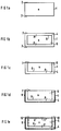
- An n-doped semiconductor body is designated by 1 in FIG. 1a. It has an upper surface 2 and a lower surface 3.
- the surface 2 is processed as usual, eg lapped and etched.
- the surface 3, however, is polished. This polishing is known from the manufacture of semiconductor wafers for integrated semiconductors. It leads to a reflective surface with an average deviation of less than 0.1 ⁇ m.
- a p-doping substance for example boron, is diffused into the semiconductor body 1 on all sides. This creates a p-doped zone 4, an n-doped zone 5 remains.
- the part of the p-doped zone 4 adjacent to the surface 2 is removed, for example by grinding, lapping or etching. This creates a surface 7.
- N-doping material is now diffused into the surface 7 after the remaining surface of the semiconductor body 1 has been provided with an oxide mask 8 (FIG. 1d).
- the edge region of the p-doped zone 4 is removed mechanically and chemically along the dashed lines 10. This creates a mesa structure. Since the heavily n-doped zone 9 was generated from the relatively strongly disturbed surface 7, the nn+ transition lying between the zones 5 and 9 is relatively inhomogeneous.
- the surface 7 can be polished like the surface 3 after grinding and etching. Then the nn+ transition between zones 5 and 9 becomes homogeneous and essentially trouble-free.
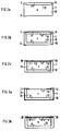
- the n-doped semiconductor body is again designated by 1.
- the upper surface 2 and the lower surface 3 are polished.
- a heavily n-doped epitaxial layer 14 is then produced on the surface 2.
- p-doping material is diffused into the semiconductor body including zone 14 on all sides. This creates a p-doped zone 16 and also zone 14 diffuses somewhat into zone 15 and p-doped layer 16.
- the part of the p-zone 16 on the side of the epitaxial layer 14 is removed. This creates a surface 17.
- the edge region of the p-doped zone 16 is removed along the dashed lines 18, so that again a mesa structure with the zone sequence n+np is created (FIG. 2c).
- the step according to FIG. 2c can be followed by two further steps instead of the separation along the dashed line 18, which are shown in FIGS. 3a and 3b.
- n-doping material can be diffused into the surface 17, so that a heavily n-doped zone 19 is formed, which adjoins the n-doped layer 14.
- the semiconductor body is provided with an oxide mask 21 on both sides and on the underside.
- the semiconductor body 1 can then be converted into a mesa structure by vertical cuts along the dashed lines 20.
- a p-doped epitaxial layer 22 (FIG. 4a) can also be produced on the polished surface 2.
- the surface 2 forms a pn junction 23 between the epitaxial zone 22 and the unchanged zone 21 of the semiconductor body 1.
- heavily n-doping material is diffused into the surface 3.
- the edge region and the top of the semiconductor body are protected by an oxide mask 24.
- the surface 3 can either be polished or lapped and etched, so that either a homogeneous, essentially undisturbed transition between zones 21 and 25 is produced or a more inhomogeneous transition.
- An inhomogeneous nn+ transition is sufficient for some applications. However, it is advantageous to create both transitions starting from a polished surface.
- diodes with a diameter of 23 mm and a reverse voltage V RM of 1700 V were commutated with a slope of 1200 A / ⁇ s. This commutation survived 90% of the diodes non-destructively.
Landscapes
- Mechanical Treatment Of Semiconductor (AREA)
- Crystals, And After-Treatments Of Crystals (AREA)
Applications Claiming Priority (2)
| Application Number | Priority Date | Filing Date | Title |
|---|---|---|---|
| DE4320560 | 1993-06-21 | ||
| DE4320560 | 1993-06-21 |
Publications (1)
| Publication Number | Publication Date |
|---|---|
| EP0631301A1 true EP0631301A1 (fr) | 1994-12-28 |
Family
ID=6490849
Family Applications (1)
| Application Number | Title | Priority Date | Filing Date |
|---|---|---|---|
| EP94109103A Ceased EP0631301A1 (fr) | 1993-06-21 | 1994-06-14 | Procédé pour la fabrication d'un dispositif de puissance à semi-conducteur pour hautes pentes de commutation |
Country Status (3)
| Country | Link |
|---|---|
| US (1) | US5472908A (fr) |
| EP (1) | EP0631301A1 (fr) |
| JP (1) | JPH0799173A (fr) |
Citations (4)
| Publication number | Priority date | Publication date | Assignee | Title |
|---|---|---|---|---|
| DE2411517A1 (de) * | 1973-03-12 | 1974-09-26 | Hitachi Ltd | Verfahren zum herstellen einer lichtempfindlichen heterogendiode |
| FR2317768A1 (fr) * | 1975-07-10 | 1977-02-04 | Silec Semi Conducteurs | Nouvelle diode et son procede de fabrication |
| EP0190935A2 (fr) * | 1985-02-08 | 1986-08-13 | Kabushiki Kaisha Toshiba | Procédé de fabrication de dispositifs semi-conducteurs comprenant un procédé de liaison |
| EP0190508A2 (fr) * | 1985-02-08 | 1986-08-13 | Kabushiki Kaisha Toshiba | Procédé pour fabriquer un dispositif à semi-conducteur composé |
Family Cites Families (7)
| Publication number | Priority date | Publication date | Assignee | Title |
|---|---|---|---|---|
| BE536122A (fr) * | 1954-03-05 | |||
| NL135876C (fr) * | 1963-06-11 | |||
| US3954534A (en) * | 1974-10-29 | 1976-05-04 | Xerox Corporation | Method of forming light emitting diode array with dome geometry |
| EP0161740B1 (fr) * | 1984-05-09 | 1991-06-12 | Kabushiki Kaisha Toshiba | Procédé pour la formation d'un substrat semi-conducteur |
| DE3815615A1 (de) * | 1988-05-07 | 1989-11-16 | Bosch Gmbh Robert | Verfahren zur herstellung einer hochsperrenden leistungsdiode |
| JPH0691263B2 (ja) * | 1988-10-19 | 1994-11-14 | 株式会社東芝 | 半導体装置の製造方法 |
| DE4133820A1 (de) * | 1991-10-12 | 1993-04-15 | Bosch Gmbh Robert | Verfahren zur herstellung von halbleiterelementen |
-
1994
- 1994-06-14 EP EP94109103A patent/EP0631301A1/fr not_active Ceased
- 1994-06-15 JP JP6156536A patent/JPH0799173A/ja active Pending
- 1994-06-21 US US08/263,376 patent/US5472908A/en not_active Expired - Lifetime
Patent Citations (4)
| Publication number | Priority date | Publication date | Assignee | Title |
|---|---|---|---|---|
| DE2411517A1 (de) * | 1973-03-12 | 1974-09-26 | Hitachi Ltd | Verfahren zum herstellen einer lichtempfindlichen heterogendiode |
| FR2317768A1 (fr) * | 1975-07-10 | 1977-02-04 | Silec Semi Conducteurs | Nouvelle diode et son procede de fabrication |
| EP0190935A2 (fr) * | 1985-02-08 | 1986-08-13 | Kabushiki Kaisha Toshiba | Procédé de fabrication de dispositifs semi-conducteurs comprenant un procédé de liaison |
| EP0190508A2 (fr) * | 1985-02-08 | 1986-08-13 | Kabushiki Kaisha Toshiba | Procédé pour fabriquer un dispositif à semi-conducteur composé |
Non-Patent Citations (1)
| Title |
|---|
| E.V. ASTROVA ET AL., ICED '88 PROCEEDINGS OF THE INTERNATIONAL CONFERENCE ON ELECTRICAL DRIVES, vol. 1, 20 September 1988 (1988-09-20), pages A1.2.1 - A1.2.4 * |
Also Published As
| Publication number | Publication date |
|---|---|
| JPH0799173A (ja) | 1995-04-11 |
| US5472908A (en) | 1995-12-05 |
Similar Documents
| Publication | Publication Date | Title |
|---|---|---|
| DE69631664T2 (de) | SiC-HALBLEITERANORDNUNG MIT EINEM PN-ÜBERGANG, DER EINEN RAND ZUR ABSORPTION DER SPANNUNG ENTHÄLT | |
| DE69331052T2 (de) | Integrierte Randstruktur für Hochspannung-Halbleiteranordnungen und dazugehöriger Herstellungsprozess | |
| DE112011103230B4 (de) | Non-Punch-Through-Bipolarleistungshalbleiterbauelement und ein Verfahren zum Herstellen eines derartigen Halbleiterbauelements | |
| DE2214935A1 (de) | Integrierte Halbleiterschaltung | |
| DE3806164C2 (fr) | ||
| DE69621088T2 (de) | Bipolartransistor und Verfahren zur Herstellung | |
| DE102017121878B4 (de) | Leistungsdiode | |
| DE69425295T2 (de) | Schutzdiode für einen Transistor | |
| DE2040911A1 (de) | Verfahren zum Herstellen eines Halbleiterbauelements | |
| DE2021691A1 (de) | Halbleiter-Bauelement | |
| DE69217427T2 (de) | Bipolartransistor mit isoliertem Gate mit einer hohen Durchbruchspannung | |
| DE4320780A1 (de) | Halbleiteranordnung und Verfahren zur Herstellung | |
| EP0071916B1 (fr) | Transistor à effet de champ MOS de puissance et procédé de sa fabrication | |
| DE3785483T2 (de) | Halbleiteranordnung mit einem Bipolartransistor und Feldeffekttransistoren. | |
| DE3823795C2 (fr) | ||
| DE69011809T2 (de) | Halbleiteranordnung und Verfahren zu ihrer Herstellung. | |
| DE69425397T2 (de) | Seriengeschaltetes Strombegrenzerbauelement | |
| EP0144876A2 (fr) | Dispositif à semi-conducteurs | |
| EP0710988A2 (fr) | Procédé pour la fabrication des dispositifs semiconducteurs controlables par effet de champ | |
| DE69210475T2 (de) | Bidirektioneller Schaltkreis zur Unterdrückung von Einschaltspannungsstössen | |
| DE69319465T2 (de) | Gate-Turn-Off-Thyristor und dessen Verwendung in Leistungwandlern | |
| DE2535864A1 (de) | Halbleiterbauelemente | |
| DE69608651T2 (de) | Hochspannung-Siliziumdiode mit optimaler Aufstellung von Silizium-Germanium Schichten | |
| DE3005367C2 (fr) | ||
| DE1934208U (de) | Halbleiterbauelement. |
Legal Events
| Date | Code | Title | Description |
|---|---|---|---|
| PUAI | Public reference made under article 153(3) epc to a published international application that has entered the european phase |
Free format text: ORIGINAL CODE: 0009012 |
|
| AK | Designated contracting states |
Kind code of ref document: A1 Designated state(s): CH DE GB LI |
|
| 17P | Request for examination filed |
Effective date: 19950404 |
|
| 17Q | First examination report despatched |
Effective date: 19950508 |
|
| APAB | Appeal dossier modified |
Free format text: ORIGINAL CODE: EPIDOS NOAPE |
|
| APAD | Appeal reference recorded |
Free format text: ORIGINAL CODE: EPIDOS REFNE |
|
| APAD | Appeal reference recorded |
Free format text: ORIGINAL CODE: EPIDOS REFNE |
|
| STAA | Information on the status of an ep patent application or granted ep patent |
Free format text: STATUS: THE APPLICATION HAS BEEN REFUSED |
|
| 18R | Application refused |
Effective date: 20020820 |
|
| APAF | Appeal reference modified |
Free format text: ORIGINAL CODE: EPIDOSCREFNE |