EP0190508A2 - Procédé pour fabriquer un dispositif à semi-conducteur composé - Google Patents
Procédé pour fabriquer un dispositif à semi-conducteur composé Download PDFInfo
- Publication number
- EP0190508A2 EP0190508A2 EP85309449A EP85309449A EP0190508A2 EP 0190508 A2 EP0190508 A2 EP 0190508A2 EP 85309449 A EP85309449 A EP 85309449A EP 85309449 A EP85309449 A EP 85309449A EP 0190508 A2 EP0190508 A2 EP 0190508A2
- Authority
- EP
- European Patent Office
- Prior art keywords
- substrates
- compound semiconductor
- mirror
- semiconductor substrates
- inp
- Prior art date
- Legal status (The legal status is an assumption and is not a legal conclusion. Google has not performed a legal analysis and makes no representation as to the accuracy of the status listed.)
- Granted
Links
Images




Classifications
-
- H—ELECTRICITY
- H10—SEMICONDUCTOR DEVICES; ELECTRIC SOLID-STATE DEVICES NOT OTHERWISE PROVIDED FOR
- H10P—GENERIC PROCESSES OR APPARATUS FOR THE MANUFACTURE OR TREATMENT OF DEVICES COVERED BY CLASS H10
- H10P70/00—Cleaning of wafers, substrates or parts of devices
- H10P70/10—Cleaning before device manufacture, i.e. Begin-Of-Line process
- H10P70/15—Cleaning before device manufacture, i.e. Begin-Of-Line process by wet cleaning only
-
- H—ELECTRICITY
- H10—SEMICONDUCTOR DEVICES; ELECTRIC SOLID-STATE DEVICES NOT OTHERWISE PROVIDED FOR
- H10P—GENERIC PROCESSES OR APPARATUS FOR THE MANUFACTURE OR TREATMENT OF DEVICES COVERED BY CLASS H10
- H10P10/00—Bonding of wafers, substrates or parts of devices
- H10P10/12—Bonding of semiconductor wafers or semiconductor substrates to semiconductor wafers or semiconductor substrates
- H10P10/128—Bonding of semiconductor wafers or semiconductor substrates to semiconductor wafers or semiconductor substrates by direct semiconductor to semiconductor bonding
-
- Y—GENERAL TAGGING OF NEW TECHNOLOGICAL DEVELOPMENTS; GENERAL TAGGING OF CROSS-SECTIONAL TECHNOLOGIES SPANNING OVER SEVERAL SECTIONS OF THE IPC; TECHNICAL SUBJECTS COVERED BY FORMER USPC CROSS-REFERENCE ART COLLECTIONS [XRACs] AND DIGESTS
- Y10—TECHNICAL SUBJECTS COVERED BY FORMER USPC
- Y10S—TECHNICAL SUBJECTS COVERED BY FORMER USPC CROSS-REFERENCE ART COLLECTIONS [XRACs] AND DIGESTS
- Y10S148/00—Metal treatment
- Y10S148/012—Bonding, e.g. electrostatic for strain gauges
-
- Y—GENERAL TAGGING OF NEW TECHNOLOGICAL DEVELOPMENTS; GENERAL TAGGING OF CROSS-SECTIONAL TECHNOLOGIES SPANNING OVER SEVERAL SECTIONS OF THE IPC; TECHNICAL SUBJECTS COVERED BY FORMER USPC CROSS-REFERENCE ART COLLECTIONS [XRACs] AND DIGESTS
- Y10—TECHNICAL SUBJECTS COVERED BY FORMER USPC
- Y10S—TECHNICAL SUBJECTS COVERED BY FORMER USPC CROSS-REFERENCE ART COLLECTIONS [XRACs] AND DIGESTS
- Y10S148/00—Metal treatment
- Y10S148/159—Strain gauges
Definitions
- the present invention relates to a method of manufacturing a semiconductor device, and, more particularly, to a method of providing a bonded structure of two compound semiconductor substrates.
- a semiconductor device using a compound semiconductor such as GaAs has recently been attracting a great deal of attention in the fields of super high speed semiconductor devices and power semiconductor devices.
- a technique for forming a junction between semiconductor layers having different impurities or conductivity types is required.
- Various types of epitaxial growth methods are known to form such a junction.
- Liquid phase epitaxy is known as a technique for forming an epitaxial layer of a considerable thickness. In accordance with liquid phase epitaxy, it is comparatively easy to increase the thickness of an epitaxial layer. However, when a GaAs semiconductor device is formed, it is difficult to form an epitaxial layer having an impurity concentration of 10 to 10 17 /cm 3 or lower. As a result, the avalanche voltage cannot be controlled because of the high impurity concentration, and a breakdown voltage of more than several tens of V cannot be obtained.
- the impurity concentration of an epitaxial layer can be controlled to as low as about 10 14 to 10 15 /cm 3.
- a junction between different types of compound semiconductors having different band gaps can be applied as a heterojunction to various semiconductor elements.
- Various epitaxial growth methods are available for forming such a heterojunction.
- the lattice constants of the semiconductor layers must basically match. Only a very, small number of combinations such as GaAs and AlGaAs can provide a good heterojunction. In many cases, crystal defects occur due to a strain resulting from lattice mismatch, or a barrier layer may undesirably form.
- Two semiconductor substrates are prepared and their surfaces to be bonded are mirror-polished.
- the smoothness and cleanliness of polished surfaces of the substrates are significant in obtaining a bonded compound semiconductor structure having good bonding strength and a junction with good electrical characteristics in accordance with the method of the present invention.
- Surfaces of the substrates can be mirror-polished by grinding and polishing using a conventional lapping machine, and, more particularly, by mechano-chemical polishing used for polishing various types of semiconductor substrates.
- the smoothness, e.g., the surface roughness of the polished surfaces of the substrates 0 is preferably less than 500 A, and more preferably less 0 than 50 A. Note that the surface roughness is given by a maximum height (Rmax) determined in accordance with JIS B-0601 (1982).
- the polished surfaces of the substrates are cleaned. Washing with water, alcohol, organic solvent or the like and drying thereafter are performed as part of a cleaning method.
- degreasing preferably with boiling trichlene
- the polished surfaces of the substrates are brought into contact with each other in a clean atmosphere of class 1 or lower.
- class 1 represents a degree of cleanliness wherein one dust particle having a particle diameter of 0.5 ⁇ m or more is present per cubic foot of atmosphere. If the_polished surfaces are brought into contact with each other long after washing and drying, the film thickness of the natural oxide film of some compound semiconductors may be too great, adversely affecting the electrical characteristics of the junction. For this reason, the two surfaces are preferably brought into contact with each other within five minutes of washing and drying.
- a bonded structure with high bonding strength can be produced.
- Annealing is preferably performed in an inert or reducing atmosphere. If annealing is performed at a temperature below 200°C, the bonding strength is weakened and electrical characteristics at the junction are poor. On the other hand, if annealing is performed at a temperature higher than the melting point of the compound semiconductor, the condition is the same as that produced in fusion bonding. Then, a thick interlayer is formed at the bonded portion, more crystal defects form, and electrical characteristics at the junction are poor. Therefore, although the adequate annealing temperature depends on the type of compound, it is usually from 300 to 600°C.
- the substrates may crack during annealing.
- the difference in thermal expansion coefficient between the compound semiconductor substrates be below 2 x 10 /°C.
- Combinations of different types of semiconductor substrates include GaAs/InP, ZnS/GaAs, InP/InSb, GaP/InP and CdS/InP. Combinations of the same types of semiconductor substrates include GaAs/GaAs and InP/InP.
- the conductivity type, the impurity concentration and the formation portion of the impurity portion are properly selected, various types of diodes and transistors can be produced.
- a mechanism of bonding the compound semiconductor substrates according to the present invention is not yet clearly known in detail.
- the natural oxide film formed on the surface of the substrate during washing and drying of the substrate and before contacting is assumed to play an important role.
- the thickness of the natural oxide ° film is confirmed to be 10 to 30 A by Lukes (Surface Sci. Vol. 30, (1972) p91).
- two kinds of semiconductor substrates are brought into contact with each other, they are supposed to be firmly bonded with each other through the H 2 0.molecules adsorbed in the natural oxide film by hydrogen bonds. It is confirmed that, if mirror-polished surfaces of semiconductor substrates are brought into contact with each other in a vacuum, the substrates can be bonded to each other.
- the bonding force does not depend only on atmospheric pressure. It is assumed that, when the temperature of the bonded semiconductor substrates is increased, dehydration condensation will occur and constituent atoms of the semiconductor substrates will be bonded to each other through oxygen. Since excessive oxygen at the bonded interface is diffused in the substrates by annealing, alignment at the interface is improved, thereby providing more stable electrical characteristics. Condensation of oxygen was not detected by actually checking a bonded interface with an X-ray microanalyzer. This is attributable to the fact that the oxygen condensed layer vanished by oxygen diffusion into the bulk, or it is so thin that it cannot be detected by an X-ray microanalyzer having a resolution of 1 to 2 ⁇ m.
- compound semiconductor substrates having given impurity concentrations and conductivity types can easily be bonded, electrically and mechanically, with each other to provide a bonded structure. Since a high temperature step for fusing the substrate is not used in bonding of the substrates, crystal defects and formation of an interlayer at the bonded interface do not occur, thereby providing a bonded structure with good electrical characteristics. It is difficult to manufacture high-speed elements, elements with a high breakdown voltage, highly efficient solar cell, or photodiodes having a sensitivity within a wide wavelength range using only the epitaxial growth method. However, in accorance with the present invention, such elements can be manufactured. According to the present invention, compound semiconductor substrates are bonded with each other at room temperature, and then annealed. Therefore, degradation of the bonded interface which is inherent in the compound semiconductor device formation process can be prevented.
- a mirror-polished Si doped (lll) n-type GaAs substrate 11 having an impurity concentration of 10 16 /cm 3 , and a mirror-polished Zn doped (111) p-type InP substrate 12 having an impurity concentration of 1018/cm3 were prepared.
- the substrates 11 and 12 were degreased in boiling trichlene. Then, substrate 11 was immersed in concentrated boiling hydrochloric acid for two minutes, washed with water and dried by a spinner.
- the bonded substrate structure was cut into a square with 3 mm sides, using a diamond blade.
- An AuBe electrode 14 was deposited on substrate 12 as shown in Fig. 1C.
- an AuGe alloy piece was placed on substrate 11 and heated at 500°C for 30 minutes to provide AuGe electrode 13.
- substrates 21 and 22 were brought into contact and bonded with each other in a clean room of class 1, as shown in Fig. 2B.
- the resultant bonded structure was annealed in a hydrogen furnace at a temperature of 450°C for one hour to provide a firmly bonded structure.
- an AuGe alloy was deposited on substrate 21, and then an AuZn alloy was deposited on substrate 22, of the resultant bonded structure, and the structure was annealed at 400°C for one hour to provide ohmic electrodes 23 and 24.
- the diode obtained was confirmed, by curve tracer, to exhibit good diode characteristics.
- the diode exhibited a forward direction temperature characteristic substantially coincident with a predicted value.
- mirror-polished n-type InP substrate 31 having an impurity concentration of 10 /cm and a mirror-polished p-type InSb substrate 32 having an impurity concentration of 10 18 /cm 3 were prepared.
- Substrates 31 and 32 were degreased by treatment with boiling trichlene and replacement with ethanol. Thereafter, the surface of substrate 31 was cleaned in accordance with the same steps as in Example 2.
- Substrate 32 was immersed in concentrated phosphoric acid for one minute, washed with water and dried by spinner.
- the mirror-polished surfaces of substrates 31 and 32 were brought into contact with each other in a clean room of class 1, as shown in Fig. 3B, and then annealed in a hydrogen furnace at a temperature of 400°C for one hour.
- AuGe alloy lattice-shaped electrode 33 was formed on substrate 31, and then AuZn alloy electrode 34 was formed on the entire surface of substrate 33 of the resultant bonded structure, thereby completing the formation of a photodiode.
- the obtained photodiode was cooled by liquid nitrogen and its photovoltaic characteristic was measured. As a result, a photovoltaic effect was observed in a light with a wavelength of up to about 6 ⁇ m.
- conductive substrates of different materials having different conductivity types were used to manufacture a photodiode.
- a static induction transistor was manufactured using substrates of the same type.
- mirror-polished n -type GaAs substrate 41 having an impurity concentration of 10 14 /cm 3 and mirror-polished n-type GaAs substrate 42 having an impurity concentration of 10 18 /cm 3 were prepared.
- the substrates 41 and 42 were degreased in boiling trichlene, boiled in concentrated hydrochloric acid for two minutes, washed with water and dried by a spinner.
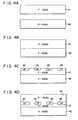
- the mirror-polished surfaces of substrates 41 and 42 were brought into contact with each other in a clean room of class 1, as shown in Fig. 4B, and annealed in a hydrogen furnace at a temperature of 500°C for one hour, thereby providing a firmly bonded structure.
- Substrate 41 of the bonded structure was polished to a thickness of 60 ⁇ m. Be was ion-implanted into substrate 41 to form p-type buried gate layer 43 having an impurity concentration of about 1 x 10 /cm , as shown in Fig. 4C.
- mirror-polished n -type GaAs substrate 44 was bonded to a surface of the layer 43 of the bonded structure. Bonding together with a pretreatment of the substrate before bonding was performed under conditions similar to those in the first bonding step. The obtained structure was annealed in a temperature (800°C for 30 minutes) sufficient to activate the previously ion-implanted Be.
- the substrate 44 was polished to a thickness of about 10 ⁇ m.
- An n-type GaAs layer 45 having an impurity concentration of about 1 x 10 18 /cm 3 and a thickness of about 0.5 ⁇ m was epitaxially formed on the substrate 44.
- mesa-etching was performed in accordance with dry etching to expose layer 43, and an AuGe alloy was deposited on the upper and lower surfaces of the structure.
- the obtained structure was annealed at a temperature of 400°C in an inert gas, thus forming drain electrode 48, source electrode 46 and gate electrode 47.
- the obtained static induction transistor exhibited a breakdown voltage of more than 600 V.
- the bonded interfaces were annealed after bonding so that the interface of GaAs was not degraded by annealing. Therefore, degradation in electrical characteristics such as decreased breakdown voltage and increased forward voltage drop were not observed.
- mirror-polished Sn doped n-type InP substrate 51 having an impurity concentration of 2 x 10 18 /cm 3 and mirror-polished Zn doped p-type InP substrate 52 having an impurity concentration of 5 x 10 18 /cm 3 were prepared. Both substrates 51 and 52 have a crystal orientation (100), a diameter of 2 inches and a thickness of 300 pm. Substrates 51 and 52 were degreased in boiling trichlene which was then substituted with ethanol.
- the obtained pn junction diode was cut to a pellet having 3 mm sides, and V-I characteristics thereof were confirmed, by curve tracer, to exhibit good diode characteristics having a high breakdown voltage.
Landscapes
- Recrystallisation Techniques (AREA)
- Junction Field-Effect Transistors (AREA)
Applications Claiming Priority (2)
| Application Number | Priority Date | Filing Date | Title |
|---|---|---|---|
| JP22932/85 | 1985-02-08 | ||
| JP60022932A JPH0770474B2 (ja) | 1985-02-08 | 1985-02-08 | 化合物半導体装置の製造方法 |
Publications (3)
| Publication Number | Publication Date |
|---|---|
| EP0190508A2 true EP0190508A2 (fr) | 1986-08-13 |
| EP0190508A3 EP0190508A3 (en) | 1988-03-02 |
| EP0190508B1 EP0190508B1 (fr) | 1991-08-28 |
Family
ID=12096402
Family Applications (1)
| Application Number | Title | Priority Date | Filing Date |
|---|---|---|---|
| EP85309449A Expired - Lifetime EP0190508B1 (fr) | 1985-02-08 | 1985-12-23 | Procédé pour fabriquer un dispositif à semi-conducteur composé |
Country Status (4)
| Country | Link |
|---|---|
| US (1) | US4738935A (fr) |
| EP (1) | EP0190508B1 (fr) |
| JP (1) | JPH0770474B2 (fr) |
| DE (1) | DE3583934D1 (fr) |
Cited By (12)
| Publication number | Priority date | Publication date | Assignee | Title |
|---|---|---|---|---|
| EP0300433A3 (fr) * | 1987-07-24 | 1989-09-13 | Kabushiki Kaisha Toshiba | Procédé pour fabriquer un corps semi-conducteur composé |
| GB2228909A (en) * | 1989-01-14 | 1990-09-12 | Clayton Edward Sampson | Roller conveyor drive and drive shaft |
| EP0425037A3 (en) * | 1989-10-23 | 1991-09-11 | Philips Electronic And Associated Industries Limited | A method of manufacturing a semiconductor device |
| US5196375A (en) * | 1987-07-24 | 1993-03-23 | Kabushiki Kaisha Toshiba | Method for manufacturing bonded semiconductor body |
| EP0631301A1 (fr) * | 1993-06-21 | 1994-12-28 | eupec Europäische Gesellschaft für Leistungshalbleiter mbH & Co. KG | Procédé pour la fabrication d'un dispositif de puissance à semi-conducteur pour hautes pentes de commutation |
| WO1996013060A1 (fr) * | 1994-10-24 | 1996-05-02 | Daimler-Benz Aktiengesellschaft | Procede de liaison directe de corps plans et objets fabriques selon ledit procede a partir de ces corps plans |
| EP0698926A3 (fr) * | 1994-08-26 | 1998-04-15 | Ngk Insulators, Ltd. | Thyristor à induction statique normalement non-conducteur et son procédé de fabrication |
| EP0663698B1 (fr) * | 1993-07-28 | 1999-09-29 | Ngk Insulators, Ltd. | Dispositf a semi-conducteurs et sa fabrication |
| US6163460A (en) * | 1997-10-11 | 2000-12-19 | Temic Telefunken Microelectronic Gmbh | Housing for electronic assemblies including board-mounted components and separate discrete components |
| US6848316B2 (en) | 2002-05-08 | 2005-02-01 | Rosemount Inc. | Pressure sensor assembly |
| US7364982B2 (en) | 1999-06-09 | 2008-04-29 | Kabushiki Kaisha Toshiba | Process for preparing a bonding type semiconductor substrate |
| EP2423356A4 (fr) * | 2009-04-20 | 2014-06-11 | Sumitomo Electric Industries | Procédé de production de substrat de phosphure d'indium, procédé de production de tranche épitaxiale, substrat de phosphure d'indium et tranche épitaxiale |
Families Citing this family (46)
| Publication number | Priority date | Publication date | Assignee | Title |
|---|---|---|---|---|
| JPS61191071A (ja) * | 1985-02-20 | 1986-08-25 | Toshiba Corp | 伝導度変調型半導体装置及びその製造方法 |
| JP2579979B2 (ja) * | 1987-02-26 | 1997-02-12 | 株式会社東芝 | 半導体素子の製造方法 |
| JPH07111940B2 (ja) * | 1987-09-11 | 1995-11-29 | 日産自動車株式会社 | 半導体基板の接合方法 |
| JP2788269B2 (ja) * | 1988-02-08 | 1998-08-20 | 株式会社東芝 | 半導体装置およびその製造方法 |
| US5164813A (en) * | 1988-06-24 | 1992-11-17 | Unitrode Corporation | New diode structure |
| US5004705A (en) * | 1989-01-06 | 1991-04-02 | Unitrode Corporation | Inverted epitaxial process |
| US5416354A (en) * | 1989-01-06 | 1995-05-16 | Unitrode Corporation | Inverted epitaxial process semiconductor devices |
| JPH0355822A (ja) * | 1989-07-25 | 1991-03-11 | Shin Etsu Handotai Co Ltd | 半導体素子形成用基板の製造方法 |
| US5213993A (en) * | 1989-09-13 | 1993-05-25 | Kabushiki Kaisha Tobisha | Method of manufacturing semiconductor substrate dielectric isolating structure |
| US5266135A (en) * | 1990-02-07 | 1993-11-30 | Harris Corporation | Wafer bonding process employing liquid oxidant |
| NL9000972A (nl) * | 1990-04-24 | 1991-11-18 | Philips Nv | Werkwijze voor het vervaardigen van een silicium lichaam met een n-type toplaag en een daaraan grenzende, hoger gedoteerde n-type basislaag. |
| JP2574612B2 (ja) * | 1992-10-13 | 1997-01-22 | 松下電器産業株式会社 | 電子音響集積回路およびその製造方法 |
| JP2976704B2 (ja) * | 1992-07-01 | 1999-11-10 | 松下電器産業株式会社 | 水晶振動子とその製造方法 |
| JP3164891B2 (ja) * | 1992-06-23 | 2001-05-14 | 松下電器産業株式会社 | 水晶振動子とその製造方法 |
| JP3164893B2 (ja) * | 1992-07-03 | 2001-05-14 | 松下電器産業株式会社 | 水晶振動子とその製造方法 |
| JP3164890B2 (ja) * | 1992-06-23 | 2001-05-14 | 松下電器産業株式会社 | 水晶振動子とその製造方法 |
| JP2973560B2 (ja) * | 1991-04-22 | 1999-11-08 | 松下電器産業株式会社 | 水晶振動子の加工方法 |
| US5183769A (en) * | 1991-05-06 | 1993-02-02 | Motorola, Inc. | Vertical current flow semiconductor device utilizing wafer bonding |
| US5207864A (en) * | 1991-12-30 | 1993-05-04 | Bell Communications Research | Low-temperature fusion of dissimilar semiconductors |
| US6909146B1 (en) | 1992-02-12 | 2005-06-21 | Intersil Corporation | Bonded wafer with metal silicidation |
| JP2689057B2 (ja) * | 1992-09-16 | 1997-12-10 | 本田技研工業株式会社 | 静電誘導型半導体装置 |
| US5380669A (en) * | 1993-02-08 | 1995-01-10 | Santa Barbara Research Center | Method of fabricating a two-color detector using LPE crystal growth |
| TW289837B (fr) * | 1994-01-18 | 1996-11-01 | Hwelett Packard Co | |
| US6484585B1 (en) | 1995-02-28 | 2002-11-26 | Rosemount Inc. | Pressure sensor for a pressure transmitter |
| JPH09246202A (ja) * | 1996-03-07 | 1997-09-19 | Shin Etsu Handotai Co Ltd | 熱処理方法および半導体単結晶基板 |
| US6153166A (en) * | 1997-06-27 | 2000-11-28 | Nippon Pillar Packing Co., Ltd. | Single crystal SIC and a method of producing the same |
| US20010042866A1 (en) * | 1999-02-05 | 2001-11-22 | Carrie Carter Coman | Inxalygazn optical emitters fabricated via substrate removal |
| JP4635079B2 (ja) * | 1999-06-09 | 2011-02-16 | 株式会社東芝 | 半導体発光素子の製造方法 |
| US6520020B1 (en) | 2000-01-06 | 2003-02-18 | Rosemount Inc. | Method and apparatus for a direct bonded isolated pressure sensor |
| US6505516B1 (en) | 2000-01-06 | 2003-01-14 | Rosemount Inc. | Capacitive pressure sensing with moving dielectric |
| AU2629901A (en) | 2000-01-06 | 2001-07-16 | Rosemount Inc. | Grain growth of electrical interconnection for microelectromechanical systems (mems) |
| US6508129B1 (en) | 2000-01-06 | 2003-01-21 | Rosemount Inc. | Pressure sensor capsule with improved isolation |
| US6561038B2 (en) | 2000-01-06 | 2003-05-13 | Rosemount Inc. | Sensor with fluid isolation barrier |
| US6525335B1 (en) | 2000-11-06 | 2003-02-25 | Lumileds Lighting, U.S., Llc | Light emitting semiconductor devices including wafer bonded heterostructures |
| JP2002185080A (ja) | 2000-12-15 | 2002-06-28 | Fujitsu Ltd | 半導体装置及びその製造方法 |
| US6727524B2 (en) * | 2002-03-22 | 2004-04-27 | Kulite Semiconductor Products, Inc. | P-n junction structure |
| JP4250576B2 (ja) * | 2004-08-24 | 2009-04-08 | 株式会社東芝 | 半導体発光素子 |
| US7806988B2 (en) * | 2004-09-28 | 2010-10-05 | Micron Technology, Inc. | Method to address carbon incorporation in an interpoly oxide |
| JP4996828B2 (ja) * | 2005-03-23 | 2012-08-08 | 本田技研工業株式会社 | 接合型半導体装置の製造方法 |
| TWI293474B (en) * | 2005-06-16 | 2008-02-11 | Advanced Semiconductor Eng | A wafer dicting process for optical electronic packing |
| JP2010045156A (ja) * | 2008-08-12 | 2010-02-25 | Toshiba Corp | 半導体装置の製造方法 |
| DE102013002637B4 (de) | 2013-02-15 | 2026-05-07 | Freiberger Compound Materials Gmbh | Verfahren zur Herstellung eines Galliumarsenidsubstrats, Galliumarsenidsubstrat und Verwendung desselben |
| DE102016013540A1 (de) * | 2016-11-14 | 2018-05-17 | 3 - 5 Power Electronics GmbH | lll-V-Halbleiterdiode |
| CN108807284B (zh) * | 2017-04-28 | 2020-06-26 | 环球晶圆股份有限公司 | 一种外延接合基板及其制造方法 |
| DE102018000395A1 (de) | 2018-01-18 | 2019-07-18 | 3-5 Power Electronics GmbH | Stapelförmige lll-V-Halbleiterdiode |
| JP7783738B2 (ja) * | 2021-12-21 | 2025-12-10 | 株式会社東芝 | 量子カスケード素子 |
Family Cites Families (8)
| Publication number | Priority date | Publication date | Assignee | Title |
|---|---|---|---|---|
| NL281360A (fr) * | 1961-07-26 | 1900-01-01 | ||
| US3351502A (en) * | 1964-10-19 | 1967-11-07 | Massachusetts Inst Technology | Method of producing interface-alloy epitaxial heterojunctions |
| JPS4926455A (fr) * | 1972-07-11 | 1974-03-08 | ||
| DE2926741C2 (de) * | 1979-07-03 | 1982-09-09 | Licentia Patent-Verwaltungs-Gmbh, 6000 Frankfurt | Feldeffekt-Transistor und Verfahren zu seiner Herstellung |
| DE2926785C2 (de) * | 1979-07-03 | 1985-12-12 | HIGRATHERM electric GmbH, 7100 Heilbronn | Bipolarer Transistor und Verfahren zu seiner Herstellung |
| JPS5696834A (en) * | 1979-12-28 | 1981-08-05 | Mitsubishi Monsanto Chem Co | Compound semiconductor epitaxial wafer and manufacture thereof |
| JPS6051700A (ja) * | 1983-08-31 | 1985-03-23 | Toshiba Corp | シリコン結晶体の接合方法 |
| EP0161740B1 (fr) * | 1984-05-09 | 1991-06-12 | Kabushiki Kaisha Toshiba | Procédé pour la formation d'un substrat semi-conducteur |
-
1985
- 1985-02-08 JP JP60022932A patent/JPH0770474B2/ja not_active Expired - Lifetime
- 1985-12-16 US US06/809,193 patent/US4738935A/en not_active Expired - Lifetime
- 1985-12-23 DE DE8585309449T patent/DE3583934D1/de not_active Expired - Lifetime
- 1985-12-23 EP EP85309449A patent/EP0190508B1/fr not_active Expired - Lifetime
Cited By (20)
| Publication number | Priority date | Publication date | Assignee | Title |
|---|---|---|---|---|
| EP0300433A3 (fr) * | 1987-07-24 | 1989-09-13 | Kabushiki Kaisha Toshiba | Procédé pour fabriquer un corps semi-conducteur composé |
| US5196375A (en) * | 1987-07-24 | 1993-03-23 | Kabushiki Kaisha Toshiba | Method for manufacturing bonded semiconductor body |
| GB2228909A (en) * | 1989-01-14 | 1990-09-12 | Clayton Edward Sampson | Roller conveyor drive and drive shaft |
| GB2228909B (en) * | 1989-01-14 | 1992-06-10 | Clayton Edward Sampson | Roller conveyor systems |
| EP0425037A3 (en) * | 1989-10-23 | 1991-09-11 | Philips Electronic And Associated Industries Limited | A method of manufacturing a semiconductor device |
| US5089431A (en) * | 1989-10-23 | 1992-02-18 | U.S. Philips Corporation | Method of manufacturing a semiconductor device including a static induction transistor |
| EP0631301A1 (fr) * | 1993-06-21 | 1994-12-28 | eupec Europäische Gesellschaft für Leistungshalbleiter mbH & Co. KG | Procédé pour la fabrication d'un dispositif de puissance à semi-conducteur pour hautes pentes de commutation |
| US5472908A (en) * | 1993-06-21 | 1995-12-05 | Eupec Europaeische Gesellsch. F. Leitsungshalbleiter Mbh & Co. Kg | Method for manufacturing a power semiconductor component for high speed current switching |
| EP0663698B1 (fr) * | 1993-07-28 | 1999-09-29 | Ngk Insulators, Ltd. | Dispositf a semi-conducteurs et sa fabrication |
| US5847417A (en) * | 1994-08-26 | 1998-12-08 | Ngk Insulators, Ltd. | Semiconductor device and method of manufacturing same |
| EP0698926A3 (fr) * | 1994-08-26 | 1998-04-15 | Ngk Insulators, Ltd. | Thyristor à induction statique normalement non-conducteur et son procédé de fabrication |
| EP0994514A1 (fr) * | 1994-08-26 | 2000-04-19 | Ngk Insulators, Ltd. | Procédé de fabrication d'un dispositif semiconducteur en joignant deux substrats |
| US6159776A (en) * | 1994-08-26 | 2000-12-12 | Ngk Insulators, Ltd. | Method for manufacturing semiconductor device |
| WO1996013060A1 (fr) * | 1994-10-24 | 1996-05-02 | Daimler-Benz Aktiengesellschaft | Procede de liaison directe de corps plans et objets fabriques selon ledit procede a partir de ces corps plans |
| US6163460A (en) * | 1997-10-11 | 2000-12-19 | Temic Telefunken Microelectronic Gmbh | Housing for electronic assemblies including board-mounted components and separate discrete components |
| US7364982B2 (en) | 1999-06-09 | 2008-04-29 | Kabushiki Kaisha Toshiba | Process for preparing a bonding type semiconductor substrate |
| EP1065734B1 (fr) * | 1999-06-09 | 2009-05-13 | Kabushiki Kaisha Toshiba | Substrat semi-conducteur du type soudage, élément électroluminescent semi-conducteur et méthode de fabrication |
| US8829488B2 (en) | 1999-06-09 | 2014-09-09 | Kabushiki Kaisha Toshiba | Process for preparing a bonding type semiconductor substrate |
| US6848316B2 (en) | 2002-05-08 | 2005-02-01 | Rosemount Inc. | Pressure sensor assembly |
| EP2423356A4 (fr) * | 2009-04-20 | 2014-06-11 | Sumitomo Electric Industries | Procédé de production de substrat de phosphure d'indium, procédé de production de tranche épitaxiale, substrat de phosphure d'indium et tranche épitaxiale |
Also Published As
| Publication number | Publication date |
|---|---|
| DE3583934D1 (de) | 1991-10-02 |
| JPS61183915A (ja) | 1986-08-16 |
| EP0190508B1 (fr) | 1991-08-28 |
| US4738935A (en) | 1988-04-19 |
| EP0190508A3 (en) | 1988-03-02 |
| JPH0770474B2 (ja) | 1995-07-31 |
Similar Documents
| Publication | Publication Date | Title |
|---|---|---|
| US4738935A (en) | Method of manufacturing compound semiconductor apparatus | |
| US7141834B2 (en) | Method of using a germanium layer transfer to Si for photovoltaic applications and heterostructure made thereby | |
| US7023010B2 (en) | Si/C superlattice useful for semiconductor devices | |
| US7427773B2 (en) | Layer transfer of low defect SiGe using an etch-back process | |
| EP0727830B1 (fr) | Liaison des couches de diode émittrice de lumière | |
| EP0190935B1 (fr) | Procédé de fabrication de dispositifs semi-conducteurs comprenant un procédé de liaison | |
| US4947218A (en) | P-N junction diodes in silicon carbide | |
| EP0485115B1 (fr) | Procédé de fabrication d'une matrice de détecteurs opto-électroniques | |
| US3647581A (en) | Manufacture of semiconductor devices | |
| JPS61292934A (ja) | 半導体素子の製造方法 | |
| Imthurn et al. | Bonded silicon‐on‐sapphire wafers and devices | |
| Chu et al. | Electrical properties of CdS/CdTe heterojunctions | |
| JP2009539255A (ja) | 薄膜光起電構造および製造 | |
| EP0190934B1 (fr) | Procédé pour fabriquer un thyristor | |
| EP0374001B1 (fr) | Procédé de durcissement vis-à-vis des rayonnements ionisants de composants électroniques actifs, et composants durcis de grandes dimensions | |
| US4004342A (en) | Fabrication of ion implanted P-N junction devices | |
| US20030000454A1 (en) | Passivation of HgCdTe junction diode by annealing in Cd/Hg atmosphere | |
| JP3313344B2 (ja) | SiC/Siヘテロ構造半導体スイッチ及びその製造方法 | |
| Katayama et al. | An MOS field‐effect transistor fabricated on a molecular‐beam epitaxial silicon layer | |
| Shin et al. | HgCdTe photodiodes formed by double‐layer liquid phase epitaxial growth | |
| JPH0770477B2 (ja) | 半導体装置の製造方法 | |
| JPS61182217A (ja) | ウエハ接着方法 | |
| Lee et al. | Rapid thermal annealing of Be+‐implanted In0. 52Al0. 48As | |
| Ludemann et al. | Dry processing of mc-silicon thin-film solar cells on foreign substrates leading to 11% efficiency | |
| JPH04229664A (ja) | 光起電力装置及びその製造方法 |
Legal Events
| Date | Code | Title | Description |
|---|---|---|---|
| PUAI | Public reference made under article 153(3) epc to a published international application that has entered the european phase |
Free format text: ORIGINAL CODE: 0009012 |
|
| AK | Designated contracting states |
Kind code of ref document: A2 Designated state(s): DE FR GB |
|
| 17P | Request for examination filed |
Effective date: 19861002 |
|
| PUAL | Search report despatched |
Free format text: ORIGINAL CODE: 0009013 |
|
| AK | Designated contracting states |
Kind code of ref document: A3 Designated state(s): DE FR GB |
|
| 17Q | First examination report despatched |
Effective date: 19900129 |
|
| GRAA | (expected) grant |
Free format text: ORIGINAL CODE: 0009210 |
|
| AK | Designated contracting states |
Kind code of ref document: B1 Designated state(s): DE FR GB |
|
| REF | Corresponds to: |
Ref document number: 3583934 Country of ref document: DE Date of ref document: 19911002 |
|
| ET | Fr: translation filed | ||
| PLBE | No opposition filed within time limit |
Free format text: ORIGINAL CODE: 0009261 |
|
| STAA | Information on the status of an ep patent application or granted ep patent |
Free format text: STATUS: NO OPPOSITION FILED WITHIN TIME LIMIT |
|
| 26N | No opposition filed | ||
| PGFP | Annual fee paid to national office [announced via postgrant information from national office to epo] |
Ref country code: FR Payment date: 19971209 Year of fee payment: 13 |
|
| PGFP | Annual fee paid to national office [announced via postgrant information from national office to epo] |
Ref country code: DE Payment date: 19971230 Year of fee payment: 13 |
|
| REG | Reference to a national code |
Ref country code: GB Ref legal event code: 746 Effective date: 19980929 |
|
| PG25 | Lapsed in a contracting state [announced via postgrant information from national office to epo] |
Ref country code: FR Free format text: LAPSE BECAUSE OF NON-PAYMENT OF DUE FEES Effective date: 19990831 |
|
| REG | Reference to a national code |
Ref country code: FR Ref legal event code: ST |
|
| PG25 | Lapsed in a contracting state [announced via postgrant information from national office to epo] |
Ref country code: DE Free format text: LAPSE BECAUSE OF NON-PAYMENT OF DUE FEES Effective date: 19991001 |
|
| REG | Reference to a national code |
Ref country code: GB Ref legal event code: IF02 |
|
| PGFP | Annual fee paid to national office [announced via postgrant information from national office to epo] |
Ref country code: GB Payment date: 20041222 Year of fee payment: 20 |
|
| PG25 | Lapsed in a contracting state [announced via postgrant information from national office to epo] |
Ref country code: GB Free format text: LAPSE BECAUSE OF EXPIRATION OF PROTECTION Effective date: 20051222 |
|
| REG | Reference to a national code |
Ref country code: GB Ref legal event code: PE20 |