EP0633611B1 - Halbleiteranordnung mit einer Bipolarfeldeffektanordnung mit isoliertem Gate - Google Patents
Halbleiteranordnung mit einer Bipolarfeldeffektanordnung mit isoliertem Gate Download PDFInfo
- Publication number
- EP0633611B1 EP0633611B1 EP94201890A EP94201890A EP0633611B1 EP 0633611 B1 EP0633611 B1 EP 0633611B1 EP 94201890 A EP94201890 A EP 94201890A EP 94201890 A EP94201890 A EP 94201890A EP 0633611 B1 EP0633611 B1 EP 0633611B1
- Authority
- EP
- European Patent Office
- Prior art keywords
- region
- subsidiary
- conductivity type
- channel
- regions
- Prior art date
- Legal status (The legal status is an assumption and is not a legal conclusion. Google has not performed a legal analysis and makes no representation as to the accuracy of the status listed.)
- Expired - Lifetime
Links
- 239000004065 semiconductor Substances 0.000 title claims description 55
- 230000005669 field effect Effects 0.000 title claims description 23
- 230000009471 action Effects 0.000 claims description 35
- 239000002800 charge carrier Substances 0.000 claims description 27
- 238000002347 injection Methods 0.000 claims description 17
- 239000007924 injection Substances 0.000 claims description 17
- 230000000977 initiatory effect Effects 0.000 claims description 12
- 108091006146 Channels Proteins 0.000 description 119
- 239000010410 layer Substances 0.000 description 21
- 150000002500 ions Chemical class 0.000 description 13
- 230000000903 blocking effect Effects 0.000 description 10
- 239000000969 carrier Substances 0.000 description 9
- 238000005516 engineering process Methods 0.000 description 8
- 238000002513 implantation Methods 0.000 description 7
- 238000000034 method Methods 0.000 description 7
- 239000000758 substrate Substances 0.000 description 7
- 230000008901 benefit Effects 0.000 description 6
- 239000002019 doping agent Substances 0.000 description 6
- 239000012535 impurity Substances 0.000 description 6
- 210000004027 cell Anatomy 0.000 description 4
- 238000009826 distribution Methods 0.000 description 4
- 238000007667 floating Methods 0.000 description 4
- 230000003071 parasitic effect Effects 0.000 description 4
- 238000005094 computer simulation Methods 0.000 description 3
- 238000009792 diffusion process Methods 0.000 description 3
- 238000005530 etching Methods 0.000 description 3
- 230000000873 masking effect Effects 0.000 description 3
- 239000000463 material Substances 0.000 description 3
- 238000001465 metallisation Methods 0.000 description 3
- 230000004048 modification Effects 0.000 description 3
- 238000012986 modification Methods 0.000 description 3
- 238000012856 packing Methods 0.000 description 3
- 241001354791 Baliga Species 0.000 description 2
- XUIMIQQOPSSXEZ-UHFFFAOYSA-N Silicon Chemical compound [Si] XUIMIQQOPSSXEZ-UHFFFAOYSA-N 0.000 description 2
- 230000015572 biosynthetic process Effects 0.000 description 2
- -1 boron ions Chemical class 0.000 description 2
- 230000007423 decrease Effects 0.000 description 2
- 238000002955 isolation Methods 0.000 description 2
- 238000004519 manufacturing process Methods 0.000 description 2
- 230000007246 mechanism Effects 0.000 description 2
- 229910052710 silicon Inorganic materials 0.000 description 2
- 239000010703 silicon Substances 0.000 description 2
- 239000002344 surface layer Substances 0.000 description 2
- XAGFODPZIPBFFR-UHFFFAOYSA-N aluminium Chemical compound [Al] XAGFODPZIPBFFR-UHFFFAOYSA-N 0.000 description 1
- 229910052782 aluminium Inorganic materials 0.000 description 1
- 239000004411 aluminium Substances 0.000 description 1
- 229910052785 arsenic Inorganic materials 0.000 description 1
- RQNWIZPPADIBDY-UHFFFAOYSA-N arsenic atom Chemical compound [As] RQNWIZPPADIBDY-UHFFFAOYSA-N 0.000 description 1
- 230000004888 barrier function Effects 0.000 description 1
- 229910052796 boron Inorganic materials 0.000 description 1
- 230000015556 catabolic process Effects 0.000 description 1
- 230000001413 cellular effect Effects 0.000 description 1
- 210000003850 cellular structure Anatomy 0.000 description 1
- 239000004020 conductor Substances 0.000 description 1
- 238000010276 construction Methods 0.000 description 1
- 238000007796 conventional method Methods 0.000 description 1
- 238000000151 deposition Methods 0.000 description 1
- 230000008021 deposition Effects 0.000 description 1
- 230000000694 effects Effects 0.000 description 1
- 238000000605 extraction Methods 0.000 description 1
- 239000012212 insulator Substances 0.000 description 1
- 238000005468 ion implantation Methods 0.000 description 1
- 229910021421 monocrystalline silicon Inorganic materials 0.000 description 1
- 229910052698 phosphorus Inorganic materials 0.000 description 1
- 239000011574 phosphorus Substances 0.000 description 1
- 229910021420 polycrystalline silicon Inorganic materials 0.000 description 1
- 238000005036 potential barrier Methods 0.000 description 1
- 230000008569 process Effects 0.000 description 1
- 238000012545 processing Methods 0.000 description 1
- 230000006798 recombination Effects 0.000 description 1
- 238000005215 recombination Methods 0.000 description 1
- 238000011160 research Methods 0.000 description 1
- 230000004044 response Effects 0.000 description 1
- 229920006395 saturated elastomer Polymers 0.000 description 1
- 238000004088 simulation Methods 0.000 description 1
Images



Classifications
-
- H—ELECTRICITY
- H10—SEMICONDUCTOR DEVICES; ELECTRIC SOLID-STATE DEVICES NOT OTHERWISE PROVIDED FOR
- H10D—INORGANIC ELECTRIC SEMICONDUCTOR DEVICES
- H10D18/00—Thyristors
- H10D18/60—Gate-turn-off devices
- H10D18/65—Gate-turn-off devices with turn-off by field effect
- H10D18/655—Gate-turn-off devices with turn-off by field effect produced by insulated gate structures
-
- H—ELECTRICITY
- H10—SEMICONDUCTOR DEVICES; ELECTRIC SOLID-STATE DEVICES NOT OTHERWISE PROVIDED FOR
- H10D—INORGANIC ELECTRIC SEMICONDUCTOR DEVICES
- H10D12/00—Bipolar devices controlled by the field effect, e.g. insulated-gate bipolar transistors [IGBT]
- H10D12/411—Insulated-gate bipolar transistors [IGBT]
- H10D12/441—Vertical IGBTs
-
- H—ELECTRICITY
- H10—SEMICONDUCTOR DEVICES; ELECTRIC SOLID-STATE DEVICES NOT OTHERWISE PROVIDED FOR
- H10D—INORGANIC ELECTRIC SEMICONDUCTOR DEVICES
- H10D12/00—Bipolar devices controlled by the field effect, e.g. insulated-gate bipolar transistors [IGBT]
- H10D12/411—Insulated-gate bipolar transistors [IGBT]
- H10D12/441—Vertical IGBTs
- H10D12/461—Vertical IGBTs having non-planar surfaces, e.g. having trenches, recesses or pillars in the surfaces of the emitter, base or collector regions
- H10D12/481—Vertical IGBTs having non-planar surfaces, e.g. having trenches, recesses or pillars in the surfaces of the emitter, base or collector regions having gate structures on slanted surfaces, on vertical surfaces, or in grooves, e.g. trench gate IGBTs
-
- H—ELECTRICITY
- H10—SEMICONDUCTOR DEVICES; ELECTRIC SOLID-STATE DEVICES NOT OTHERWISE PROVIDED FOR
- H10D—INORGANIC ELECTRIC SEMICONDUCTOR DEVICES
- H10D62/00—Semiconductor bodies, or regions thereof, of devices having potential barriers
- H10D62/10—Shapes, relative sizes or dispositions of the regions of the semiconductor bodies; Shapes of the semiconductor bodies
- H10D62/17—Semiconductor regions connected to electrodes not carrying current to be rectified, amplified or switched, e.g. channel regions
- H10D62/393—Body regions of DMOS transistors or IGBTs
Definitions
- This invention relates to a semiconductor device comprising an insulated-gate bipolar field-effect device.
- the semiconductor device may comprise an insulated-gate bipolar field-effect device having a semiconductor body comprising a first region of one conductivity type, a second region of the opposite conductivity type forming a first pn junction with the first region, a third region of the one conductivity type forming a second pn junction with the second region and being separated from the first region by the second region, at least one injector region for injecting charge carriers of the opposite conductivity type into the first region, an insulated gate, a channel area within the second region and adjoining the insulated gate, which channel area is gateable by the insulated gate between a first state in which a conduction channel of the one conductivity type provides a conductive path for the flow of charge carriers of the one conductivity type between the first and third regions and a second state in which the conduction channel is removed, the device being such that initiation of thyristor action by the transistors formed by the first, second and third regions and the injector, first and second regions is inhibited.
- Such an insulated gate field effect device is generally now known as an insulated-gate bipolar transistor (IGBT) or sometimes an insulated-gate transistor (IGT).
- IGBT insulated-gate bipolar transistor
- IGBT insulated-gate transistor
- An insulated-gate bipolar transistor differs from a conventional insulated-gate field-effect transistor in that, in the case of an enhancement type device, in the on-state in addition to the current of the one conductivity type provided by carriers of the one conductivity type flowing along the inversion channel induced by the first voltage applied to the insulated gate structure, a current of the opposite conductivity type is provided by the injection of opposite conductivity type carriers into the first region by the injector region. This injection of opposite conductivity type carriers into the first region reduces the on-resistance of the device in comparison to that of a similar construction conventional insulated-gate field-effect transistor or MOSFET.
- the IGBT exhibits the desirable features of a MOSFET, namely voltage controlled operation and high output impedance as well as the desirable features of bipolar devices namely high forward conduction density albeit at the price of a reduced switching speed compared to conventional MOSFETS.
- the IGBT has advantages over the earlier MOS-gated thyristor in that, unlike the MOS-gated thyristor, the IGBT can still be easily controlled by a voltage applied to the insulated gate structure after the device has been turned on.
- MOS-controlled thyristor MCT was devised in which, as described by Baliga, a second insulated gate field effect device structure or MOS is used to turn off the thyristor.
- the IGBT Compared to the MCT, the IGBT has been found to have an improved controllable current capability and safe operating area (SOA).
- SOA safe operating area
- the on-resistance of the IGBT is in comparison higher because of the potential drop along the conduction channel and because of less than effective conductivity modulation of the first or drift region.
- the necessity to avoid breakdown by punch through when the IGBT is operating in a reverse voltage blocking mode limits the degree to which the conduction channel length and the dopant concentration of the second region can be reduced. Accordingly, the on-state or conducting performance of the IGBT has generally been found to be inferior to that of the MCT.
- the MCT requires a first turn-on and a second separate turn-off insulated-gate field-effect device or MOS structure.
- the second MOS structure is rendered conducting by applying the appropriate voltage to its insulated gate so that charge carriers have an alternative path to the cathode electrode by-passing the cathode junction.
- the thus-diverted current tends to forward bias the cathode junction and so to maintain thyristor action.
- the turn-off process of the MCT has been found to be difficult to control for high current densities.
- Both United States patent specification US-A-5,151,762 and published European patent application EP-A-0 480 356 disclose a semiconductor device which comprises an insulated-gate bipolar field-effect device having a semiconductor body comprising a first region of one conductivity type, a second region of the opposite conductivity type forming a first pn junction with the first region, a third region of the one conductivity type forming a second pn junction with the second region and being separated from the first region by the second region, at least one injector region for injecting charge carriers of the opposite conductivity type into the first region, an insulated gate, a channel area within the second region and adjoining the insulated gate, which channel area is gateable by the insulated gate between a first state in which a conduction channel of the one conductivity type provides a conductive path for the flow of charge carriers of the one conductivity type between a further region and the third region and a second state in which the conduction channel is removed.
- the further region is a highly doped region of the one conductivity type which
- the device of US-A-5,151,762 comprises a cascode connection of a thyristor (n + p - n - n + p + ) with the IGFET, the second region (base) of which has a very low doping (p - ) adapted to be punched through by the application of a working voltage.
- the thyristor can be latched and unlatched in response to the turn-on and turn-off of the IGFET, as controlled by its single gate.
- the highly doped drain region of the IGFET is a floating region at the bottom of a trench (and also termed a "groove") in the top major surface of the body.
- the insulated gate is present in the groove.
- Charge carriers of the one conductivity type traverse the conduction channel of the IGFET to this floating region and are injected by the floating region into the second region which forms a thyristor (n + p - n - n + p + ) with the floating region, the first region, and the injection region which injects opposite conductivity type charge carriers into the first region.
- EP-A-0 098 497 discloses a variant IGFET device in which the ON resistance in the drain (first) region of the device is reduced by initiating bipolar transistor action with an injector region of the opposite conductivity type, for injecting charge carriers of the opposite conductivity type into the drain region.
- the injector region is located under the insulated gate and laterally of the second region of the opposite conductivity type in which the conduction channel of one conductivity type is formed between the source and drain regions in the ON state of this IGFET.
- the conduction channel is formed, in normal manner, by an inversion layer in the second region under the insulated gate.
- An inversion layer is also formed in the injector region under the insulated gate.
- the injector region has a contact region which may also extend under the insulated gate but which has a much higher doping so as to prevent an inversion layer from forming in the contact region.
- the contact region is connected to an external bias voltage for biasing the injector region separately from the source electrode which contacts the source and second regions.
- the inversion channel in the injector region acts as an emitter of the bipolar transistor, the injector region forms the base, and the drain region acts as the collector.
- a semiconductor device comprising an insulated-gate bipolar field-effect device having a semiconductor body comprising a first region of one conductivity type, a second region of the opposite conductivity type forming a first pn junction with the first region, a third region of the one conductivity type forming a second pn junction with the second region and being separated from the first region by the second region, an insulated gate, a channel area within the second region and adjoining the insulated gate, which channel area is gateable by the insulated gate between a first state in which a conduction channel of the one conductivity type provides a conductive path for the flow of charge carriers of the one conductivity type between the first and third regions and a second state in which the conduction channel is removed, the device being such that initiation of bipolar transistor action by the first, second and third regions is inhibited, characterised in that the channel area comprises first and second subsidiary channel areas for providing respective first and second subsidiary conduction channels of the one conductivity type in the first state of the channel area, the channel area comprises first and second subsidiary channel
- a first form of the semiconductor device in accordance with the invention comprises at least one injector region of the opposite conductivity type by which thyristor action is initiated.
- the current of charge carriers of the opposite conductivity type is provided by at least one injector region of the opposite conductivity type comprised in the semiconductor body and forming a third pn junction with the first region for injecting charge carriers of the opposite conductivity type into the first region, the device being such that initiation of thyristor action by the first, second, third and injection regions is inhibited, and wherein said current of charge carriers of the opposite conductivity type in the second region results from the injection of charge carriers of the opposite conductivity type by the at least one injector region, and thyristor action which ceases upon removal of the conduction channel is initiated with the at least one injector region by the bipolar transistor formed by the second subsidiary conduction channel, the second region and the first region when bipolar transistor action is initiated therein.
- the insulated-gate bipolar field-effect device operates like an IGBT.
- the voltage across the pn junction between the second subsidiary conduction channel and the second region will rise to 0.7V causing this pn junction to become forward-biassed resulting in the injection of charge carriers of the one conductivity type into the second region so turning on the bipolar transistor formed by the second subsidiary conduction channel, the second region and the first region and thus initiating thyristor action with the at least one injector region.
- the second subsidiary conduction channel also forms the emitter of the thyristor and is only present in the first state that is when the conduction channel is present, and accordingly when the conduction channel is removed the thyristor action cannot be maintained. Accordingly, turn-off of the device is readily controlled by the insulated gate.
- the second region may comprise first and second subsidiary regions which adjoin the insulated gate and in which the first and second channel areas are respectively located.
- the second subsidiary region is separated from the first region by a third subsidiary region which is comprised in the second region and which is more highly doped than the second subsidiary region.
- the inclusion of such a third subsidiary region means that the doping of the first and second subsidiary regions can be reduced to as low a value as considered desirable without having to worry about the possibility of punch-through to the first region occurring.
- the third region may be electrically shorted to the first subsidiary region of the second region to inhibit forward-biassing of the second pn junction between the third and second regions which could otherwise result in thyristor action between the third, second, first and injector regions and also to provide a good conductive path for extraction of charge carriers of the opposite conductivity type during turn-off of the device.
- Claims 5 to 8, 10 and 11 set out different configurations of device in accordance with the invention, with respect to which regions of the device adjoin which of the first and second, opposite major surfaces of the semiconductor body.
- the region configuration of Claim 10 provides a so-called lateral device in which the major current flow is in a direction parallel, or nearly so, to the major surfaces of the semiconductor body.
- the region configuration of Claim 11 provides a so-called vertical device in which the major current flow is between the major surfaces of the semiconductor body.
- the region configuration of Claim 5 provides a so-called planar device.
- the third region meets a first one of two opposed major surfaces of the semiconductor body and the insulated gate structure is formed within a groove extending from the first major surface through the third and second regions into the first region.
- the insulated-gate bipolar field-effect device is intended to be a power device it will generally be formed of many (typically hundreds or thousands) of third regions formed in a common first region with a common insulated gate structure. In such a case, a vertical configuration may have advantages in allowing for a higher current carrying capability.
- thyristor action is initiated by charge carrier injection from at least one injector region of the opposite conductivity type.
- the present invention also provides another form of the semiconductor device in which the injector region is omitted and bipolar transistor action is initiated by a leakage current of charge carriers of the opposite conductivity type across the first pn junction.
- this leakage current reaches a given value in operation of the device, the pn junction between the second subsidiary conduction channel and the second region becomes forward-biassed causing the bipolar transistor formed by the second subsidiary conduction channel, the second region and the first region to conduct to initiate bipolar transistor action which ceases upon removal of the conduction channel.
- the third and first regions in this case form the source and drain of an MOS transistor.
- MOS transistor Such a device initially acts as a MOS transistor but with increasing drain voltage the bipolar transistor formed by the second subsidiary conduction channel, the second region and the first region switches on.
- This bipolar transistor can however be readily switched off by the insulated gate because in the absence of the conduction channel there is no emitter for the bipolar transistor.
- FIG. 1 a semiconductor device comprising an insulated-gate bipolar field-effect device Ia,Ib,Ic,Id having a semiconductor body 2 comprising a first region 3 of one conductivity type, a second region 4 of the opposite conductivity type forming a first pn junction 5 with the first region 3, a third region 6 of the one conductivity type forming a second pn junction 7 with the second region 4 and being separated from the first region 3 by the second region 4, at least one injector region 8 for injecting charge carriers of the opposite conductivity type into the first region 3, an insulated gate 9,10, a channel area 40 within the second region 4 and adjoining the insulated gate 9,10, which channel area 40 is gateable by the insulated gate 9,10 between a first state in which a conduction channel of the one conductivity type provides a conductive path for the flow of charge carriers of the one conductivity type between the first and third regions and a second state in which the conduction channel is removed, the device being such that
- the channel area 40 comprises first and second subsidiary channel areas 40a and 40b for providing respective first and second subsidiary conduction channels in the first state of the channel area 40, the second subsidiary channel area 40b being spaced from the third region 6 by the first subsidiary channel area 40a and being more lowly doped than the first subsidiary channel area 40a for causing, when the current resulting from the injection of charge carriers of the opposite conductivity type by the at least one injector region 8 reaches a given value in operation of the device, the pn junction 40b' between the second subsidiary conduction channel (in area 40b) and the second region 4 to become forward-biassed causing the bipolar transistor formed by the second subsidiary conduction channel in area 40b, the second region 4 and the first region 3 to conduct to initiate with the at least one injector region 8 thyristor action which ceases upon removal of the conduction channel
- the insulated-gate bipolar field-effect device in operation the insulated-gate bipolar field-effect device initially turns on in an IGBT-like manner.
- the potential difference across the pn junction 40b' between the second subsidiary conduction channel and the second region 4 of the second region 4 rises until at 0.7V it is sufficient to forward bias the pn junction 40b' causing the second subsidiary conduction channel in the second subsidiary channel area 40b to act as a bipolar emitter injecting carriers of the one conductivity type into the second region 4 and so turning on the bipolar transistor formed by the second conduction channel, the second region 4 and the first region 3. This initiates thyristor action with the injector region 8.
- the carriers of the one conductivity type flow through the thyristor so by-passing part of the conduction channel and thus effectively reducing the total length of the conduction channel to close to the length of the first subsidiary channel area 40a, so reducing the channel series resistance.
- thyristor action in an insulated-gate bipolar field-effect device in accordance with the invention is readily controllable and can be stopped simply by removing the conduction channel because in the absence of the conduction channel there is no emitter for the thyristor.
- the turn-on and turn-off mechanisms and performances of the device are similar to those of an IGBT while the on-state mechanism and performance are closer to those of an MCT.
- Figure I illustrates a first example of a semiconductor device in accordance with the invention.
- the semiconductor body comprises a monocrystalline silicon substrate which forms the injector region 8 and is relatively highly doped with impurities of the opposite conductivity type, p conductivity type in this example, to provide, typically, a resistivity of 0.01 ohm-cm on which the first or drift region 3 is formed as a relatively lowly doped epitaxial layer of the one conductivity type (n conductivity type in this example).
- the doping and thickness of this layer 3 will depend upon the desired reverse voltage blocking capability of the device but typically the first region 3 may have a dopant concentration of 10 14 ions cm -3 and a thickness of 60 to 10O ⁇ m (micrometres).
- a more heavily doped layer (shown by the dashed line 3a in Figure 1) of the one conductivity type may be provided as a buffer layer between the injector region 8 and the first or drift region 3 to moderate the injection into the drift region 3 from the injector region 8.
- the buffer layer 3a may have a dopant concentration of 10 17 ions cm -3 and a thickness of 2 ⁇ m.
- the first or drift region 3 may be a lowly doped monocrystalline substrate with the injector region 8 (and buffer layer 3a if provided) formed by implantation and/or diffusion or, rarely, by epitaxial deposition.
- the injector region 8 and buffer layer 3a if provided
- an anode-shorted arrangement may be adopted in which a number of spaced-apart injector regions are formed in a relatively highly doped layer of the one conductivity type.
- drift region 3 provides one major surface 2a and the substrate or injector region 8 provides the other major surface 2b of the semiconductor body 2.
- the second region 4 is in this case formed by blanket diffusion and/or implantation of impurities of the opposite conductivity type, generally boron ions, into the first region 3, although it would of course be possible to form the second region 4 epitaxially.
- impurities of the opposite conductivity type generally boron ions
- the second region 4 comprises in this example first, second and third subsidiary regions 4a, 4b and 4c.
- the third subsidiary region 4c has a doping concentration in the range of from 10 16 ions cm -3 to 10 17 ions cm -3 and a thickness in the range of from 2 ⁇ m to 3 ⁇ m where the desired reverse voltage blocking capability or rating is in the range of from 600 to 1500 volts.
- the second subsidiary region 4b is formed as a relatively lowly doped layer (of p conductivity type) on the third subsidiary region 4c and may have a doping concentration in the range of form 10 14 ions cm -3 to 10 15 ions cm -3 .
- the thickness of this layer 4b should be sufficient to provide sufficient injection from the associated inversion layer 40b during thyristor operation as will be explained below and may typically be 2 ⁇ m.
- the first subsidiary region 4a is formed as a layer (of p conductivity type) which is more highly doped than the second subsidiary region 4b.
- the first subsidiary region 4a may have a Gaussian doping profile with a doping concentration of 10 19 ions cm -3 at the surface 2a and a thickness in the range of from 1 to 1.5 ⁇ m.
- the first subsidiary region 4a may have a uniform doping profile in the range of, typically, from 10 16 ions cm -3 to 10 17 ions cm -3 .
- an additional relatively highly doped p conductivity type surface layer 400a (indicated by the dashed line in Figure 1) with a dopant concentration in the region of 10 19 ions cm -3 should be provided to facilitate ohmic contact by the second main electrode 12 to inhibit forward-biassing of the pn junction 7.
- This forward-biassing could also be inhibited by etching a trench through the surface layer 400 so that the second main electrode 12 makes contact to the second region 4 below the third region 6 so that no hole current flows beneath the third region 6.
- the third region 6 is formed as a planar region by use of conventional masking and implantation technology.
- the third region 6 is relatively highly doped with impurities of the one conductivity type, n conductivity type in this case for example arsenic or phosphorus ions, and typically has a surface dopant concentration of 10 20 ions cm -3 and a junction depth in the range of from 0.5 to 1 ⁇ m.
- the difference in thicknesses or depths of the third region 6 and the first subsidiary region 4a defines the effective channel length which should be in the region of less than a micrometre typically 0.5 ⁇ m.
- the insulated gate structure 9,10 is formed by defining a groove 13 which extends through the third and second regions 6 and 4 into the first region 3.
- the groove 13 is in the range of from 5 to 8 ⁇ m deep.
- a gate oxide layer 9 with a typical thickness of 0.08 ⁇ m is formed on the surface of the groove 13 which is then filled with gate conductive material, generally doped polycrystalline silicon, to define the gate conductive region 10.
- the insulated gate structure 9,10 adjoins the channel area 40 provided by the second region 4.
- the channel area 40 consists in a series of first, second and third subsidiary channel areas 40a, 40b and 40c provided by the first, second and third subsidiary regions 4a,4b and 4c, respectively.
- An insulating layer is provided over the one major surface 2a and patterned using conventional techniques to define an insulating region 14 over the insulated gate structure to enable the insulated gate structure 9,10 to be electrically isolated from the second main electrode 12.
- Metallisation generally aluminium, is deposited to provide a first main electrode 11 (the anode electrode A in this case) on the major surface 2b.
- Metallisation is also deposited and pattemed to define a second main electrode 12 which forms a cathode electrode K in ohmic contact with the third region 6 and to define (via a contact window which is not shown) a gate electrode G contacting the insulating gate structure 9,10.
- the cathode electrode K electrically shorts the first subsidiary region 4a to the third region 6 to inhibit parasitic bipolar action therebetween.
- the geometry, doping and thickness of the first, second, third and injector regions 3,4,6 and 8 are selected such that thyristor action by these four regions is inhibited.
- the gains of the two parasitic bipolar transistors formed by the injector region 8, first region 3 and second region 4 and by the third region 6, the second region 4 and the first region 3 when combined add up to less than one (unity).
- the insulated gate field effect device is to be a power device then a number (typically hundreds or thousands) of parallel-connected cells will be provided with each cell consisting of, in this example, simply a third region 6 with the third regions 6 arranged in a regular array in a common second region 4.
- the respective insulated gate structures 9,10 are joined together by forming the groove as a regular grid-like trench.
- the grid-like trench may have, for example, a rectangular or hexagonal shape (as shown in US-A-5,072,266).
- a strip-like geometry could alternatively be adopted but a cellular or grid-like geometry should provide for a higher packing density and a hexagonal cellular structure in particular should allow a higher channel area 40 density.
- a first positive voltage is applied by the gate electrode G to the insulated gate structure 9,10 to cause an inversion channel to be formed in the channel area 40 of the second region 4 and a second voltage is applied between the cathode and anode electrodes A and K.
- the inversion channel allows electrons to be injected from the third or cathode region 6 into the first or drift region 3 while the injector or anode region 8 causes holes to be injected into the drift region 3.
- the device la will remain in the on-state (that it is will remain conducting) until the first voltage is removed from the gate electrode G.
- two distinct modes of operation occur in the on-state.
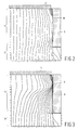
- Figure 2 illustrates a computer simulation of the current distribution in this mode for a device of the type described with reference to Figure I and having an off-state voltage rating of 600V where the second voltage across the anode and cathode electrodes A and K is 0.9V.
- the very low conductivity of the second subsidiary region 4b causes the difference between the hole quasi Fermi potential in the second subsidiary region 4b and the electron quasi Fermi potential in the inversion channel in the second subsidiary channel area 40b to become greater than the voltage barrier 0.7V between the inversion channel (in area 40b) and the second subsidiary region 4b causing the associated pn junction 40b' to become forward-biassed resulting in electrons being injected into the second subsidiary region 4b and so turning on the distributed NPN bipolar transistor defined by the inversion channel in area 40b acting as the emitter, the second subsidiary region 4b acting as the base and the drift region 3 acting as the collector, and leading with the injection from the anode region 8 to thyristor action.
- both the emitter/base and base/collector pn junctions of this distributed NPN transistor are connected by the subsidiary inversion channel formed in the area (40c) of the third subsidiary region 4c, the fraction of the electron current flowing through the subsidiary inversion channel in area 40c is negligible because of the relatively high resistance provided by the path through the subsidiary inversion channel in area 40c. Consequently, both the second subsidiary region 4b and the drift region 3 are highly modulated by mobile carriers, and at this stage the device la functions in a combined IGBT-thyristor mode as illustrated by the computer simulation derived for the device of Figure 1 with an anode voltage of 1.6 volts.
- the main fraction of the hole current flows through the second region 4 to the cathode electrode K while, as in a thyristor structure, the pn junction 40b' formed between the inversion channel in 40b and the second subsidiary region 4b and the pn junction 5 between the third subsidiary region 4c and the drift region 3 are both forward-biassed (because under high injection the npn (regions 40b, 4b, 3) transistor is saturated) allowing the thyristor current to flow through the entire thyristor structure bypassing the inversion channels in areas 40b and 40c. The effective length of the inversion channel is thus reduced to that of the subsidiary inversion channel in area 40a.
- the relatively highly doped third subsidiary region 4c serves to prevent punch-through between the third and first regions 6 and 3 when the device is in a reverse voltage blocking condition (that is when no gate voltage is applied so enabling the doping concentration within the second subsidiary region 4b and the channel length to be as low as desired without having to worry unduly about punch-through problems.
- This enables, on the assumption that first subsidiary region 4a is highly conductive to inhibit injection at the pn junction 7, the length and the impurity concentration level of the first and second subsidiary channel areas 40a and 40b to be substantially reduced provided that the second subsidiary region 40b can still provide sufficient electron injection for thyristor action.
- the current density tends to saturate because of, for example, the decrease in carrier mobility in the inversion channel, pinch-off effects due to the saturation of the MOS transistor (whose channel region is provided by the inversion channel in area 40a and some of 40b) as the effective MOS drain voltage increases with the anode voltage.
- the device remains in the on-state for as long as an appropriate first voltage is applied to the gate electrode G.
- Turn-off of the device la is achieved by interrupting or removing the positive first voltage from the gate electrode G. This causes the collapse of the inversion channel and thus the removal of the thyristor emitter. During turn-off, the holes are extracted through the second region 4 to the cathode electrode K and any remaining excess injected carrier charge decreases with time by recombination.
- Figure 4 illustrates computer simulations of the anode current (IA) versus anode voltage (VA) characteristics for two devices la having the structure described above with reference to Figure 1 but with different effective channel lengths (where the effective channel length is the difference in depth below the surface 2a of the regions 6 and 4a) and a doping concentration in the second subsidiary region 4b of 10 14 ions cm -3 and two conventional trench gate IGBTs having a constant doping (10 17 ions cm -3 ) second region 4. In each case the gate or first voltage Vg is 15 volts.
- Line a illustrates the characteristic for a long channel trench IGBT which may have an off-state blocking voltage of 600 volts
- line b illustrates the characteristic for a short channel (0.5 ⁇ m) trench IGBT having a much lower off state blocking voltage than the trench IGBT illustrated by line a
- line c illustrates the characteristic for a short channel (0.5 ⁇ m) device la in accordance with Figure I and having an off-state blocking voltage of 600 volts
- line d illustrates the characteristic for a very short channel (0.2 ⁇ m) device la in accordance with Figure I and with an off-state blocking voltage equivalent to that of the device represented by line c.
- a very significant increase in current density compared to a IGBT and a characteristic very close to a thyristor characteristic can be achieved with a device in accordance with Figure 1.
- Figure I The device la shown in Figure I could be modified by being manufactured using planar technology by analogy with conventional IGBT structures as shown in, for example, US-A-4,364,073.
- Figure 5 illustrates a cross-sectional view through such a planar device Ib.
- the device Ib differs from the device la in that the third, second and first subsidiary regions 4a,4b and 4a of the second region 4 and the third region 6 are all formed as planar regions each meeting the major surface 2a and the insulated gate structure 9,10 is formed over the conduction channel area 40 on the major surface 2a.
- This structure may be formed by analogy with standard DMOSFET processing by introducing the impurities la form the third, second and first subsidiary regions 4c,4b and 4c of the second region 4 and the third regions 6 using the insulated gate structure as a mask.
- each cell may be masked from the introduction of the impurities to form the third regions as shown in Figure 5 or alternatively a moat may be etched in known fashion through the centre of each third region to expose an underlying area of the second region 4 before the metallisation to form the cathode electrode K is deposited.
- a relatively highly doped central fourth subsidiary region 4d (indicated by dashed lines) of the second region 4 may be formed, as is known to the person skilled in the art of power DMOSFET manufacture, prior to definition of the insulated gate structure 9,10 to enable ohmic contact to the second region 4 and to inhibit parasitic bipolar action.
- the doping, depths and widths of the various regions may be selected as desired bearing in mind that, as indicated above, the gains of the two parasitic bipolar transistors formed by the injector, first and second regions 8,3 and 4 and by the third, second and first regions 6,4 and 3 should add up to less than unity.
- the doping concentrations will be similar to those given above with reference to the device shown in Figure 1.
- the device Ib may consist of many hundreds or thousands of parallel-connected device cells each in this case consisting of a second region 4 and associated third region 6.
- Figure 6 illustrates a cross-sectional view through a third example of a device Ic in accordance with the invention.
- the device Ic shown in Figure 6 is a lateral device rather than a vertical device as shown in Figures 1 and 5.
- the main current path is between the major surfaces 2a and 2b (i.e. in a 'vertical' direction)
- the main current path is in a direction along or generally parallel to the major surfaces 2a and 2b (i.e. in a 'lateral' direction) because the anode and cathode electrodes A and K are both provided at the one major surface 2a.
- An insulating or passivating layer 15 may be provided on the other major surface 2b.
- the device Ic differs from that shown in Figure 5 mainly in the provision of the injector region at the major surface 2a rather than at the major surface 2b.
- this is a lateral device it is not necessary for relatively lowly doped second subsidiary region 4b to be formed within the relatively highly doped third subsidiary region 4c. Accordingly these various regions may be formed by use of appropriate masking and dopant introduction techniques without having to worry about forming a relatively lowly doped region (that is the second subsidiary region 4b) in a relatively highly doped region (for example the third subsidiary region).
- the relatively lowly doped second subsidiary region 4b may be implanted first and then the relatively highly doped subsidiary regions 4a and 4c (and 4d if present) formed by implantation through an appropriate mask.
- the device Ic shown in Figure 6 needs to be isolated from other similar parallel-connected structures which may be formed on the same substrate to form a power device.
- this is achieved by pn junction isolation, by providing the first or drift region 3 as an epitaxial layer on an opposite (in this case p) conductivity type substrate 20 and by using highly p conductivity doped regions 21 formed using conventional masking, implantation and diffusion techniques to extend through the semiconductor body 2 from the major surface 2a to the substrate 20 to define the drift region 3 as a discrete well.
- Alternative isolation techniques such as the use of insulating layers or silicon on insulator techniques could be considered.
- the various regions shown in Figure 6 may have similar doping profiles to the corresponding regions in Figure 1. They may have an extent along the major surface 2a similar to the thicknesses of the corresponding regions shown in Figure I except that in the case of the lateral device Ic shown in Figure 6 the 'length' 1 (equivalent to Ib thickness in Figure 1) of the drift region 3 may need to be reduced to achieve a reasonable packing density.
- the drift region 3 may in this example have a 'length' e.g. 40 ⁇ m with a buffer relatively highly doped region 3a (indicated by dashed lines in Figure 6) extending for a distance of 2 ⁇ m around the injection region 8a for a device Ic with a reverse voltage blocking capability of 500V.
- the relatively lowly doped third subsidiary region 4c may be extended (as shown in dashed lines in Figure 6) to meet the substrate 20.
- the electrical shorting by the second main electrode 12 of the third region 6 and the second region 4 may alternatively be accomplished by etching a moat through the third region to expose an underlying portion of the second region 4.
- Figure 7 illustrates a modification Id of the device Ic where the planar technology has been replaced by a trench type of technology to produce a device Id which is a lateral version of the device la.
- Figure 7 differs from Figure I in that the first, second and third subsidiary regions 4a,4b and 4a are formed as planar discrete regions (as in the example shown in Figure 5) through which the groove 14 extends. As in Figure 1, it is the thicknesses or depths of these regions rather than their lateral extents which define the conduction channel area.
- Such a trench lateral device id should allow for a greater packing density than the DMOS type lateral device Ic shown in Figure 6.
- the vertical trench device la has advantages over the vertical DMOS device Ib while the lateral DMOS device Ic has advantages over the lateral trench device Id.
- both the vertical trench structure device la and the lateral DMOS type structure device Ic provide for a conduction channel which is generally parallel to the thyristor conduction path so allowing for a greater proportion of the hole current to flow, through the second subsidiary region 4b generally parallel to the inversion channel in area 40b than in the different geometry structures shown in Figures 5 and 7.
- an increase the thickness second subsidiary region 4b may be desirable in the examples of Figures 5 and 7 to facilitate the rise of the hole quasi fermi potential in this region to 0.7V above the quasi Fermi electron potential in the inversion channel 40b to initiate bipolar action.
- the examples illustrated in Figures 1 and 6 are relatively simple technologically to manufacture.
- the examples illustrated in Figures 5 and 7 both require the formation of a relatively highly doped third subsidiary region 4c and a relatively lowly doped second subsidiary region 4b within that highly doped region. This may require the use of sophisticated implantation techniques to achieve a relatively high doping level at a desired depth below the semiconductor body surface 2a (for example as described in GB-A-1,587,773) or even the use of selective etching, implantation and selective epitaxial growth techniques.
- the present invention is applied to an enhancement mode device, that is a device in which the conduction channel is formed in the channel areas 40a, 40b, 40c as an inversion channel by the application of an appropriate polarity first voltage to the insulated gate 9,10
- an enhancement mode device that is a device in which the conduction channel is formed in the channel areas 40a, 40b, 40c as an inversion channel by the application of an appropriate polarity first voltage to the insulated gate 9,10
- a depletion mode device that is to a device in which the channel area 40a, 40b, 40c is of the one conductivity type (n conductivity type where the second region is of p conductivity type) to provide the conduction channel when the gate voltage is zero and in which the conduction channel is removed by the application of an appropriate polarity first voltage to the insulated gate 9,10.
- the conduction channel area of such a depletion mode device could be formed by ion implantation through the surface at which the insulated gate 9,10 is to be formed.
- the present invention has been described with reference to and is primarily intended for an IGBT-like structure, it may be possible to apply the present invention to a conventional MOS-like device, that is a device in which the third region 3 forms the source region, the first region 7 provides the drain drift regions and the at least one injector region 8 is omitted and replaced by a highly doped subsidiary region of the one conductivity type of the drain region.
- the device structure and doping concentrations should be such that the opposite conductivity type carrier (holes in the case of an n-channel MOS) leakage current across the pn junction 5 is sufficient to enable the pn junction 40b' to become forward-biassed as the drain voltage rises to turn on the bipolar transistor formed by the second subsidiary channel, the second subsidiary region 4b and the drain region.
- Such a device would initially act as a MOS transistor but with sufficiently high drain voltage would then function as a bipolar transistor which bipolar transistor could then be switched off easily by removal of the conduction channel.
- the present invention could be applied to semiconductor materials other than silicon, for example III-V materials or combinations of different semiconductor materials.
Landscapes
- Thyristors (AREA)
Claims (11)
- Halbleiteranordnung (1a ; 1b; 1c; 1d) mit einer Bipolarfeldeffektanordnung mit isoliertem Gate, welche einen Halbleiterkörper (2) vorsieht, der eine erste Zone (3) des einen Leitfähigkeitstyps, eine, einen ersten pn-Übergang (5) mit der ersten Zone (3) bildende, zweite Zone (4) des entgegengesetzten Leitfähigkeitstyps, eine dritte Zone (5) des einen Leitfähigkeitstyps, welche einen zweiten pn-Übergang (7) mit der zweiten Zone (4) bildet und durch die zweite Zone (4) von der ersten Zone (3) getrennt ist, ein isoliertes Gate (9,10), ein in der zweiten Zone (4) vorgesehenes und an das isolierte Gate (9,10) angrenzendes Kanalgebiet (40), welches durch das isolierte Gate (9,10) zwischen einem ersten Zustand, in welchem ein Leitungskanal des einen Leitfähigkeitstyps eine Leiterbahn für den Fluß von Ladungsträgern des einen Leitfähigkeitstyps zwischen der ersten und dritten Zone (3 und 6) vorsieht, und einem zweiten Zustand, in welchem der Leitungskanal aufgehoben wird, gatesteuerbar ist, aufweist, wobei die Anordnung so konzipiert ist, daß das Einsetzen der Bipolartransistorfunktion durch die erste, zweite und dritte Zone (3, 4 und 6) unterbunden wird, dadurch gekennzeichnet, daß das Kanalgebiet (40) ein erstes und zweites Zusatzkanalgebiet (40a und 40b) aufweist, um den jeweiligen ersten und zweiten Zusatzleitungskanal des einen Leitfähigkeitstyps in dem ersten Zustand des Kanalgebietes (40) vorzusehen, wobei das zweite Zusatzkanalgebiet (40b) durch das erste Zusatzkanalgebiet (40a) von der dritten Zone (6) beabstandet ist und schwächer als das erste Zusatzkanalgebiet (40a) dotiert ist, wobei der zweite Zusatzleitungskanal einen Bipolartransistor mit der zweiten und ersten Zone (4 und 3) bildet und wobei ein pn-Übergang (40b) zwischen dem zweiten Zusatzleitungskanal und der zweiten Zone (4) in Durchlaßrichtung vorgespannt ist, wenn ein Strom von Ladungsträgern des entgegengesetzten Leitfähigkeitstyps in der zweiten Zone (4) bei Betrieb der Anordnung einen vorgegebenen Wert erreicht, wodurch in dem durch den zweiten Zusatzleitungskanal, die zweite Zone und die erste Zone gebildeten Bipolartransistor die Bipolartransistorfunktion ausgelöst wird, welche bei Aufhebung des Leitungskanales endet.
- Halbleiteranordnung nach Anspruch 1, bei welcher die zweite Zone (4) eine, an das isolierte Gate (9,10) angrenzende, erste und zweite Zusatzzone (4a und 4b) aufweist, wobei das erste und zweite Kanalgebiet (40a und 40b) jeweils in der ersten und zweiten Zusatzzone (4a und 4b) angeordnet sind.
- Halbleiteranordnung nach Anspruch 2, bei welcher die zweite Zusatzzone (4b) von der ersten Zone (3) durch eine, in der zweiten Zone (4) enthaltene, dritte Zusatzzone (4c), welche stärker als die zweite Zusatzzone (4b) dotiert ist, getrennt ist.
- Halbleiteranordnung nach einem der Ansprüche 1, 2 oder 3, bei welcher die dritte Zone (6) gegen die zweite Zone (4) elektrisch kurzgeschlossen ist.
- Halbleiteranordnung nach einem der vorangegangenen Ansprüche, bei welcher der Halbleiterkörper (2) eine erste und zweite, sich gegenüberliegende Hauptoberfläche (2a und 2b) aufweist und der erste und zweite pn-Übergang (5 und 7) auf die erste Hauptoberfläche (2a) auftreffen, so daß das Kanalgebiet (40) an die erste Hauptoberfläche (2a) angrenzt und sich die isolierte Gatestruktur (9,10) auf der ersten Hauptoberfläche (2a) über dem Kanalgebiet (40) erstreckt.
- Halbleiteranordnung nach einem der Ansprüche 1 bis 4, bei welcher der Halbleiterkörper (2) eine erste und zweite, sich gegenüberliegende Hauptoberfläche (2a und 2b) aufweist, die dritte Zone (6) auf die erste Hauptoberfläche (2a) auftrifft und die isolierte Gatestruktur (9,10) in einer Vertiefung, welche sich von der ersten Hauptoberfläche (2a) durch die dritte und zweite Zone (4 und 6) in die erste Zone (3) erstreckt, ausgebildet ist.
- Halbleiteranordnung nach einem der vorangegangenen Ansprüche, bei welcher der Halbleiterkörper (2) eine erste und zweite, sich gegenüberliegende Hauptoberfläche (2a und 2b) aufweist und die dritte und erste Zone (6 und 3) auf die erste Hauptoberfläche (2a) des Halbleiterkörpers (2) auftreffen.
- Halbleiteranordnung nach einem der vorangegangenen Ansprüche, bei welcher der Halbleiterkörper (2) eine erste und zweite, sich gegenüberliegende Hauptoberfläche (2a und 2b) aufweist und die dritte und erste Zone (6 und 3) jeweils auf die erste und zweite Hauptoberfläche (2a und 2b) des Halbleiterkörpers (2) auftreffen.
- Halbleiteranordnung nach einem der Ansprüche 1 bis 6, bei welcher der Strom von Ladungsträgern des entgegengesetzten Leitfähigkeitstyps durch zumindest eine Injektorzone (8) des entgegengesetzten Leitfähigkeitstyps vorgesehen ist, welche in dem Halbleiterkörper (2) angeordnet ist und einen dritten pn-Übergang mit der ersten Zone (3) bildet, um Ladungsträger des entgegengesetzten Leitfähigkeitstyps in die erste Zone (3) zu injizieren, wobei die Anordnung so konzipiert ist, daß eine Auslösung der Thyristorfunktion durch die erste, zweite, dritte und Injektorzone (3, 4, 6 und 8) verhindert wird, und wobei der Stom von Ladungsträgern des entgegengesetzten Leitfähigkeitstyps in der zweiten Zone (4) aus der Injektion von Ladungsträgern des entgegengesetzten Leitfähigkeitstyps durch die mindestens eine Injektorzone resultiert und die Thyristorfunktion, welche bei Aufhebung des Leitungskanales endet, mit der mindestens einen Injektorzone (8) durch den, durch den zweiten Zusatzleitungskanal, die zweite Zone und die erste Zone bei Einsetzen der Bipolartransistorfunktion gebildeten Bipolartransistor ausgelöst wird.
- Halbleiteranordnung nach Anspruch 9, bei welcher der Halbleiterkörper (2) eine erste und zweite, sich gegenüberliegende Hauptoberfläche (2a und 2b) aufweist und die dritte und die Injektorzone (6 und 8) auf die erste Hauptoberfläche (2a) des Halbleiterkörpers (2) auftreffen.
- Halbleiteranordnung nach Anspruch 9, bei welcher der Halbleiterkörper (2) eine erste und zweite, sich gegenüberliegende Hauptoberfläche (2a und 2b) aufweist und die dritte und die Injektorzone (6 und 8) jeweils auf die erste und zweite Hauptoberfläche (2a und 2b) des Halbleiterkörpers (2) auftreffen.
Applications Claiming Priority (2)
| Application Number | Priority Date | Filing Date | Title |
|---|---|---|---|
| GB9313843 | 1993-07-05 | ||
| GB939313843A GB9313843D0 (en) | 1993-07-05 | 1993-07-05 | A semiconductor device comprising an insulated gate field effect transistor |
Publications (2)
| Publication Number | Publication Date |
|---|---|
| EP0633611A1 EP0633611A1 (de) | 1995-01-11 |
| EP0633611B1 true EP0633611B1 (de) | 1998-11-04 |
Family
ID=10738303
Family Applications (1)
| Application Number | Title | Priority Date | Filing Date |
|---|---|---|---|
| EP94201890A Expired - Lifetime EP0633611B1 (de) | 1993-07-05 | 1994-06-30 | Halbleiteranordnung mit einer Bipolarfeldeffektanordnung mit isoliertem Gate |
Country Status (5)
| Country | Link |
|---|---|
| US (1) | US5489787A (de) |
| EP (1) | EP0633611B1 (de) |
| JP (1) | JPH0758332A (de) |
| DE (1) | DE69414311T2 (de) |
| GB (1) | GB9313843D0 (de) |
Families Citing this family (65)
| Publication number | Priority date | Publication date | Assignee | Title |
|---|---|---|---|---|
| US6001678A (en) * | 1995-03-14 | 1999-12-14 | Mitsubishi Denki Kabushiki Kaisha | Insulated gate semiconductor device |
| DE69631995T2 (de) * | 1995-06-02 | 2005-02-10 | Siliconix Inc., Santa Clara | Bidirektional sperrender Graben-Leistungs-MOSFET |
| JP3384198B2 (ja) * | 1995-07-21 | 2003-03-10 | 三菱電機株式会社 | 絶縁ゲート型半導体装置およびその製造方法 |
| SE9601179D0 (sv) * | 1996-03-27 | 1996-03-27 | Abb Research Ltd | A field controlled semiconductor device of SiC and a method for production thereof |
| JPH09331062A (ja) * | 1996-06-11 | 1997-12-22 | Mitsubishi Electric Corp | 半導体装置およびその製造方法 |
| GB2321337B (en) * | 1997-01-21 | 2001-11-07 | Plessey Semiconductors Ltd | Improvements in or relating to semiconductor devices |
| US6060746A (en) * | 1997-02-11 | 2000-05-09 | International Business Machines Corporation | Power transistor having vertical FETs and method for making same |
| US6011279A (en) * | 1997-04-30 | 2000-01-04 | Cree Research, Inc. | Silicon carbide field controlled bipolar switch |
| JPH10335649A (ja) * | 1997-05-27 | 1998-12-18 | Mitsubishi Electric Corp | 半導体装置およびその製造方法 |
| US6121633A (en) * | 1997-06-12 | 2000-09-19 | Cree Research, Inc. | Latch-up free power MOS-bipolar transistor |
| US5969378A (en) * | 1997-06-12 | 1999-10-19 | Cree Research, Inc. | Latch-up free power UMOS-bipolar transistor |
| US5940689A (en) * | 1997-06-30 | 1999-08-17 | Harris Corporation | Method of fabricating UMOS semiconductor devices using a self-aligned, reduced mask process |
| US6096608A (en) * | 1997-06-30 | 2000-08-01 | Siliconix Incorporated | Bidirectional trench gated power mosfet with submerged body bus extending underneath gate trench |
| GB2327295A (en) * | 1997-07-11 | 1999-01-20 | Plessey Semiconductors Ltd | MOS controllable power semiconductor device |
| DE19804192A1 (de) * | 1998-02-03 | 1999-08-12 | Siemens Ag | Verfahren zur Herstellung eines Leistungshalbleiterbauelementes |
| GB9808234D0 (en) * | 1998-04-17 | 1998-06-17 | Koninkl Philips Electronics Nv | Mnufacture of trench-gate semiconductor devices |
| GB9808237D0 (en) * | 1998-04-17 | 1998-06-17 | Koninkl Philips Electronics Nv | Mnufacture of field-effect semiconductor devices |
| JP2000049338A (ja) * | 1998-07-28 | 2000-02-18 | Mitsubishi Electric Corp | 絶縁ゲート型トランジスタの特性評価方法、絶縁ゲート型トランジスタの製造方法、絶縁ゲート型トランジスタの特性評価装置、および特性評価プログラムを記録してあるコンピュータ読み取り可能な記録媒体 |
| KR100451450B1 (ko) * | 1998-12-18 | 2004-10-06 | 인피니언 테크놀로지스 아게 | 바디 영역내에 트렌치 형상의 게이트-전극 및 추가 고도핑 층을 갖는 전계 효과 트랜지스터 |
| US6373098B1 (en) * | 1999-05-25 | 2002-04-16 | Fairchild Semiconductor Corporation | Trench-gated device having trench walls formed by selective epitaxial growth and process for forming device |
| DE19945639A1 (de) * | 1999-09-23 | 2001-04-05 | Abb Semiconductors Ag | Bipolartransistor mit isolierter Gateelektrode (IGBT) |
| DE10009345C1 (de) * | 2000-02-28 | 2001-07-19 | Infineon Technologies Ag | Feldeffekt-Transistoranordnung mit hoher Latch-up-Festigkeit und Verfahren zu deren Herstellung |
| JP4371521B2 (ja) * | 2000-03-06 | 2009-11-25 | 株式会社東芝 | 電力用半導体素子およびその製造方法 |
| US6445037B1 (en) * | 2000-09-28 | 2002-09-03 | General Semiconductor, Inc. | Trench DMOS transistor having lightly doped source structure |
| DE10205323B4 (de) * | 2001-02-09 | 2011-03-24 | Fuji Electric Systems Co., Ltd. | Verfahren zur Herstellung eines Halbleiterbauelements |
| DE10205324B4 (de) * | 2001-02-09 | 2012-04-19 | Fuji Electric Co., Ltd. | Halbleiterbauelement |
| US20020179968A1 (en) * | 2001-05-30 | 2002-12-05 | Frank Pfirsch | Power semiconductor component, compensation component, power transistor, and method for producing power semiconductor components |
| DE10126308B4 (de) * | 2001-05-30 | 2008-02-21 | Infineon Technologies Ag | Rückwärtssperrender Leistungstransistor |
| JP4945055B2 (ja) * | 2003-08-04 | 2012-06-06 | ルネサスエレクトロニクス株式会社 | 半導体装置およびその製造方法 |
| EP1531497A1 (de) | 2003-11-17 | 2005-05-18 | ABB Technology AG | IGBT Kathodendesign mit verbessertem Sicherheitsbetriebsbereich |
| DE10361135B4 (de) * | 2003-12-23 | 2006-07-27 | Infineon Technologies Ag | Trenchtransistor und Verfahren zur Herstellung eines Trenchtransistors mit hochenergieimplantiertem Drain |
| JP2005340626A (ja) * | 2004-05-28 | 2005-12-08 | Toshiba Corp | 半導体装置 |
| US8362547B2 (en) | 2005-02-11 | 2013-01-29 | Alpha & Omega Semiconductor Limited | MOS device with Schottky barrier controlling layer |
| US8093651B2 (en) * | 2005-02-11 | 2012-01-10 | Alpha & Omega Semiconductor Limited | MOS device with integrated schottky diode in active region contact trench |
| US7948029B2 (en) * | 2005-02-11 | 2011-05-24 | Alpha And Omega Semiconductor Incorporated | MOS device with varying trench depth |
| US7285822B2 (en) * | 2005-02-11 | 2007-10-23 | Alpha & Omega Semiconductor, Inc. | Power MOS device |
| US8283723B2 (en) * | 2005-02-11 | 2012-10-09 | Alpha & Omega Semiconductor Limited | MOS device with low injection diode |
| US8779465B2 (en) * | 2006-09-22 | 2014-07-15 | Freescale Semiconductor, Inc. | Semiconductor device and method of forming a semiconductor device |
| JP2007173878A (ja) * | 2007-03-28 | 2007-07-05 | Toshiba Corp | 半導体装置 |
| CN100580905C (zh) * | 2007-04-20 | 2010-01-13 | 晶能光电(江西)有限公司 | 获得在分割衬底上制造的半导体器件的高质量边界的方法 |
| CN101868856B (zh) * | 2007-09-21 | 2014-03-12 | 飞兆半导体公司 | 用于功率器件的超结结构及制造方法 |
| US20120273916A1 (en) | 2011-04-27 | 2012-11-01 | Yedinak Joseph A | Superjunction Structures for Power Devices and Methods of Manufacture |
| JP4957840B2 (ja) | 2010-02-05 | 2012-06-20 | 株式会社デンソー | 絶縁ゲート型半導体装置 |
| JP2012099601A (ja) | 2010-11-01 | 2012-05-24 | Sumitomo Electric Ind Ltd | 半導体装置およびその製造方法 |
| US9105495B2 (en) | 2011-02-12 | 2015-08-11 | Freescale Semiconductor, Inc. | Semiconductor device and related fabrication methods |
| US8673700B2 (en) | 2011-04-27 | 2014-03-18 | Fairchild Semiconductor Corporation | Superjunction structures for power devices and methods of manufacture |
| US8772868B2 (en) | 2011-04-27 | 2014-07-08 | Fairchild Semiconductor Corporation | Superjunction structures for power devices and methods of manufacture |
| US8786010B2 (en) | 2011-04-27 | 2014-07-22 | Fairchild Semiconductor Corporation | Superjunction structures for power devices and methods of manufacture |
| US8836028B2 (en) | 2011-04-27 | 2014-09-16 | Fairchild Semiconductor Corporation | Superjunction structures for power devices and methods of manufacture |
| CN103021856A (zh) * | 2011-09-28 | 2013-04-03 | 比亚迪股份有限公司 | 具有超级结的半导体结构的形成方法及半导体结构 |
| US8872278B2 (en) | 2011-10-25 | 2014-10-28 | Fairchild Semiconductor Corporation | Integrated gate runner and field implant termination for trench devices |
| DE112012005981B4 (de) * | 2012-03-05 | 2025-04-30 | Mitsubishi Electric Corporation | Halbleitervorrichtungen |
| CN103578983A (zh) * | 2012-08-01 | 2014-02-12 | 无锡华润上华半导体有限公司 | 场中止型绝缘栅型双极晶体管及其制造方法 |
| JP6048317B2 (ja) * | 2013-06-05 | 2016-12-21 | 株式会社デンソー | 炭化珪素半導体装置 |
| CN104299907A (zh) * | 2013-07-19 | 2015-01-21 | 北大方正集团有限公司 | Vdmos器件的制作方法 |
| CN104795327B (zh) * | 2014-01-16 | 2017-12-15 | 北大方正集团有限公司 | 一种制作平面型vdmos的方法及平面型vdmos |
| JP6237408B2 (ja) * | 2014-03-28 | 2017-11-29 | 住友電気工業株式会社 | 炭化珪素半導体装置およびその製造方法 |
| CN104409485B (zh) * | 2014-12-05 | 2018-10-23 | 国家电网公司 | 具有低反向传输电容抗闩锁结构的平面栅igbt及其制造方法 |
| CN107546257A (zh) * | 2017-08-23 | 2018-01-05 | 恒泰柯半导体(上海)有限公司 | 金属‑氧化物沟道半导体场效应晶体管的外延层结构 |
| DE102018123210B3 (de) * | 2018-09-20 | 2020-02-27 | Infineon Technologies Ag | Siliziumkarbid-Bauelemente und Verfahren zum Bilden von Siliziumkarbid-Bauelementen |
| CN109599433A (zh) * | 2018-12-10 | 2019-04-09 | 泉州臻美智能科技有限公司 | 一种金属氧化物半导体关断晶闸管及其制作方法 |
| JP7396000B2 (ja) * | 2019-12-02 | 2023-12-12 | 富士電機株式会社 | 炭化珪素半導体装置 |
| GB2592928B (en) * | 2020-03-10 | 2025-01-29 | Mqsemi Ag | Insulated gate switched transistor |
| CN114927561B (zh) * | 2022-06-30 | 2023-05-02 | 电子科技大学 | 一种碳化硅mosfet器件 |
| CN115632060A (zh) * | 2022-10-28 | 2023-01-20 | 华虹半导体(无锡)有限公司 | 半导体结构及其形成方法 |
Family Cites Families (12)
| Publication number | Priority date | Publication date | Assignee | Title |
|---|---|---|---|---|
| DE2703877C2 (de) * | 1977-01-31 | 1982-06-03 | Siemens Ag, 1000 Berlin Und 8000 Muenchen | MIS-Transistor von kurzer Kanallänge und Verfahren zu seiner Herstellung |
| FR2422258A1 (fr) * | 1978-01-19 | 1979-11-02 | Radiotechnique Compelec | Dispositif semiconducteur monolithique a transistors de types mos et bipolaire |
| US4282478A (en) * | 1978-10-03 | 1981-08-04 | Rca Corporation | Reference current supply circuits |
| DE3024015A1 (de) * | 1980-06-26 | 1982-01-07 | Siemens AG, 1000 Berlin und 8000 München | Steuerbarer halbleiterschalter |
| US4969028A (en) * | 1980-12-02 | 1990-11-06 | General Electric Company | Gate enhanced rectifier |
| DE3224618A1 (de) * | 1982-07-01 | 1984-01-05 | Siemens AG, 1000 Berlin und 8000 München | Igfet mit ladungstraegerinjektion |
| US5016076A (en) * | 1990-02-28 | 1991-05-14 | At&T Bell Laboratories | Lateral MOS controlled thyristor |
| US5202750A (en) * | 1990-04-09 | 1993-04-13 | U.S. Philips Corp. | MOS-gated thyristor |
| US5151762A (en) * | 1990-04-12 | 1992-09-29 | Mitsubishi Denki Kabushiki Kaisha | Semiconductor device, fabricating method thereof and flash control device using the semiconductor device |
| JP2504862B2 (ja) * | 1990-10-08 | 1996-06-05 | 三菱電機株式会社 | 半導体装置及びその製造方法 |
| JP3163677B2 (ja) * | 1991-09-24 | 2001-05-08 | 富士電機株式会社 | Misfet制御型サイリスタを有する半導体装置 |
| US5321281A (en) * | 1992-03-18 | 1994-06-14 | Mitsubishi Denki Kabushiki Kaisha | Insulated gate semiconductor device and method of fabricating same |
-
1993
- 1993-07-05 GB GB939313843A patent/GB9313843D0/en active Pending
-
1994
- 1994-06-30 DE DE69414311T patent/DE69414311T2/de not_active Expired - Fee Related
- 1994-06-30 EP EP94201890A patent/EP0633611B1/de not_active Expired - Lifetime
- 1994-07-05 JP JP6153628A patent/JPH0758332A/ja active Pending
- 1994-07-06 US US08/271,407 patent/US5489787A/en not_active Expired - Fee Related
Also Published As
| Publication number | Publication date |
|---|---|
| DE69414311T2 (de) | 1999-06-02 |
| GB9313843D0 (en) | 1993-08-18 |
| DE69414311D1 (de) | 1998-12-10 |
| EP0633611A1 (de) | 1995-01-11 |
| US5489787A (en) | 1996-02-06 |
| JPH0758332A (ja) | 1995-03-03 |
Similar Documents
| Publication | Publication Date | Title |
|---|---|---|
| EP0633611B1 (de) | Halbleiteranordnung mit einer Bipolarfeldeffektanordnung mit isoliertem Gate | |
| KR100869324B1 (ko) | 베이스 리치-쓰루를 방지하는 측면 확장 베이스 차폐영역을 구비한 전력 반도체 소자 및 그 제조방법 | |
| US5637898A (en) | Vertical field effect transistors having improved breakdown voltage capability and low on-state resistance | |
| EP1396030B1 (de) | Vertikale Leistungshalbleiteranordnung und Verfahren zu deren Herstellung | |
| EP0737365B1 (de) | Drei-anschlussklemmen-gategesteuerte halbleiterschalteranordnung mit gleichrichtergate | |
| JP2005510059A (ja) | 電界効果トランジスタ半導体デバイス | |
| KR20010080325A (ko) | 개선된 고주파 스위칭 특성 및 항복 특성을 갖는 전력용반도체 장치들 | |
| WO2008156674A1 (en) | Improved power switching transistors | |
| US5879967A (en) | Methods forming power semiconductor devices having latch-up inhibiting regions | |
| JPH10209432A (ja) | 半導体デバイスの改良 | |
| KR100317458B1 (ko) | 선형 전류-전압특성을 가진 반도체 소자 | |
| US20220173227A1 (en) | Finfet power semiconductor devices | |
| GB2305777A (en) | Base resistance controlled thyristor structure with high density layout for increased current capacity | |
| US5912497A (en) | Semiconductor switching devices having buried gate electrodes and methods of forming same | |
| EP0454201B1 (de) | Halbleiteranordnung mit einem Thyristor | |
| US6084254A (en) | Lateral bipolar mode field effect transistor | |
| US11610987B2 (en) | NPNP layered MOS-gated trench device having lowered operating voltage | |
| US20250081491A1 (en) | Trench-gated switch with epitaxial p-body layer having higher doped top portion | |
| EP4187615A1 (de) | Pnp-schicht-mos-gate-grabenanordnung mit verringerter betriebsspannung | |
| EP4394881B1 (de) | Halbleiterbauelement und verfahren zur herstellung eines halbleiterbauelements | |
| CN120614847B (zh) | 一种集成低势垒二极管的鳍式场效应晶体管及其制造方法 | |
| US12568666B2 (en) | Insulated gate turn-off device with short channel PMOS transistor | |
| JPH10229192A (ja) | 半導体スイッチ素子 | |
| WO2006025034A2 (en) | Semiconductor device |
Legal Events
| Date | Code | Title | Description |
|---|---|---|---|
| PUAI | Public reference made under article 153(3) epc to a published international application that has entered the european phase |
Free format text: ORIGINAL CODE: 0009012 |
|
| AK | Designated contracting states |
Kind code of ref document: A1 Designated state(s): DE FR GB IT NL |
|
| 17P | Request for examination filed |
Effective date: 19950711 |
|
| 17Q | First examination report despatched |
Effective date: 19961023 |
|
| GRAG | Despatch of communication of intention to grant |
Free format text: ORIGINAL CODE: EPIDOS AGRA |
|
| GRAG | Despatch of communication of intention to grant |
Free format text: ORIGINAL CODE: EPIDOS AGRA |
|
| GRAH | Despatch of communication of intention to grant a patent |
Free format text: ORIGINAL CODE: EPIDOS IGRA |
|
| GRAH | Despatch of communication of intention to grant a patent |
Free format text: ORIGINAL CODE: EPIDOS IGRA |
|
| GRAA | (expected) grant |
Free format text: ORIGINAL CODE: 0009210 |
|
| AK | Designated contracting states |
Kind code of ref document: B1 Designated state(s): DE FR GB IT NL |
|
| PG25 | Lapsed in a contracting state [announced via postgrant information from national office to epo] |
Ref country code: NL Free format text: LAPSE BECAUSE OF FAILURE TO SUBMIT A TRANSLATION OF THE DESCRIPTION OR TO PAY THE FEE WITHIN THE PRESCRIBED TIME-LIMIT Effective date: 19981104 |
|
| REF | Corresponds to: |
Ref document number: 69414311 Country of ref document: DE Date of ref document: 19981210 |
|
| ET | Fr: translation filed | ||
| ITF | It: translation for a ep patent filed | ||
| NLV1 | Nl: lapsed or annulled due to failure to fulfill the requirements of art. 29p and 29m of the patents act | ||
| PLBE | No opposition filed within time limit |
Free format text: ORIGINAL CODE: 0009261 |
|
| STAA | Information on the status of an ep patent application or granted ep patent |
Free format text: STATUS: NO OPPOSITION FILED WITHIN TIME LIMIT |
|
| 26N | No opposition filed | ||
| REG | Reference to a national code |
Ref country code: GB Ref legal event code: IF02 |
|
| PGFP | Annual fee paid to national office [announced via postgrant information from national office to epo] |
Ref country code: FR Payment date: 20020625 Year of fee payment: 9 |
|
| PGFP | Annual fee paid to national office [announced via postgrant information from national office to epo] |
Ref country code: GB Payment date: 20020628 Year of fee payment: 9 |
|
| PGFP | Annual fee paid to national office [announced via postgrant information from national office to epo] |
Ref country code: DE Payment date: 20020821 Year of fee payment: 9 |
|
| PG25 | Lapsed in a contracting state [announced via postgrant information from national office to epo] |
Ref country code: GB Free format text: LAPSE BECAUSE OF NON-PAYMENT OF DUE FEES Effective date: 20030630 |
|
| PG25 | Lapsed in a contracting state [announced via postgrant information from national office to epo] |
Ref country code: DE Free format text: LAPSE BECAUSE OF NON-PAYMENT OF DUE FEES Effective date: 20040101 |
|
| GBPC | Gb: european patent ceased through non-payment of renewal fee |
Effective date: 20030630 |
|
| PG25 | Lapsed in a contracting state [announced via postgrant information from national office to epo] |
Ref country code: FR Free format text: LAPSE BECAUSE OF NON-PAYMENT OF DUE FEES Effective date: 20040227 |
|
| REG | Reference to a national code |
Ref country code: FR Ref legal event code: ST |
|
| PG25 | Lapsed in a contracting state [announced via postgrant information from national office to epo] |
Ref country code: IT Free format text: LAPSE BECAUSE OF NON-PAYMENT OF DUE FEES;WARNING: LAPSES OF ITALIAN PATENTS WITH EFFECTIVE DATE BEFORE 2007 MAY HAVE OCCURRED AT ANY TIME BEFORE 2007. THE CORRECT EFFECTIVE DATE MAY BE DIFFERENT FROM THE ONE RECORDED. Effective date: 20050630 |