EP0634792A2 - In Harz versiegelte Halbleitervorrichtung bestehend aus porösem Fluorkohlenstoffharz - Google Patents
In Harz versiegelte Halbleitervorrichtung bestehend aus porösem Fluorkohlenstoffharz Download PDFInfo
- Publication number
- EP0634792A2 EP0634792A2 EP94115972A EP94115972A EP0634792A2 EP 0634792 A2 EP0634792 A2 EP 0634792A2 EP 94115972 A EP94115972 A EP 94115972A EP 94115972 A EP94115972 A EP 94115972A EP 0634792 A2 EP0634792 A2 EP 0634792A2
- Authority
- EP
- European Patent Office
- Prior art keywords
- resin
- chip
- porous fluororesin
- fluororesin
- semiconductor device
- Prior art date
- Legal status (The legal status is an assumption and is not a legal conclusion. Google has not performed a legal analysis and makes no representation as to the accuracy of the status listed.)
- Granted
Links
Images
Classifications
-
- H—ELECTRICITY
- H10—SEMICONDUCTOR DEVICES; ELECTRIC SOLID-STATE DEVICES NOT OTHERWISE PROVIDED FOR
- H10W—GENERIC PACKAGES, INTERCONNECTIONS, CONNECTORS OR OTHER CONSTRUCTIONAL DETAILS OF DEVICES COVERED BY CLASS H10
- H10W74/00—Encapsulations, e.g. protective coatings
- H10W74/40—Encapsulations, e.g. protective coatings characterised by their materials
- H10W74/47—Encapsulations, e.g. protective coatings characterised by their materials comprising organic materials, e.g. plastics or resins
-
- H—ELECTRICITY
- H10—SEMICONDUCTOR DEVICES; ELECTRIC SOLID-STATE DEVICES NOT OTHERWISE PROVIDED FOR
- H10W—GENERIC PACKAGES, INTERCONNECTIONS, CONNECTORS OR OTHER CONSTRUCTIONAL DETAILS OF DEVICES COVERED BY CLASS H10
- H10W70/00—Package substrates; Interposers; Redistribution layers [RDL]
- H10W70/40—Leadframes
- H10W70/456—Materials
- H10W70/458—Materials of insulating layers on leadframes
-
- H—ELECTRICITY
- H10—SEMICONDUCTOR DEVICES; ELECTRIC SOLID-STATE DEVICES NOT OTHERWISE PROVIDED FOR
- H10W—GENERIC PACKAGES, INTERCONNECTIONS, CONNECTORS OR OTHER CONSTRUCTIONAL DETAILS OF DEVICES COVERED BY CLASS H10
- H10W74/00—Encapsulations, e.g. protective coatings
- H10W74/40—Encapsulations, e.g. protective coatings characterised by their materials
- H10W74/47—Encapsulations, e.g. protective coatings characterised by their materials comprising organic materials, e.g. plastics or resins
- H10W74/473—Encapsulations, e.g. protective coatings characterised by their materials comprising organic materials, e.g. plastics or resins containing a filler
-
- H—ELECTRICITY
- H10—SEMICONDUCTOR DEVICES; ELECTRIC SOLID-STATE DEVICES NOT OTHERWISE PROVIDED FOR
- H10W—GENERIC PACKAGES, INTERCONNECTIONS, CONNECTORS OR OTHER CONSTRUCTIONAL DETAILS OF DEVICES COVERED BY CLASS H10
- H10W72/00—Interconnections or connectors in packages
- H10W72/50—Bond wires
- H10W72/551—Materials of bond wires
- H10W72/552—Materials of bond wires comprising metals or metalloids, e.g. silver
- H10W72/5522—Materials of bond wires comprising metals or metalloids, e.g. silver comprising gold [Au]
-
- H—ELECTRICITY
- H10—SEMICONDUCTOR DEVICES; ELECTRIC SOLID-STATE DEVICES NOT OTHERWISE PROVIDED FOR
- H10W—GENERIC PACKAGES, INTERCONNECTIONS, CONNECTORS OR OTHER CONSTRUCTIONAL DETAILS OF DEVICES COVERED BY CLASS H10
- H10W74/00—Encapsulations, e.g. protective coatings
-
- H—ELECTRICITY
- H10—SEMICONDUCTOR DEVICES; ELECTRIC SOLID-STATE DEVICES NOT OTHERWISE PROVIDED FOR
- H10W—GENERIC PACKAGES, INTERCONNECTIONS, CONNECTORS OR OTHER CONSTRUCTIONAL DETAILS OF DEVICES COVERED BY CLASS H10
- H10W90/00—Package configurations
- H10W90/701—Package configurations characterised by the relative positions of pads or connectors relative to package parts
- H10W90/751—Package configurations characterised by the relative positions of pads or connectors relative to package parts of bond wires
- H10W90/756—Package configurations characterised by the relative positions of pads or connectors relative to package parts of bond wires between a chip and a stacked lead frame, conducting package substrate or heat sink
Definitions
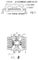
- a semiconductor element or chip 10 is mounted on a chip-mounting component 1 and the electrodes of the semiconductor chip connected to leads 2 by means of thin gold wires 4, which have excellent electrical characteristics.
- small pieces of porous fluororesin are incorporated into the molding resin surrounding the electional components.
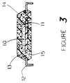
- a semiconductor chip 10 is mounted on a chip-mounting element 11 and the electrodes of chip 10 connected to leads 12 by means of thin gold wires 14 in the same manner as conventional devices.
- the circumference of the chip-mounting element 11 is enclosed and sealed by a molding resin 13 which contains small pieces 15 of a porous fluororesin.
- the size of the pieces are 1 to 500 microns (preferably 10 to 100 microns) of a porosity of 20 to 90 % (preferably 60 to 80 %) (calculated from the density of the resin). Even in cases when pieces 15 are incorporated into the molding resin 13 in an amount of 5 to 90 % by volume, the fine pores, although transmitting vapor and other gases, do not transmit liquids, thereby precluding the resin from penetrating inside the porous structure of the particles. The fine pores are retained unchanged. Therefore, the vapor that is generated by rapid heating during solder mounting is effectively absorbed in these fine pores.
- the present invention it is possible to securely prevent crack formation by alleviating and absorbing in small pieces of porous fluororesin the stress that is created in a resin layer when vapor is generated or the temperature is changed as a result of rapid heating during solder mounting of a resin-sealed semiconductor device. It is also possible to suppress to a minimum the formation of cracks and to lower the dielectric constant, thereby ensuring, among other effects, an increase in the speed with which signals are transmitted in semiconductor devices. Additionally, the devices have relatively thin-layer films and manufacture is not complex or expensive.
Landscapes
- Structures Or Materials For Encapsulating Or Coating Semiconductor Devices Or Solid State Devices (AREA)
Applications Claiming Priority (5)
| Application Number | Priority Date | Filing Date | Title |
|---|---|---|---|
| JP3067530A JPH04280660A (ja) | 1991-03-08 | 1991-03-08 | 樹脂封止型半導体装置 |
| JP67530/91 | 1991-03-08 | ||
| JP70378/91 | 1991-03-12 | ||
| JP3070378A JPH0722544A (ja) | 1991-03-12 | 1991-03-12 | 樹脂封止型半導体装置 |
| EP19920103297 EP0504634A3 (en) | 1991-03-08 | 1992-02-26 | Resin-sealed semiconductor device containing porous fluorocarbon resin |
Related Parent Applications (2)
| Application Number | Title | Priority Date | Filing Date |
|---|---|---|---|
| EP92103297.5 Division | 1992-02-26 | ||
| EP19920103297 Division EP0504634A3 (en) | 1991-03-08 | 1992-02-26 | Resin-sealed semiconductor device containing porous fluorocarbon resin |
Publications (3)
| Publication Number | Publication Date |
|---|---|
| EP0634792A2 true EP0634792A2 (de) | 1995-01-18 |
| EP0634792A3 EP0634792A3 (de) | 1995-07-12 |
| EP0634792B1 EP0634792B1 (de) | 1998-04-29 |
Family
ID=26408754
Family Applications (2)
| Application Number | Title | Priority Date | Filing Date |
|---|---|---|---|
| EP94115972A Expired - Lifetime EP0634792B1 (de) | 1991-03-08 | 1992-02-26 | In Harz versiegelte Halbleitervorrichtung bestehend aus porösem Fluorkohlenstoffharz |
| EP19920103297 Withdrawn EP0504634A3 (en) | 1991-03-08 | 1992-02-26 | Resin-sealed semiconductor device containing porous fluorocarbon resin |
Family Applications After (1)
| Application Number | Title | Priority Date | Filing Date |
|---|---|---|---|
| EP19920103297 Withdrawn EP0504634A3 (en) | 1991-03-08 | 1992-02-26 | Resin-sealed semiconductor device containing porous fluorocarbon resin |
Country Status (3)
| Country | Link |
|---|---|
| US (1) | US5446315A (de) |
| EP (2) | EP0634792B1 (de) |
| DE (1) | DE69225337T2 (de) |
Families Citing this family (12)
| Publication number | Priority date | Publication date | Assignee | Title |
|---|---|---|---|---|
| KR0148080B1 (ko) * | 1995-07-31 | 1998-08-01 | 김광호 | 반도체 리드프레임 제조방법 및 그를 이용한 반도체 칩 패키지 제조방법 |
| US6791194B1 (en) * | 1996-05-30 | 2004-09-14 | Hitachi, Ltd. | Circuit tape having adhesive film, semiconductor device, and a method for manufacturing the same |
| US5910341A (en) * | 1996-10-31 | 1999-06-08 | International Business Machines Corporation | Method of controlling the spread of an adhesive on a circuitized organic substrate |
| US5766979A (en) * | 1996-11-08 | 1998-06-16 | W. L. Gore & Associates, Inc. | Wafer level contact sheet and method of assembly |
| US5909123A (en) * | 1996-11-08 | 1999-06-01 | W. L. Gore & Associates, Inc. | Method for performing reliability screening and burn-in of semi-conductor wafers |
| JP3639088B2 (ja) * | 1997-06-06 | 2005-04-13 | 株式会社ルネサステクノロジ | 半導体装置及び配線テープ |
| US6080932A (en) * | 1998-04-14 | 2000-06-27 | Tessera, Inc. | Semiconductor package assemblies with moisture vents |
| US6414383B1 (en) * | 1999-07-16 | 2002-07-02 | Agere Systems Guardian Corp. | Very low magnetic field integrated circuit |
| JP4796235B2 (ja) * | 2001-03-27 | 2011-10-19 | 上野製薬株式会社 | ビナフトール誘導体金属塩およびその製法 |
| SE0101107D0 (sv) * | 2001-03-28 | 2001-03-28 | Ericsson Telefon Ab L M | Encapsulation arrangement |
| US7045885B1 (en) | 2004-12-09 | 2006-05-16 | Hewlett-Packard Development Company, L.P. | Placement of absorbing material in a semiconductor device |
| US7435625B2 (en) * | 2005-10-24 | 2008-10-14 | Freescale Semiconductor, Inc. | Semiconductor device with reduced package cross-talk and loss |
Family Cites Families (26)
| Publication number | Priority date | Publication date | Assignee | Title |
|---|---|---|---|---|
| NL268830A (de) * | 1960-12-01 | |||
| US3670091A (en) * | 1971-05-20 | 1972-06-13 | Sqrague Electric Co | Encapsulated electrical components with protective pre-coat containing collapsible microspheres |
| JPS5650545A (en) * | 1979-10-01 | 1981-05-07 | Hitachi Ltd | Resin molded type semiconductor device |
| JPS6018145B2 (ja) * | 1980-09-22 | 1985-05-09 | 株式会社日立製作所 | 樹脂封止型半導体装置 |
| JPS59186351A (ja) * | 1983-04-06 | 1984-10-23 | Mitsubishi Electric Corp | 半導体樹脂封止法 |
| JPS6123348A (ja) * | 1984-07-12 | 1986-01-31 | Nec Corp | 樹脂封止型半導体装置 |
| JPS61292943A (ja) * | 1985-06-21 | 1986-12-23 | Hitachi Ltd | 樹脂封止型半導体装置用充てん材 |
| JPS6315448A (ja) * | 1986-07-07 | 1988-01-22 | Nitto Electric Ind Co Ltd | 半導体装置 |
| JPS6347958A (ja) * | 1986-08-18 | 1988-02-29 | Toshiba Corp | 樹脂封止型半導体装置 |
| JPS63207811A (ja) * | 1987-02-25 | 1988-08-29 | Nippon Steel Chem Co Ltd | 半導体封止用樹脂組成物 |
| US4888634A (en) * | 1987-07-24 | 1989-12-19 | Linear Technology Corporation | High thermal resistance bonding material and semiconductor structures using same |
| JPS6436056A (en) * | 1987-07-31 | 1989-02-07 | Oki Electric Ind Co Ltd | Semiconductor device |
| JPH01208846A (ja) * | 1988-02-16 | 1989-08-22 | Hitachi Ltd | 半導体装置 |
| JPH01261451A (ja) * | 1988-04-12 | 1989-10-18 | Fujitsu Ltd | 半導体装置等用エポキシ樹脂封止組成物 |
| JPH0210858A (ja) * | 1988-06-29 | 1990-01-16 | Mitsubishi Electric Corp | 樹脂封止型半導体装置 |
| US4985751A (en) * | 1988-09-13 | 1991-01-15 | Shin-Etsu Chemical Co., Ltd. | Resin-encapsulated semiconductor devices |
| JPH02125644A (ja) * | 1988-11-05 | 1990-05-14 | Seiko Epson Corp | 樹脂封止半導体装置 |
| JPH02178953A (ja) * | 1988-12-29 | 1990-07-11 | Nec Corp | 樹脂封止型半導体装置 |
| JPH0821579B2 (ja) * | 1989-04-19 | 1996-03-04 | 旭硝子株式会社 | 半導体素子・集積回路装置 |
| JPH0324119A (ja) * | 1989-06-22 | 1991-02-01 | Toshiba Chem Corp | 封止用樹脂組成物及び半導体封止装置 |
| JPH0327557A (ja) * | 1989-06-23 | 1991-02-05 | Fujitsu Ltd | 半導体装置 |
| US5034801A (en) * | 1989-07-31 | 1991-07-23 | W. L. Gore & Associates, Inc. | Intergrated circuit element having a planar, solvent-free dielectric layer |
| US5015675A (en) * | 1989-07-31 | 1991-05-14 | General Electric Company | Encapsulation method, microelectronic devices made therefrom, and heat curable compositions based on epoxy resins, diaryliodonium hexafluroantimonate salts and free radical generators |
| JP2712618B2 (ja) * | 1989-09-08 | 1998-02-16 | 三菱電機株式会社 | 樹脂封止型半導体装置 |
| JPH03125644A (ja) * | 1989-10-09 | 1991-05-29 | Endo Takahisa | 改良型ドアミラー |
| US5122858A (en) * | 1990-09-10 | 1992-06-16 | Olin Corporation | Lead frame having polymer coated surface portions |
-
1992
- 1992-02-26 EP EP94115972A patent/EP0634792B1/de not_active Expired - Lifetime
- 1992-02-26 DE DE69225337T patent/DE69225337T2/de not_active Expired - Fee Related
- 1992-02-26 EP EP19920103297 patent/EP0504634A3/en not_active Withdrawn
-
1994
- 1994-01-11 US US08/182,520 patent/US5446315A/en not_active Expired - Lifetime
Also Published As
| Publication number | Publication date |
|---|---|
| EP0504634A2 (de) | 1992-09-23 |
| EP0504634A3 (en) | 1994-06-01 |
| DE69225337D1 (de) | 1998-06-04 |
| DE69225337T2 (de) | 1998-08-27 |
| US5446315A (en) | 1995-08-29 |
| EP0634792A3 (de) | 1995-07-12 |
| EP0634792B1 (de) | 1998-04-29 |
Similar Documents
| Publication | Publication Date | Title |
|---|---|---|
| EP0634792B1 (de) | In Harz versiegelte Halbleitervorrichtung bestehend aus porösem Fluorkohlenstoffharz | |
| US5956233A (en) | High density single inline memory module | |
| US5756380A (en) | Method for making a moisture resistant semiconductor device having an organic substrate | |
| KR0156065B1 (ko) | 플립 칩 캐리어 모듈의 표면 실장 공정 | |
| US6049129A (en) | Chip size integrated circuit package | |
| US6891259B2 (en) | Semiconductor package having dam and method for fabricating the same | |
| US6551862B2 (en) | Semiconductor device and method of manufacturing the same | |
| US5311060A (en) | Heat sink for semiconductor device assembly | |
| US4926238A (en) | Semiconductor device and method for producing the same | |
| US6365833B1 (en) | Integrated circuit package | |
| CA1167571A (en) | Integrated circuit package | |
| US6054755A (en) | Semiconductor package with improved moisture vapor relief function and method of fabricating the same | |
| KR100206894B1 (ko) | 바지에이 패키지 | |
| Suhl | Thermally induced IC package cracking | |
| EP0971009B1 (de) | Klebstoffzusammensetzung zur Verklebung von Halbleiterchips | |
| US6320126B1 (en) | Vertical ball grid array integrated circuit package | |
| Iko et al. | Encapsulating resins for semiconductors | |
| EP1111667A1 (de) | Halbleitervorrichtung und herstellungsverfahren | |
| US6165816A (en) | Fabrication of electronic components having a hollow package structure with a ceramic lid | |
| JPH0722544A (ja) | 樹脂封止型半導体装置 | |
| US20050287350A1 (en) | Encapsulating compound having reduced dielectric constant | |
| KR100400028B1 (ko) | 칩-온-칩 구조의 전력용 반도체소자 | |
| JPH04280660A (ja) | 樹脂封止型半導体装置 | |
| US7652383B2 (en) | Semiconductor package module without a solder ball and method of manufacturing the semiconductor package module | |
| KR100652064B1 (ko) | Bga 패키지 |
Legal Events
| Date | Code | Title | Description |
|---|---|---|---|
| PUAI | Public reference made under article 153(3) epc to a published international application that has entered the european phase |
Free format text: ORIGINAL CODE: 0009012 |
|
| 17P | Request for examination filed |
Effective date: 19941010 |
|
| AC | Divisional application: reference to earlier application |
Ref document number: 504634 Country of ref document: EP |
|
| AK | Designated contracting states |
Kind code of ref document: A2 Designated state(s): DE FR GB IT SE |
|
| PUAL | Search report despatched |
Free format text: ORIGINAL CODE: 0009013 |
|
| AK | Designated contracting states |
Kind code of ref document: A3 Designated state(s): DE FR GB IT SE |
|
| GRAG | Despatch of communication of intention to grant |
Free format text: ORIGINAL CODE: EPIDOS AGRA |
|
| 17Q | First examination report despatched |
Effective date: 19970714 |
|
| GRAG | Despatch of communication of intention to grant |
Free format text: ORIGINAL CODE: EPIDOS AGRA |
|
| GRAH | Despatch of communication of intention to grant a patent |
Free format text: ORIGINAL CODE: EPIDOS IGRA |
|
| GRAH | Despatch of communication of intention to grant a patent |
Free format text: ORIGINAL CODE: EPIDOS IGRA |
|
| GRAA | (expected) grant |
Free format text: ORIGINAL CODE: 0009210 |
|
| AC | Divisional application: reference to earlier application |
Ref document number: 504634 Country of ref document: EP |
|
| AK | Designated contracting states |
Kind code of ref document: B1 Designated state(s): DE FR GB IT SE |
|
| ITF | It: translation for a ep patent filed | ||
| REF | Corresponds to: |
Ref document number: 69225337 Country of ref document: DE Date of ref document: 19980604 |
|
| ET | Fr: translation filed | ||
| PG25 | Lapsed in a contracting state [announced via postgrant information from national office to epo] |
Ref country code: GB Free format text: LAPSE BECAUSE OF NON-PAYMENT OF DUE FEES Effective date: 19990226 |
|
| PG25 | Lapsed in a contracting state [announced via postgrant information from national office to epo] |
Ref country code: SE Free format text: LAPSE BECAUSE OF NON-PAYMENT OF DUE FEES Effective date: 19990227 |
|
| PLBE | No opposition filed within time limit |
Free format text: ORIGINAL CODE: 0009261 |
|
| STAA | Information on the status of an ep patent application or granted ep patent |
Free format text: STATUS: NO OPPOSITION FILED WITHIN TIME LIMIT |
|
| 26N | No opposition filed | ||
| GBPC | Gb: european patent ceased through non-payment of renewal fee |
Effective date: 19990226 |
|
| PG25 | Lapsed in a contracting state [announced via postgrant information from national office to epo] |
Ref country code: FR Free format text: LAPSE BECAUSE OF NON-PAYMENT OF DUE FEES Effective date: 19991029 |
|
| EUG | Se: european patent has lapsed |
Ref document number: 94115972.5 |
|
| PG25 | Lapsed in a contracting state [announced via postgrant information from national office to epo] |
Ref country code: DE Free format text: LAPSE BECAUSE OF NON-PAYMENT OF DUE FEES Effective date: 19991201 |
|
| REG | Reference to a national code |
Ref country code: FR Ref legal event code: ST |
|
| PG25 | Lapsed in a contracting state [announced via postgrant information from national office to epo] |
Ref country code: IT Free format text: LAPSE BECAUSE OF NON-PAYMENT OF DUE FEES;WARNING: LAPSES OF ITALIAN PATENTS WITH EFFECTIVE DATE BEFORE 2007 MAY HAVE OCCURRED AT ANY TIME BEFORE 2007. THE CORRECT EFFECTIVE DATE MAY BE DIFFERENT FROM THE ONE RECORDED. Effective date: 20050226 |