EP1111667A1 - Halbleitervorrichtung und herstellungsverfahren - Google Patents
Halbleitervorrichtung und herstellungsverfahren Download PDFInfo
- Publication number
- EP1111667A1 EP1111667A1 EP99931560A EP99931560A EP1111667A1 EP 1111667 A1 EP1111667 A1 EP 1111667A1 EP 99931560 A EP99931560 A EP 99931560A EP 99931560 A EP99931560 A EP 99931560A EP 1111667 A1 EP1111667 A1 EP 1111667A1
- Authority
- EP
- European Patent Office
- Prior art keywords
- semiconductor
- organic insulating
- adhesive
- semiconductor device
- insulating encapsulant
- Prior art date
- Legal status (The legal status is an assumption and is not a legal conclusion. Google has not performed a legal analysis and makes no representation as to the accuracy of the status listed.)
- Withdrawn
Links
Images


Classifications
-
- H—ELECTRICITY
- H10—SEMICONDUCTOR DEVICES; ELECTRIC SOLID-STATE DEVICES NOT OTHERWISE PROVIDED FOR
- H10W—GENERIC PACKAGES, INTERCONNECTIONS, CONNECTORS OR OTHER CONSTRUCTIONAL DETAILS OF DEVICES COVERED BY CLASS H10
- H10W72/00—Interconnections or connectors in packages
- H10W72/071—Connecting or disconnecting
-
- H—ELECTRICITY
- H10—SEMICONDUCTOR DEVICES; ELECTRIC SOLID-STATE DEVICES NOT OTHERWISE PROVIDED FOR
- H10W—GENERIC PACKAGES, INTERCONNECTIONS, CONNECTORS OR OTHER CONSTRUCTIONAL DETAILS OF DEVICES COVERED BY CLASS H10
- H10W74/00—Encapsulations, e.g. protective coatings
- H10W74/10—Encapsulations, e.g. protective coatings characterised by their shape or disposition
- H10W74/111—Encapsulations, e.g. protective coatings characterised by their shape or disposition the semiconductor body being completely enclosed
- H10W74/114—Encapsulations, e.g. protective coatings characterised by their shape or disposition the semiconductor body being completely enclosed by a substrate and the encapsulations
-
- H—ELECTRICITY
- H10—SEMICONDUCTOR DEVICES; ELECTRIC SOLID-STATE DEVICES NOT OTHERWISE PROVIDED FOR
- H10W—GENERIC PACKAGES, INTERCONNECTIONS, CONNECTORS OR OTHER CONSTRUCTIONAL DETAILS OF DEVICES COVERED BY CLASS H10
- H10W74/00—Encapsulations, e.g. protective coatings
- H10W74/10—Encapsulations, e.g. protective coatings characterised by their shape or disposition
- H10W74/111—Encapsulations, e.g. protective coatings characterised by their shape or disposition the semiconductor body being completely enclosed
- H10W74/114—Encapsulations, e.g. protective coatings characterised by their shape or disposition the semiconductor body being completely enclosed by a substrate and the encapsulations
- H10W74/117—Encapsulations, e.g. protective coatings characterised by their shape or disposition the semiconductor body being completely enclosed by a substrate and the encapsulations the substrate having spherical bumps for external connection
-
- H—ELECTRICITY
- H10—SEMICONDUCTOR DEVICES; ELECTRIC SOLID-STATE DEVICES NOT OTHERWISE PROVIDED FOR
- H10W—GENERIC PACKAGES, INTERCONNECTIONS, CONNECTORS OR OTHER CONSTRUCTIONAL DETAILS OF DEVICES COVERED BY CLASS H10
- H10W90/00—Package configurations
- H10W90/701—Package configurations characterised by the relative positions of pads or connectors relative to package parts
-
- H—ELECTRICITY
- H10—SEMICONDUCTOR DEVICES; ELECTRIC SOLID-STATE DEVICES NOT OTHERWISE PROVIDED FOR
- H10W—GENERIC PACKAGES, INTERCONNECTIONS, CONNECTORS OR OTHER CONSTRUCTIONAL DETAILS OF DEVICES COVERED BY CLASS H10
- H10W72/00—Interconnections or connectors in packages
- H10W72/071—Connecting or disconnecting
- H10W72/073—Connecting or disconnecting of die-attach connectors
-
- H—ELECTRICITY
- H10—SEMICONDUCTOR DEVICES; ELECTRIC SOLID-STATE DEVICES NOT OTHERWISE PROVIDED FOR
- H10W—GENERIC PACKAGES, INTERCONNECTIONS, CONNECTORS OR OTHER CONSTRUCTIONAL DETAILS OF DEVICES COVERED BY CLASS H10
- H10W72/00—Interconnections or connectors in packages
- H10W72/071—Connecting or disconnecting
- H10W72/073—Connecting or disconnecting of die-attach connectors
- H10W72/07321—Aligning
- H10W72/07327—Aligning involving guiding structures, e.g. spacers or supporting members
-
- H—ELECTRICITY
- H10—SEMICONDUCTOR DEVICES; ELECTRIC SOLID-STATE DEVICES NOT OTHERWISE PROVIDED FOR
- H10W—GENERIC PACKAGES, INTERCONNECTIONS, CONNECTORS OR OTHER CONSTRUCTIONAL DETAILS OF DEVICES COVERED BY CLASS H10
- H10W72/00—Interconnections or connectors in packages
- H10W72/071—Connecting or disconnecting
- H10W72/073—Connecting or disconnecting of die-attach connectors
- H10W72/07331—Connecting techniques
- H10W72/07337—Connecting techniques using a polymer adhesive, e.g. an adhesive based on silicone or epoxy
- H10W72/07338—Connecting techniques using a polymer adhesive, e.g. an adhesive based on silicone or epoxy hardening the adhesive by curing, e.g. thermosetting
-
- H—ELECTRICITY
- H10—SEMICONDUCTOR DEVICES; ELECTRIC SOLID-STATE DEVICES NOT OTHERWISE PROVIDED FOR
- H10W—GENERIC PACKAGES, INTERCONNECTIONS, CONNECTORS OR OTHER CONSTRUCTIONAL DETAILS OF DEVICES COVERED BY CLASS H10
- H10W72/00—Interconnections or connectors in packages
- H10W72/071—Connecting or disconnecting
- H10W72/075—Connecting or disconnecting of bond wires
-
- H—ELECTRICITY
- H10—SEMICONDUCTOR DEVICES; ELECTRIC SOLID-STATE DEVICES NOT OTHERWISE PROVIDED FOR
- H10W—GENERIC PACKAGES, INTERCONNECTIONS, CONNECTORS OR OTHER CONSTRUCTIONAL DETAILS OF DEVICES COVERED BY CLASS H10
- H10W72/00—Interconnections or connectors in packages
- H10W72/30—Die-attach connectors
-
- H—ELECTRICITY
- H10—SEMICONDUCTOR DEVICES; ELECTRIC SOLID-STATE DEVICES NOT OTHERWISE PROVIDED FOR
- H10W—GENERIC PACKAGES, INTERCONNECTIONS, CONNECTORS OR OTHER CONSTRUCTIONAL DETAILS OF DEVICES COVERED BY CLASS H10
- H10W72/00—Interconnections or connectors in packages
- H10W72/30—Die-attach connectors
- H10W72/321—Structures or relative sizes of die-attach connectors
- H10W72/325—Die-attach connectors having a filler embedded in a matrix
-
- H—ELECTRICITY
- H10—SEMICONDUCTOR DEVICES; ELECTRIC SOLID-STATE DEVICES NOT OTHERWISE PROVIDED FOR
- H10W—GENERIC PACKAGES, INTERCONNECTIONS, CONNECTORS OR OTHER CONSTRUCTIONAL DETAILS OF DEVICES COVERED BY CLASS H10
- H10W72/00—Interconnections or connectors in packages
- H10W72/30—Die-attach connectors
- H10W72/351—Materials of die-attach connectors
-
- H—ELECTRICITY
- H10—SEMICONDUCTOR DEVICES; ELECTRIC SOLID-STATE DEVICES NOT OTHERWISE PROVIDED FOR
- H10W—GENERIC PACKAGES, INTERCONNECTIONS, CONNECTORS OR OTHER CONSTRUCTIONAL DETAILS OF DEVICES COVERED BY CLASS H10
- H10W72/00—Interconnections or connectors in packages
- H10W72/30—Die-attach connectors
- H10W72/351—Materials of die-attach connectors
- H10W72/352—Materials of die-attach connectors comprising metals or metalloids, e.g. solders
-
- H—ELECTRICITY
- H10—SEMICONDUCTOR DEVICES; ELECTRIC SOLID-STATE DEVICES NOT OTHERWISE PROVIDED FOR
- H10W—GENERIC PACKAGES, INTERCONNECTIONS, CONNECTORS OR OTHER CONSTRUCTIONAL DETAILS OF DEVICES COVERED BY CLASS H10
- H10W72/00—Interconnections or connectors in packages
- H10W72/30—Die-attach connectors
- H10W72/351—Materials of die-attach connectors
- H10W72/353—Materials of die-attach connectors not comprising solid metals or solid metalloids, e.g. ceramics
- H10W72/354—Materials of die-attach connectors not comprising solid metals or solid metalloids, e.g. ceramics comprising polymers
-
- H—ELECTRICITY
- H10—SEMICONDUCTOR DEVICES; ELECTRIC SOLID-STATE DEVICES NOT OTHERWISE PROVIDED FOR
- H10W—GENERIC PACKAGES, INTERCONNECTIONS, CONNECTORS OR OTHER CONSTRUCTIONAL DETAILS OF DEVICES COVERED BY CLASS H10
- H10W72/00—Interconnections or connectors in packages
- H10W72/50—Bond wires
- H10W72/551—Materials of bond wires
- H10W72/552—Materials of bond wires comprising metals or metalloids, e.g. silver
- H10W72/5522—Materials of bond wires comprising metals or metalloids, e.g. silver comprising gold [Au]
-
- H—ELECTRICITY
- H10—SEMICONDUCTOR DEVICES; ELECTRIC SOLID-STATE DEVICES NOT OTHERWISE PROVIDED FOR
- H10W—GENERIC PACKAGES, INTERCONNECTIONS, CONNECTORS OR OTHER CONSTRUCTIONAL DETAILS OF DEVICES COVERED BY CLASS H10
- H10W72/00—Interconnections or connectors in packages
- H10W72/851—Dispositions of multiple connectors or interconnections
- H10W72/874—On different surfaces
- H10W72/884—Die-attach connectors and bond wires
-
- H—ELECTRICITY
- H10—SEMICONDUCTOR DEVICES; ELECTRIC SOLID-STATE DEVICES NOT OTHERWISE PROVIDED FOR
- H10W—GENERIC PACKAGES, INTERCONNECTIONS, CONNECTORS OR OTHER CONSTRUCTIONAL DETAILS OF DEVICES COVERED BY CLASS H10
- H10W74/00—Encapsulations, e.g. protective coatings
-
- H—ELECTRICITY
- H10—SEMICONDUCTOR DEVICES; ELECTRIC SOLID-STATE DEVICES NOT OTHERWISE PROVIDED FOR
- H10W—GENERIC PACKAGES, INTERCONNECTIONS, CONNECTORS OR OTHER CONSTRUCTIONAL DETAILS OF DEVICES COVERED BY CLASS H10
- H10W90/00—Package configurations
- H10W90/701—Package configurations characterised by the relative positions of pads or connectors relative to package parts
- H10W90/731—Package configurations characterised by the relative positions of pads or connectors relative to package parts of die-attach connectors
- H10W90/734—Package configurations characterised by the relative positions of pads or connectors relative to package parts of die-attach connectors between a chip and a stacked insulating package substrate, interposer or RDL
-
- H—ELECTRICITY
- H10—SEMICONDUCTOR DEVICES; ELECTRIC SOLID-STATE DEVICES NOT OTHERWISE PROVIDED FOR
- H10W—GENERIC PACKAGES, INTERCONNECTIONS, CONNECTORS OR OTHER CONSTRUCTIONAL DETAILS OF DEVICES COVERED BY CLASS H10
- H10W90/00—Package configurations
- H10W90/701—Package configurations characterised by the relative positions of pads or connectors relative to package parts
- H10W90/751—Package configurations characterised by the relative positions of pads or connectors relative to package parts of bond wires
- H10W90/754—Package configurations characterised by the relative positions of pads or connectors relative to package parts of bond wires between a chip and a stacked insulating package substrate, interposer or RDL
Definitions
- This invention relates to a semiconductor device and a process for its fabrication.
- QFP quad flat package
- QFP quad flat package
- OMPAC over-molded pad grid carrier
- BGA ball grid array
- This BGA enables arrangement of external terminals in a large number per unit area, and allows easy face-bonding mount onto the mother board, also enabling miniaturization with ease in comparison with the above-mentioned QFP.
- FIG. 2 An example of this OMPAC type BGA (hereinafter simply "BGA") is shown in Fig. 2.
- BGA OMPAC type BGA
- a semiconductor element 1 is fixed onto a semiconductor-element-mounting substrate 14 by means of an adhesive 3 or the like. Terminals on the semiconductor element 1 are electrically connected with gold-plated terminals 9 formed on the semiconductor-mounting substrate through gold wires 8.
- the semiconductor element 1 is further encapsulated with an organic insulating encapsulant 5.
- On an insulating base material 2 a metallic wiring pattern is incorporated which is electrically interconnected with a semiconductor element electrode.
- This metallic wiring pattern is constituted of fine wiring patterns 6 for transmitting electric signals. These are connected with external connecting terminals 9 through the insulating base material 2 on the back which is opposite to the side on which the semiconductor element is to be mounted.
- the fine wiring patterns 6 and the insulating base material 2 are covered with an insulating protective resist 4 at areas except for those of the region where the gold-plated terminals 7 are arranged for wire bonding and of the external terminals 9. Meanwhile, external terminals provided with solder balls in array are formed on the substrate.
- the moisture absorption water content may vaporize at a gap 13 formed between the semiconductor element 1 and the adhesive 3 to cause cracking or separation 11 in the interior of the insulating protective resist 4 embraced in the semiconductor-mounting substrate, or at the interface between the insulating protective resist 4 and the organic insulating encapsulating member 5 (at the interface between the insulating base material and the organic insulating encapsulating member 5 when the insulating protective resist 4 is not provided). Then, where this cracking or separation 11 has extended to the gold-plated terminals 7 for wire bonding as shown in Fig. 2, it may cause faulty electrical interconnection in the worst case.
- the present invention provides a semiconductor device which may less cause cracking when mounted by soldering and can improve electrical interconnection reliability.
- the semiconductor device of the present invention comprises;
- the semiconductor-element-mounting substrate (A) used is a semiconductor-element-mounting substrate having an insulating base material on which a stated wiring pattern connected electrically with a semiconductor element electrode has been formed and having an external connecting terminal conducting to the wiring pattern, formed on the back which is opposite to the side on which the wiring pattern has been formed, and the organic insulating encapsulant (C) can be so applied as to encapsulate the whole of the semiconductor element (i.e., so applied that the semiconductor element surface is not uncovered).
- the adhesive (D) may also preferably have a saturation moisture absorption of 0.18% by weight or less at 30°C and 85%RH.
- the present invention also provides a process for fabricating a semiconductor device; the process comprising the steps of;
- the semiconductor device having the construction that the external terminals solder balls 10 are taken out from the surface of the semiconductor-mounting substrate as stated previously has an advantage that the multi-pin structure can be achieved with ease.
- it on the other hand has a problem that a warpage deformation tends to occur which starts from the center of the semiconductor device when it is cooled from molding temperature to room temperature or when the temperature is raised to reflow temperature, because of the fact that the semiconductor device has the construction of one-side encapsulation in shape and because of a great difference in values of physical properties between the semiconductor-element-mounting substrate and the organic insulating encapsulant 5.
- a plurality of solder balls 10 having been so arranged as to be on the same plane on the semiconductor-mounting substrate come not to be arranged on the same plane as the semiconductor device undergoes a warpage deformation, to become different in height at some part.
- a difficulty may arise in the connection of connectors to cause a trouble that no sufficient inspection can be made.
- some balls can not perfectly be connected to their corresponding wiring layers in the worst case, resulting in a low reliability at connection areas in some cases.
- the organic insulating encapsulant it is preferable to use an encapsulant having a glass transition temperature between molding temperature and room temperature, having a difference of 0.6 x 10 -5 /°C or above between the coefficient of linear expansion of the semiconductor-element-mounting substrate and the coefficient of linear expansion of the organic insulating encapsulant at a temperature not higher than the glass transition temperature, and having a curing shrinkage factor of 0.11% or less at the time of the molding of the organic insulating encapsulant.
- Use of such an encapsulant can make cracking less occur when mounted by soldering and also can improve electrical interconnection reliability, preventing the semiconductor device from causing warpage deformation.
- the organic insulating encapsulant may preferably have a saturation moisture absorption of 0.36% by weight or less at 85°C and 85%RH.
- the organic insulating encapsulant may also preferably have a modulus in flexure of 4.0 GPa or below at the molding temperature of the organic insulating encapsulant.
- Fig. 1 is a cross-sectional illustration of the construction of the semiconductor device of the present invention.
- Fig. 2 is a cross-sectional view of a BGA semiconductor device having caused cracking at the time of reflowing.
- Figs. 3A - 3D are cross-sectional illustrations of semiconductor device fabrication steps where a semiconductor element is mounted on a semiconductor-mounting substrate.
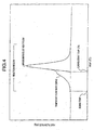
- Fig. 4 is a graph showing the relationship between temperature and calorific value as measured with a differential scanning calorimeter (DSC), which represents curing behavior of an adhesive.
- DSC differential scanning calorimeter
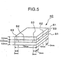
- Fig. 5 is a perspective view of a sample used to measure the saturation moisture absorption of the adhesive.
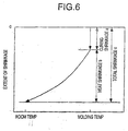
- Fig. 6 is a graph showing the relationship between the temperature and the extent of shrinkage of an organic insulating encapsulant.
- Figs. 3A to 3D show semiconductor device fabrication steps where a semiconductor element 1 is mounted on the semiconductor-mounting substrate.
- a semiconductor-mounting substrate 14 to be processed absorbs water content 12 as moisture from the atmosphere while it is left.
- a semiconductor element 1 is bonded to this substrate 14 via an adhesive 3 [Fig. 3B] and the device being in this step is heated in order to cure the adhesive 3
- the water content 12 adsorbed as moisture from the surface of the semiconductor-mounting substrate vaporizes as shown in Fig. 3C.
- This water content 12 may enter the adhesive 3 layer before the adhesive is begun to cure, so that voids 13 are formed in a large number as shown in Fig. 3D.
- the semiconductor device is fabricated using as it is the one having the voids 13 formed in the adhesive 3 layer
- water content separately absorbed as moisture and diffused from the back of the semiconductor-mounting substrate and from the organic insulating encapsulant 5 may easily be accumulated in the voids 13 of the adhesive 3 layer.
- the cracking or separation 11 comes to tend to occur as shown in Fig. 2.
- the present invention is based on such a new finding.
- Fig. 3A illustrates how the substrate 14 absorbs the water content 12 as moisture from the atmosphere while the semiconductor-mounting substrate 14 is left in the atmosphere.
- Fig. 3B is a cross-sectional view of the semiconductor-mounting substrate 14 on which the semiconductor element 1 has been mounted via the adhesive 3.
- Fig. 3C illustrates that the water content vaporizes from the surface of the semiconductor-mounting substrate 14 and enters the adhesive 3 layer while the substrate on which the element has been mounted, shown in Fig. 3B, is heated in an oven.
- Fig. 3D is a cross-sectional view showing that the voids 13 have been formed in the adhesive 3 layer after the heating step shown in Fig. 3C has been completed.
- the water content absorbed as moisture in the semiconductor-mounting substrate 14 comes to be the cause of forming the voids 13 in the adhesive 3 layer.
- the values of moisture absorption of a semiconductor-mounting substrate 14 commonly used in an atmosphere of 30°C and 60%RH are shown in Table 1.
- the semiconductor-mounting substrate 14 is a substrate comprising an insulating base material which is constituted of an epoxy resin and a glass cloth and on both sides of which fine wiring patterns are provided and are further covered thereon with an insulating protective resist.
- the semiconductor-mounting substrate used in BGA packaging begins to absorb moisture rapidly, and its moisture absorption reaches more than 0.1% by weight in few hours or so.
- the adhesive is applied and heated to cure in the same manner as that in conventional metallic-frame semiconductor devices (QFP and so forth), the water content vaporizes from the surface of the semiconductor-mounting substrate having absorbed as moisture the water content in the atmosphere, to enter the adhesive layer, and there is a possibility of causing voids in a large number.
- the curing start temperature of the adhesive is appropriately set so that the adhesive can be cured at a low temperature before the water content having vaporized from the surface of the semiconductor-mounting substrate enters the adhesive layer, and thus the adhesive layer can be prevented from causing voids.
- an adhesive having an exothermic-reaction curing start temperature (Th) of 130°C or below as measured with a differential scanning calorimeter (DSC) at a heating rate of 10°C/minute is used as the adhesive.
- the curing start temperature (Th) indicates, as shown in Fig. 4, the temperature in the part of a reaction region of a DSC temperature/heat flow rate curve and at which the curve starts to rise abruptly, immediately before it reaches the maximum rate of heat flow.
- the adhesive starts to react and cure abruptly, from the point of time it has reached this temperature.
- setting the Th to 130°C or below not only enables achievement of the effect of less causing the voids, but also promises a superior short-time curability, and hence this is very effective also for improving production efficiency.
- the adhesive used in the present invention may be of any types without any particular limitations as long as it has the curing performance described above.
- the adhesive may preferably be comprised of a base resin having a low viscosity and being of a solvent-free type.
- the base resin usable are acrylic resins, for example.
- an adhesive having a saturation moisture absorption of 0.18% or less under conditions of 30°C and 85%RH.
- the saturation moisture absorption is measured in the following way: As shown in Fig. 5, an adhesive 52 to be measured is put between two sheets of sheet glass 51 of 18 mm long, 18 mm wide and 0.2 mm thick and with flat surfaces, and four sheets of aluminum foil of 3 mm long, 3 mm wide and 0.03 mm thick are used as spacers 53. In Fig. 5, the scale in thickness direction is arbitrarily altered so as to be seen with ease.
- the mass (weight) of the sheet glass 51 and that of the aluminum foil (spacers 53) are accurately measured up to a figure of 0.01 mg.
- 50 to 60 mg of the adhesive 52 is put between the two sheets of sheet glass 51 together with the spacers 53, and then cured at 180°C for 1 hour.
- the mass of the resultant test piece is accurately measured up to a figure of 0.01 mg.
- the test piece is left to absorb moisture up to the lapse of 3,000 hours on which its mass comes to little change.
- the mass of the test piece after moisture absorption is accurately measured up to a figure of 0.01 mg.
- the saturation moisture absorption is a value SA calculated according to the following equation (1).
- SA ⁇ (V 2 - V 1 - V 0 )/(V 1 - V 0 ) ⁇ x 100
- the adhesive may preferably be those having an adhesive force as high as possible in order to prevent the adhesive from separating on the back of the semiconductor element or at the interface with the semiconductor-mounting substrate because of the vaporization and expansion of water content which are caused at the time of reflowing.
- those which do not greatly decrease in adhesive force as a result of moisture absorption are preferred.
- the present inventors made further detailed examination on a condition where the warpage deformation occurs in the semiconductor device, and have discovered that the warpage deformation can be made less occur when an encapsulant having specific properties is used as the organic insulating encapsulant 5. The effect of making this warpage deformation less occur is explained below.
- a shrinkage curve of an organic insulating encapsulant at temperatures of from molding temperature to room temperature is shown in Fig. 6.
- an organic insulating encapsulant is heated in a mold to effect curing and then released from the mold to leave it cool, first the organic insulating encapsulant reacts to cure at molding temperature.
- a shrinkage caused by the curing reaction hereinafter "curing shrinkage a.” occurs.
- a shrinkage based on linear expansion of the organic insulating encapsulant hereinafter "heat shrinkage b.” occurs.
- a shrinkage put together by adding the curing shrinkage a. and the heat shrinkage b. is total shrinkage c. of the organic insulating encapsulant.
- the organic insulating encapsulant is molded on a semiconductor device of one-side encapsulation structure like BGA and there is a great difference between the total shrinkage c. of the organic insulating encapsulant and the coefficient of linear expansion of the semiconductor element and semiconductor-mounting substrate which are adjoining thereto, a residual stress is produced in the interior of the semiconductor device to cause warpage deformation over the whole semiconductor device.
- the warpage deformation of laminated structures occurs as a result of accumulation of residual stress in the interior of the structures.
- it is effective to relax the residual stress in the interior of the semiconductor device.
- it is effective to lower the modulus of elasticity of constituent members.
- the organic insulating encapsulant it is effective for the organic insulating encapsulant to have a wide region of lowering of the modulus of elasticity in viscoelastic behavior within a temperature range of from room temperature to molding temperature, i.e., to have a glass transition temperature within this temperature range.
- the temperature region in which the modulus of elasticity of the organic insulating encapsulant lowers in a wide range is embraced in the temperature that is in the course of cooling to room temperature after package molding or in the course of raising temperature from room temperature in the step of solder reflowing.
- the residual stress produced in the device can be relaxed and the warpage deformation can effectively be made to less occur.
- the organic insulating encapsulant it is preferable to appropriately use as the organic insulating encapsulant an encapsulant having a glass transition temperature in the temperature range of from room temperature to molding temperature.
- the lower limit of the modulus of elasticity thus lowered may preferably be about 1/10 of the modulus of elasticity at room temperature.
- Molding temperature may preferably be within the range of from 170 to 180°C, but is not particularly limited thereto as long as it is within a temperature range in which the molding properties of the organic insulating encapsulant are not damaged.
- the substrate and the encapsulant may also be used in appropriate combination so that the semiconductor-mounting substrate and the organic insulating encapsulant may have a difference in heat shrinkage within a stated range. This enables relaxation of the residual stress to make small the warpage deformation on the level of semiconductor devices.
- the organic insulating encapsulant may preferably have a difference in coefficient of linear expansion, of 0.6 x 10 -5 /° C or above between the semiconductor-mounting substrate and the organic insulating encapsulant at a temperature not higher than the latter's glass transition temperature. This can effectively lower the extent of warpage deformation at the time of the cooling from molding temperature to room temperature.
- an organic insulating encapsulant having a specific value of extent of curing shrinkage at the time of molding can make small the warpage deformation on the level of semiconductor devices. Accordingly, in the present invention, it is preferable to use an organic insulating encapsulant having a curing shrinkage factor of 0.11% or less.
- An encapsulant which undergoes curing shrinkage at an appropriate extent not only can make the total shrinkage of the organic insulating encapsulant appropriate in extent against the warpage deformation caused when it is cooled from molding temperature to room temperature, but also can make the warpage deformation as small as possible at the temperature (in general, around molding temperature of about 170 - 180 ⁇ ⁇ ) at which the solder begins to melt at the time of solder reflowing, to contribute to an improvement in the reliability of connection with a substrate for mounting.
- the curing shrinkage factor is a value dP obtained in the following way: A test; piece constituted of a single member of 60.1 mm long, 6 mm wide and 1.5 mm thick is molded, and fist the molding cavity size in the longitudinal direction at molding temperature and the test piece size in the longitudinal direction at room temperature immediately after molding are accurately measured with a precision slide caliper up to a figure of 0.01 mm, and a shrinkage factor dL of the whole is calculated according to the following equation (2). Thereafter, a heat shrinkage factor dT at temperatures of from molding temperature to room temperature separately measured is subtracted from this value dL according to the following equation (3) to calculate the value dP.
- dL (L 0 - L)/L 0
- an organic insulating encapsulant having a saturation moisture absorption of 0.36% by weight or less at 85°C and 85%RH.
- the saturation moisture absorption is a value obtained in the following way: A disk (according to JIS-K6911) constituted of a single member of 50 mm diameter and 3 mm thick is dry-treated at 120°C for 2 hours as pretreatment, and then its mass (weight) is accurately measured up to a figure of 1 mg. Thereafter, in an atmosphere of 85°C and 85%RH, the test piece is left to absorb moisture up to the lapse of 3,000 hours on which its mass comes not to change any longer. The mass of the test piece after moisture absorption is accurately measured up to a figure of 1 mg.
- the organic insulating encapsulant may also preferably have a modulus in flexure of 4.0 GPa or below at a temperature at which the solder begins to melt, i.e., about the molding temperature.
- the modulus in flexure is a value obtained by making a three-point bending test on a test piece (according to JIS-K6911) constituted of a single member of 70 mm long, 10 mm wide and 3 mm thick, and calculated according to the following equation (5).
- E (I ⁇ P)/(4wh ⁇ y)
- the base resin of the organic insulating encapsulant those composed chiefly of an epoxy resin having a biphenyl skeleton are preferred in view of an advantage that the effect of especially great viscoelastic properties is obtainable within a temperature range of from molding temperature to room temperature.
- a material having a rigid structure that can make any free volumetric change small after curing may preferably be mixed for the purpose of reducing the curing shrinkage factor.
- a filler mixed in the organic insulating encapsulant may preferably be in an amount not less than 80% by volume in view of the controlling of heat shrinkage factor and moisture absorption.
- the insulating base material usable are, e.g., organic insulating base materials.
- Composite materials comprised of a reinforcing material such as glass cloth impregnated with a synthetic resin such as epoxy resin, polyimide or phenolic resin may be used, and besides synthetic resin films such as TAB (tape automated bonding) tape materials may be used.
- synthetic resin films such as TAB (tape automated bonding) tape materials may be used.
- TAB tape automated bonding tape materials
- those having a moisture absorption as low as possible may preferably be used so that any voids can be kept from being caused in the adhesive layer in the course of the curing of the adhesive and also the water content can be kept from being diffused from this base material member to the adhesive layer after the fabrication of semiconductor devices.
- a semiconductor-element-mounting substrate having an external size of 26.2 mm long, 26.2 mm wide and 0.6 mm thick having, as shown in Fig. 1, an insulating base material 2 (a glass cloth-epoxy resin laminated sheet available from Hitachi Chemical Co., Ltd.; trade name: E-679) on which fine wiring patterns 6 were formed and an insulating protective resist 4 (available from Taiyo Inki K.K.; trade name: PSR4000 AUS5) was coated on the surface except for gold-plated terminals 7 and opposite-side external connecting terminals 9, was dried at 120°C for 2 hours and then left for 5 hour in an atmosphere of 30°C and 60%RH.
- an insulating base material 2 a glass cloth-epoxy resin laminated sheet available from Hitachi Chemical Co., Ltd.; trade name: E-679
- an insulating protective resist 4 available from Taiyo Inki K.K.; trade name: PSR4000 AUS5
- a semiconductor element 1 of 9 mm long, 9 mm wide and 0.51 mm thick was mounted thereon, coating an adhesive 3 (available from Hitachi Chemical Co., Ltd.; trade name: EN-X50), followed by heating in an clean oven for 1 hour from room temperature to 180°C at a constant heating rate, and further followed by heating for 1 hour at a constant temperature of 180°C.
- an adhesive 3 available from Hitachi Chemical Co., Ltd.; trade name: EN-X50
- wire bonding portions and semiconductor element electrodes were wire-bonded through gold wires 8 of 30 ⁇ m in diameter.
- an organic insulating encapsulant 5 available from Hitachi Chemical Co., Ltd.; trade name: CEL-X9600
- the semiconductor element mounted area was encapsulated by transfer molding under conditions of 175 ⁇ ⁇ , 90 seconds, and 6.9 MPa, followed by post-curing under conditions of 175°C and 5 hours to obtain a BGA semiconductor device.
- a BGA semiconductor device was obtained in the same manner as in Example 1 except that a different adhesive (available from Hitachi Chemical Co., Ltd.; trade name: EN-X52) was used.
- a BGA semiconductor device was obtained in the same manner as in Example 1 except that CEL-9000 (trade name), available from Hitachi Chemical Co., Ltd., was used as the organic insulating encapsulant.
- CEL-9000 trade name
- the difference between the coefficient of linear expansion of the semiconductor-element-mounting substrate and the coefficient of linear expansion of the organic insulating encapsulant at a temperature not higher than the glass transition temperature is less than 0.6 x 10 -5 /°C.
- a BGA semiconductor device was obtained in the same manner as in Example 1 except that CEL-7700SX (trade name), available from Hitachi Chemical Co., Ltd., was used as the organic insulating encapsulant.
- the encapsulant used in the present Example had a curing shrinkage factor more than 0.11% and a saturation moisture absorption of more than 0.36% at 85° C and 85%RH.
- a BGA semiconductor device was obtained in the same manner as in Example 1 except that CEL-1731 (trade name), available from Hitachi Chemical Co., Ltd., was used as the organic insulating encapsulant.
- the encapsulant used in the present Example had a glass transition temperature at the molding temperature or above, where the difference between the coefficient of linear expansion of the semiconductor-element-mounting substrate and the coefficient of linear expansion of the organic insulating encapsulant at a temperature not higher than the glass transition temperature is less than 0.6 x 10 -5 /°C.
- the encapsulant had a modulus in flexure above 4.0 GPa at its molding temperature, and a saturation moisture absorption more than 0.36% at 85°C and 85%RH.
- a BGA semiconductor device was obtained in the same manner as in Example 1 except that an adhesive (available from Hitachi Chemical Co., Ltd.; trade name: EN-4570) having a saturation moisture absorption of 0.18% or more at 30°C and 85%RH was used as the adhesive.
- an adhesive available from Hitachi Chemical Co., Ltd.; trade name: EN-4570
- a BGA semiconductor device was obtained in the same manner as in Example 3 except that an adhesive (available from Hitachi Chemical Co., Ltd.; trade name: EN-4500) having a curing start temperature (Th) above 130°C was used as the adhesive.
- an adhesive available from Hitachi Chemical Co., Ltd.; trade name: EN-4500
- Thi curing start temperature
- the curing start temperature (Th) of the adhesive was measured with a differential scanning calorimeter (manufactured by TA Instruments Japan Inc.; trade name: Model 910) at a heating rate of 10° C/minute.
- the glass transition temperature of the organic insulating encapsulant was measured with a thermomechanical analyzer (manufactured by Rigaku International Corporation; trade name: TMA-8141BS, TAS-100).
- the semiconductor device was moistened for a stated time under conditions of 85°C and 60%RH, and thereafter reflow-treated three times at 240°C for 10 seconds in an infrared reflow furnace. Any voids and cracking or separation of the adhesive layer, having occurred in the interior of the semiconductor device were observed with an ultrasonic inspection device. Those in which the cracking or separation extended up to the gold-plated-terminal regions were regarded as defectives (number of defectives was written as a numerator, and number of test devices as a denominator).
- Examples 1 to 5 all did not cause any voids in their adhesive layers.
- Examples 1 to 3 showed a remarkable improvement in the resistance to reflow cracking.
- Comparative Example 1 making use of an adhesive having a high curing start temperature (Th), voids occurred in the adhesive layer.
- the present invention makes it possible to provide a semiconductor device that may less cause cracking at the time of solder reflowing. It also makes it possible to provide an OMPAC type BGA packaged semiconductor device that can prevent occurrence of warpage deformation. Hence, the use of the semiconductor device of the present invention enables reduction of faulty electrical connection, promising a great industrial value.
Landscapes
- Structures Or Materials For Encapsulating Or Coating Semiconductor Devices Or Solid State Devices (AREA)
- Die Bonding (AREA)
Applications Claiming Priority (5)
| Application Number | Priority Date | Filing Date | Title |
|---|---|---|---|
| JP21269698 | 1998-07-28 | ||
| JP21269798 | 1998-07-28 | ||
| JP21269798 | 1998-07-28 | ||
| JP21269698 | 1998-07-28 | ||
| PCT/JP1999/004016 WO2000007234A1 (fr) | 1998-07-28 | 1999-07-27 | Dispositif a semi-conducteur et procede de fabrication associe |
Publications (2)
| Publication Number | Publication Date |
|---|---|
| EP1111667A1 true EP1111667A1 (de) | 2001-06-27 |
| EP1111667A4 EP1111667A4 (de) | 2005-06-22 |
Family
ID=26519371
Family Applications (1)
| Application Number | Title | Priority Date | Filing Date |
|---|---|---|---|
| EP99931560A Withdrawn EP1111667A4 (de) | 1998-07-28 | 1999-07-27 | Halbleitervorrichtung und herstellungsverfahren |
Country Status (7)
| Country | Link |
|---|---|
| US (1) | US6611064B1 (de) |
| EP (1) | EP1111667A4 (de) |
| JP (1) | JP3916398B2 (de) |
| KR (1) | KR100418013B1 (de) |
| AU (1) | AU4802199A (de) |
| TW (1) | TW430908B (de) |
| WO (1) | WO2000007234A1 (de) |
Families Citing this family (8)
| Publication number | Priority date | Publication date | Assignee | Title |
|---|---|---|---|---|
| JP4752107B2 (ja) * | 2000-11-29 | 2011-08-17 | 日立化成工業株式会社 | 回路接続用フィルム状接着剤、回路端子の接続構造および回路端子の接続方法 |
| JP2004311784A (ja) * | 2003-04-08 | 2004-11-04 | Fuji Xerox Co Ltd | 光検出装置、及びその実装方法 |
| US20090273072A1 (en) * | 2005-03-31 | 2009-11-05 | Pioneer Corporation | Semiconductor device and method for manufacturing the same |
| KR100764164B1 (ko) * | 2006-04-04 | 2007-10-09 | 엘지전자 주식회사 | 인쇄회로기판과 이를 사용한 패키지 및 이들의 제조방법 |
| JP2009164500A (ja) * | 2008-01-10 | 2009-07-23 | Sumitomo Bakelite Co Ltd | 接着剤および半導体パッケージ |
| JP5625431B2 (ja) * | 2009-03-31 | 2014-11-19 | 住友ベークライト株式会社 | 半導体装置の製造方法 |
| KR101895183B1 (ko) | 2010-11-12 | 2018-09-04 | 에베 그룹 에. 탈너 게엠베하 | 웨이퍼 스택에 있는 결함 및 층 두께를 측정하기 위한 측정 장치 및 측정 방법 |
| US11688668B2 (en) * | 2019-12-31 | 2023-06-27 | At&S (China) Co. Ltd. | Component carrier with low shrinkage dielectric material |
Family Cites Families (31)
| Publication number | Priority date | Publication date | Assignee | Title |
|---|---|---|---|---|
| US3715589A (en) * | 1970-10-02 | 1973-02-06 | Matsushita Electric Industrial Co Ltd | Electromagnetic radiation image displaying panel |
| JPS57111034A (en) * | 1980-12-10 | 1982-07-10 | Hitachi Ltd | Semiconductor device and its manufacture |
| JPH0796618B2 (ja) * | 1986-11-20 | 1995-10-18 | 新日鐵化学株式会社 | 低熱膨張性樹脂 |
| JPH0721042B2 (ja) * | 1987-09-30 | 1995-03-08 | 三井石油化学工業株式会社 | 熱硬化性樹脂組成物 |
| US5300459A (en) * | 1989-12-28 | 1994-04-05 | Sanken Electric Co., Ltd. | Method for reducing thermal stress in an encapsulated integrated circuit package |
| US5173766A (en) * | 1990-06-25 | 1992-12-22 | Lsi Logic Corporation | Semiconductor device package and method of making such a package |
| US5134462A (en) * | 1990-08-27 | 1992-07-28 | Motorola, Inc. | Flexible film chip carrier having a flexible film substrate and means for maintaining planarity of the substrate |
| US5122858A (en) * | 1990-09-10 | 1992-06-16 | Olin Corporation | Lead frame having polymer coated surface portions |
| US5250600A (en) * | 1992-05-28 | 1993-10-05 | Johnson Matthey Inc. | Low temperature flexible die attach adhesive and articles using same |
| JPH06103707B2 (ja) * | 1991-12-26 | 1994-12-14 | インターナショナル・ビジネス・マシーンズ・コーポレイション | 半導体チップの交換方法 |
| US5313365A (en) * | 1992-06-30 | 1994-05-17 | Motorola, Inc. | Encapsulated electronic package |
| US5703405A (en) * | 1993-03-15 | 1997-12-30 | Motorola, Inc. | Integrated circuit chip formed from processing two opposing surfaces of a wafer |
| US5667884A (en) * | 1993-04-12 | 1997-09-16 | Bolger; Justin C. | Area bonding conductive adhesive preforms |
| US5767580A (en) * | 1993-04-30 | 1998-06-16 | Lsi Logic Corporation | Systems having shaped, self-aligning micro-bump structures |
| DE69426347T2 (de) * | 1993-09-29 | 2001-05-17 | Matsushita Electric Industrial Co., Ltd. | Verfahren zum Montieren einer Halbleiteranordnung auf einer Schaltungsplatte und eine Schaltungsplatte mit einer Halbleiteranordnung darauf |
| US5734201A (en) * | 1993-11-09 | 1998-03-31 | Motorola, Inc. | Low profile semiconductor device with like-sized chip and mounting substrate |
| US5473512A (en) * | 1993-12-16 | 1995-12-05 | At&T Corp. | Electronic device package having electronic device boonded, at a localized region thereof, to circuit board |
| US5504374A (en) * | 1994-02-14 | 1996-04-02 | Lsi Logic Corporation | Microcircuit package assembly utilizing large size die and low temperature curing organic die attach material |
| JPH07247364A (ja) * | 1994-03-10 | 1995-09-26 | Toyota Central Res & Dev Lab Inc | オリゴマー分解性高分子、その製造方法、回収方法及び再生方法 |
| JP3200280B2 (ja) * | 1994-03-30 | 2001-08-20 | シャープ株式会社 | 半導体装置の製造方法 |
| FR2723257B1 (fr) * | 1994-07-26 | 1997-01-24 | Sgs Thomson Microelectronics | Boitier bga de circuit integre |
| JP3406073B2 (ja) | 1994-08-12 | 2003-05-12 | 日立化成工業株式会社 | 樹脂封止型半導体装置 |
| US5508556A (en) * | 1994-09-02 | 1996-04-16 | Motorola, Inc. | Leaded semiconductor device having accessible power supply pad terminals |
| US5741446A (en) * | 1995-05-26 | 1998-04-21 | Mitsubishi Engineering-Plastics Corp. | Method of producing a molded article using a mold assembly with an insert block |
| TW310481B (de) * | 1995-07-06 | 1997-07-11 | Hitachi Chemical Co Ltd | |
| US6717242B2 (en) * | 1995-07-06 | 2004-04-06 | Hitachi Chemical Company, Ltd. | Semiconductor device and process for fabrication thereof |
| US6242802B1 (en) * | 1995-07-17 | 2001-06-05 | Motorola, Inc. | Moisture enhanced ball grid array package |
| TW334469B (en) * | 1995-08-04 | 1998-06-21 | Doconitele Silicon Kk | Curable organosiloxane compositions and semiconductor devices |
| JP3377660B2 (ja) * | 1995-09-29 | 2003-02-17 | シャープ株式会社 | 加熱炉およびダイボンドペーストの硬化方法 |
| US5773895A (en) * | 1996-04-03 | 1998-06-30 | Intel Corporation | Anchor provisions to prevent mold delamination in an overmolded plastic array package |
| US5783866A (en) * | 1996-05-17 | 1998-07-21 | National Semiconductor Corporation | Low cost ball grid array device and method of manufacture thereof |
-
1999
- 1999-07-27 JP JP2000562946A patent/JP3916398B2/ja not_active Expired - Lifetime
- 1999-07-27 WO PCT/JP1999/004016 patent/WO2000007234A1/ja not_active Ceased
- 1999-07-27 KR KR10-2001-7001186A patent/KR100418013B1/ko not_active Expired - Fee Related
- 1999-07-27 US US09/744,577 patent/US6611064B1/en not_active Expired - Fee Related
- 1999-07-27 AU AU48021/99A patent/AU4802199A/en not_active Abandoned
- 1999-07-27 EP EP99931560A patent/EP1111667A4/de not_active Withdrawn
- 1999-07-28 TW TW088112815A patent/TW430908B/zh not_active IP Right Cessation
Also Published As
| Publication number | Publication date |
|---|---|
| JP3916398B2 (ja) | 2007-05-16 |
| US6611064B1 (en) | 2003-08-26 |
| AU4802199A (en) | 2000-02-21 |
| KR20010071046A (ko) | 2001-07-28 |
| EP1111667A4 (de) | 2005-06-22 |
| KR100418013B1 (ko) | 2004-02-14 |
| TW430908B (en) | 2001-04-21 |
| WO2000007234A1 (fr) | 2000-02-10 |
Similar Documents
| Publication | Publication Date | Title |
|---|---|---|
| US5937279A (en) | Semiconductor device, and manufacturing method of the same | |
| US6236108B1 (en) | Substrate for holding a chip of semi-conductor package, semi-conductor package, and fabrication process of semi-conductor package | |
| JP3648277B2 (ja) | 半導体装置 | |
| US7141874B2 (en) | Electronic component packaging structure and method for producing the same | |
| US7378731B2 (en) | Heat spreader and package structure utilizing the same | |
| US5838061A (en) | Semiconductor package including a semiconductor chip adhesively bonded thereto | |
| US7180007B2 (en) | Electronic circuit device and its manufacturing method | |
| JP3134815B2 (ja) | 半導体装置 | |
| WO2004043130A2 (en) | Mechanically enhanced package and method of making same | |
| JPH11150135A (ja) | 熱伝導性が良好な導電性ペースト及び電子部品 | |
| US6611064B1 (en) | Semiconductor device and method for manufacturing the same | |
| US7344916B2 (en) | Package for a semiconductor device | |
| KR100295731B1 (ko) | 전자패키지의제조방법 | |
| JPWO2000007234A1 (ja) | 半導体装置およびその製造方法 | |
| US5877553A (en) | Metallic electronic component packaging arrangement | |
| JPH1171444A (ja) | エポキシ樹脂組成物及び半導体装置 | |
| WO2004030075A1 (ja) | 半導体装置の製造方法 | |
| JP2970548B2 (ja) | 半導体装置 | |
| Nakagawa et al. | High density packaging technology ultra thin package & new TAB package | |
| Yoshida et al. | An extremely thin BGA format chip-scale package and its board level reliability | |
| JP3951903B2 (ja) | 半導体装置及び半導体装置実装体の製造方法 | |
| JPH0680701B2 (ja) | ピン付チツプキヤリア | |
| Koh et al. | Low stress encapsulants for reduced failures in plastic packages | |
| CN120237116A (zh) | 球栅阵列封装 | |
| WO2024154790A1 (ja) | 配線基板、電気装置および電気装置構造体 |
Legal Events
| Date | Code | Title | Description |
|---|---|---|---|
| PUAI | Public reference made under article 153(3) epc to a published international application that has entered the european phase |
Free format text: ORIGINAL CODE: 0009012 |
|
| 17P | Request for examination filed |
Effective date: 20010130 |
|
| AK | Designated contracting states |
Kind code of ref document: A1 Designated state(s): AT BE CH CY DE DK ES FI FR GB GR IE IT LI LU MC NL PT SE |
|
| D18D | Application deemed to be withdrawn (deleted) | ||
| A4 | Supplementary search report drawn up and despatched |
Effective date: 20050506 |
|
| RIC1 | Information provided on ipc code assigned before grant |
Ipc: 7H 01L 21/58 B Ipc: 7H 01L 23/31 B Ipc: 7H 01L 21/52 A |
|
| STAA | Information on the status of an ep patent application or granted ep patent |
Free format text: STATUS: THE APPLICATION IS DEEMED TO BE WITHDRAWN |
|
| 18D | Application deemed to be withdrawn |
Effective date: 20070719 |