EP0634796A1 - Bipolartransistor mit isoliertem Gate - Google Patents
Bipolartransistor mit isoliertem Gate Download PDFInfo
- Publication number
- EP0634796A1 EP0634796A1 EP94110811A EP94110811A EP0634796A1 EP 0634796 A1 EP0634796 A1 EP 0634796A1 EP 94110811 A EP94110811 A EP 94110811A EP 94110811 A EP94110811 A EP 94110811A EP 0634796 A1 EP0634796 A1 EP 0634796A1
- Authority
- EP
- European Patent Office
- Prior art keywords
- region
- type
- collector region
- collector
- base region
- Prior art date
- Legal status (The legal status is an assumption and is not a legal conclusion. Google has not performed a legal analysis and makes no representation as to the accuracy of the status listed.)
- Granted
Links
Images




Classifications
-
- H—ELECTRICITY
- H10—SEMICONDUCTOR DEVICES; ELECTRIC SOLID-STATE DEVICES NOT OTHERWISE PROVIDED FOR
- H10D—INORGANIC ELECTRIC SEMICONDUCTOR DEVICES
- H10D12/00—Bipolar devices controlled by the field effect, e.g. insulated-gate bipolar transistors [IGBT]
- H10D12/411—Insulated-gate bipolar transistors [IGBT]
- H10D12/441—Vertical IGBTs
-
- H—ELECTRICITY
- H10—SEMICONDUCTOR DEVICES; ELECTRIC SOLID-STATE DEVICES NOT OTHERWISE PROVIDED FOR
- H10D—INORGANIC ELECTRIC SEMICONDUCTOR DEVICES
- H10D62/00—Semiconductor bodies, or regions thereof, of devices having potential barriers
- H10D62/10—Shapes, relative sizes or dispositions of the regions of the semiconductor bodies; Shapes of the semiconductor bodies
- H10D62/13—Semiconductor regions connected to electrodes carrying current to be rectified, amplified or switched, e.g. source or drain regions
- H10D62/141—Anode or cathode regions of thyristors; Collector or emitter regions of gated bipolar-mode devices, e.g. of IGBTs
- H10D62/142—Anode regions of thyristors or collector regions of gated bipolar-mode devices
Definitions
- the present invention relates to a semiconductor power device, and particularly to an Insulated Gate Bipolar Transistor (hereinafter, referred to as an IGBT) being a MOS Bipolar composite functional device capable of performing high-speed operations in a medium electric power area of breakdown voltage 1200V or more.
- IGBT Insulated Gate Bipolar Transistor
- MOS composite devices such as an IGBT, a MOS Controlled Thyristor (MCT), an Emitter Switched Thyristor (EST), or the like have been developed. Since these are voltage-driving power devices and easy to use, requirements for developing these new MOS composite devices have fairly been made from a system operation side and its development has abruptly been advanced in response thereto.
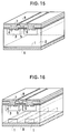
- the IGBT is a transistor having a unit cell cross-sectional structure as represented in Fig. 13, and has a composite structure provided with a MOSFET structure in its upper part and a bipolar transistor structure in its lower part.
- This structure and basic operations are disclosed in the Japanese Patent Application Laid Open No. 57-120369 Official Gazette.
- a conventional N-channel IGBT will be explained.
- a high-resistivity N ⁇ base region 2 having low impurity concentration is formed in a P-type collector region 1.
- a P-type base region 3 is formed by a Double Diffusion Self Alignment method so as to expose its surface.
- an N+ emitter region 4 is formed in the P-type base region 3 so as to expose its surface.
- a polysilicon gate electrode 6 is provided on a thin insulation film 5 such as SiO2 etc. This gate electrode 6 steps over the P-type base region 3 and is disposed so as to cover from the N ⁇ base region 2 to the N+ emitter region 4.
- a metal emitter electrode 7 is provided so that the N+ emitter region 4 may be short-circuited with the P-type base region 3, and a metal gate 8 connecting to the polysilicon gate electrode 6 and a metal collector electrode 9 connecting to the P-type collector region 1 are provided, respectively. Also, in a structure as depicted in Fig.
- an N+ buffer region 20 is provided between the P-type collector region 1 and N ⁇ base region 2 and such IGBT has generally been known.
- a general method of manufacturing these conventional N-channel IGBTs will be described below.
- the P-type silicon semiconductor substrate 1 having a thickness of about 150 ⁇ m and impurity concentration of about 1018 to 1020 cm ⁇ 3 is used as a P-type collector region.
- a semiconductor layer 2 is formed in vapor-phase epitaxy on this semiconductor substrate 1 to act as the N ⁇ base region.
- the semiconductor layer 2 will be formed.
- a P-N ⁇ (or P-N-N ⁇ ) wafer is formed.
- the insulation film 5 such as SiO2 etc. is formed on the surface of the N ⁇ base region 2, and further the polysilicon gate electrode 6 is formed thereon.
- the polysilicon gate electrode 6 and insulation film 5 are partially opened, and with the use of the polysilicon electrode 6 as a mask, the P-type base region 3 is formed, and further two N+ emitter regions 4 are formed within the P-type base region 3.
- the insulation film 5 is formed again on the polysilicon gate electrode 6 and P-type base region 3, and further the insulation film 5 formed on the P-type base region 3 containing the polysilicon gate electrode 6 and N+ emitter region 4 is partially removed.
- N+ emitter region 4 and the polysilicon gate electrode 6 are deposited with a metal such as aluminum etc. to form the metal gate electrode 8 and metal emitter electrode 7.
- the metal collector electrode 9 is formed in the P-type collector region 1 to obtain the conventional IGBT as shown in Figs. 13, 14.
- the metal emitter electrode 7 is connected to the ground and a positive voltage for the metal emitter electrode 7 is applied to the metal gate electrode 8 in a condition that a positive voltage is applied to the metal collector electrode 9, whereby a turn-on of the IGBT can be realized.
- a positive voltage is applied to the metal gate electrode 8
- an inversion channel is formed on the surface of the P-type base region 3 in the same manner as the MOSFET and electrons flow into the inside of the N ⁇ base region 2 through the inversion channel from the N+ emitter region 4.
- a negative voltage for the metal emitter electrode 7 is applied to the metal gate electrode 8, whereby a turn-off of the IGBT can be realized.
- the inversion channel is vanished and electrons stop flowing into the N ⁇ base region 2 from the N+ emitter region 4.
- electrons have existed as before within the N ⁇ base region 2.
- Most of holes stored within the N ⁇ base region 2 pass through the P-type base region 3 and flow into the emitter electrode 7, however a part thereof is recombined with electrons existing within the N ⁇ base region 2 and disappears.
- the IGBT becomes in a blocking state to complete the turn-off.
- the high-voltage IGBT is an excellent element showing extremely low on-resistance, however there are some drawbacks that, since it is a minority carrier device, a turn-off time is elongated. A part of a minority carriers (holes) which are injected from a collector region to an N ⁇ base region is stored within the N ⁇ base region as excessive minority carriers. Accordingly, even if a gate voltage is reduced to zero in order to turn off this IGBT and the channel is closed to stop a flow of electrons, an off-state is not available until the stored minority carriers have been discharged.
- a method of improving the turn-off time of the IGBT a method of shortening a carrier life time is generally adopted in the prior art. Specifically, a heavy metal diffusion method such as Au, Pt is taken, or the carrier life time is shortened by radioactive ray such as neutron rays, ⁇ rays or electron beams. Although the turn-off time is improved in this method, the degree of conduction modulation in the N ⁇ base region is simultaneously lowered and the low on-resistance characteristic which is the maximum advantage of the IGBT is deteriorated. Also, as another method, there is a method that the injection of holes from the P-type collector region is suppressed reducing the impurity concentration in the P-type collector region. With reference to Fig.
- the axis of ordinates denotes a turn-off time ( ⁇ s) and the axis of abscissas denotes total impurity dose Q D in the case where it is estimated per 1 cm2 of the entire area of a unit cell D in a collector region of IGBT.
- a curve as shown in this diagram is the characteristics of IGBT in which the collector region with a depth of 0.1 ⁇ m is formed on the entire surface of a second main surface of a semiconductor substrate and further a carrier life time shortening is employed to obtain the turn-off time of 10 ⁇ s.
- a numerical value Cs on the curve denotes impurity concentration in the collector region.
- the total impurity dose in the collector region on the axis of abscissas is a vale when ions of 11B+ are implanted at 20KeV through an oxide film having a film thickness 100nm. From a viewpoint of Fig. 12, it is understood, as one method of improving the turn-off time, that it is necessary to reduce the impurity concentration in the collector region in order to suppress injection efficiency of holes from the collector region.
- the impurity concentration in the P-type collector region is reduced, the contact resistance between the semiconductor collector region and metal collector electrode is increased and its amount of scatter are also extended, whereby this poor contact deteriorates the on-resistance characteristics of the IGBT.
- junction depth should be shallow, or 0.1 ⁇ m, with such a low total impurity dose in collector region 1 of about 1012 to 1014 cm ⁇ 2, to obtain high surface impurity concentration required to make a good ohmic contact. And if the junction depth is shallowed like this, the metal material of collector electrode penetrates through the collector region to produce a spike or a piping. Then, it is apprehensive that the N ⁇ base region is short-circuited and it is difficult to stably manufacture the device.
- a thick N ⁇ base region having very low concentration of 5X10¹³ atm/cm3 or less and a thickness of 100 ⁇ m or more is required, and it is difficult to form such thick epitaxial layer or to stably manufacture devices by the present vapor-phase epitaxy.
- a double diffusion type DMOS structure is formed on one main surface of an N ⁇ semiconductor substrate having low concentration and the P-type collector region 1 is formed on the other main surface by implanting ions, and such structure has been disclosed in the Japanese Patent Application Laid Open No. 2-7569 Official Gazette.
- the junction must be shallowed, or 0.1 ⁇ m to make an ohmic contact with the metal collector electrode 9, and then it is apprehensive that the metal collector electrode penetrate through the P+ collector region 1 and that the P+ collector region 1 is short-circuited with the N ⁇ base region 2, therefore there occur some problems that it is impossible to manufacture stably devices.
- the P-type collector region 1 is partially provided and the metal collector electrode 9 is formed so that the P-type collector region 1 may be short-circuited with the N ⁇ base region 2.
- the corrector-short IGBT IGBT as shown in Fig. 16
- the P-type collector region 1 is partially provided and the metal collector electrode 9 is formed so that the P-type collector region 1 may be short-circuited with the N ⁇ base region 2.
- IGBT new semiconductor device
- a semiconductor device of the present invention is an IGBT characterized in that a collector region is partially formed on the specific main surface of a semiconductor substrate, and in that a collector electrode is electrically connected with only the collector region in the semiconductor substrate. That is, the semiconductor device of the present invention is characterized by providing a semiconductor substrate, a first conductivity type (for example, N-type) base region formed on the semiconductor substrate and exposing onto a first main surface of the semiconductor substrate, a second conductivity type (P-type) base region formed within the N-type base region and exposing onto the first main surface of the semiconductor substrate, an N-type emitter region formed within the P-type base region and exposing onto the first main surface of the semiconductor substrate.
- a first conductivity type for example, N-type
- P-type second conductivity type
- a gate insulation film stepping over the emitter region and the N-type base region on the first main surface and formed on the P-type base region. And a gate electrode formed on the gate insulation film, an emitter electrode formed so as to step over the emitter region and the P-type base region on the first main surface and short-circuiting between this emitter region and the P-type base region.
- a P-type collector region formed partially on the second main surface of the semiconductor substrate, and a collector electrode connecting electrically in the window part of the collector region in the semiconductor substrate.
- An insulation film is formed on the second main surface excluding the window part of the collector region, and the collector electrode extends on this insulation film.
- the collector region may be disposed right under the gate electrode, or right under the emitter region or right under the gate electrode and the emitter region.
- a junction depth of the P-type collector region is decided by heat treatment conditions, and when the total impurity dose and junction depth in the collector region are made constant, its surface concentration is decided by an area of the P-type collector region for the entire area on the reverse surface of the IGBT forming the collector electrode, and the smaller its area becomes, the higher the surface concentration can be set.
- Fig. 1 is a perspective view of a semiconductor device of the present invention
- Fig. 2 is a plane view showing a first main surface of a semiconductor substrate 2 omitting an insulation film 5, a polysilicon gate 6, or the like of Fig. 1.
- D of Fig. 2 denotes a unit cell, and actually a plurality of unit cells are disposed in accordance with a desired current.
- This embodiment is explained using an N-channel transistor, however the present invention can be applied to a P-channel transistor irrespective of a channel type.
- a high resistiviy N-type silicon semiconductor substrate having (100) surface acting as N ⁇ base region 2 is prepared, and a P-type collector region 1 is formed on its second main surface.
- a P-type base region 3 is formed so that its surface may be exposed onto the surface of the N ⁇ base region 2, that is onto the first main surface of the silicon semiconductor substrate.
- an N+ emitter region 4 is formed so that its surface may be exposed onto the P-type base region 3.
- a polysilicon gate 6 is provided on a thin gate insulation film 5 such as SiO2 etc. on the surface of the P-type base region 3.
- a refractory metal such as W, Ti, Mo, or their silicides, or their polycides may be used instead of polysilicon.
- This polysilicon gate 6 steps over the P-type base region 3 and is disposed so as to cover from the N- base region 2 to the N+ emitter region 4.
- a metal emitter electrode 7 such as Al, Al-Si, Al-Cu-Si is provided so that the N+ emitter region 4 can be short-circuited with the P-type base region 3 on the surface, and a metal gate electrode 8 such as Al etc. connecting to the polysilicon gate 6 and a metal collector electrode 9 such as Al, Al-Si, Al-Cu-Si, Au, W, Mo connecting to the P-type collector region 1 are provided, respectively.
- the first embodiment of the present invention is characterized in not that the P-type collector region 1 is formed on the entire surface of a second main surface of the semiconductor substrate 2, in but that the P-type collector region 1 is partially formed.
- the P-type collector region 1 is disposed right under and along the gate 6.
- a collector electrode 9 is electrically connected with the P-type collector region 1 in the contact window on the surface of the semiconductor substrate 2. Accordingly, as the collector electrode 9 is formed on the entire surface of the second main surface, in order to prevent a contact with other regions, regions other than the contact window of P-type collector region 1 are coated with an insulation film 10.
- the collector electrode 9 coats the insulation film 10 and the P-type collector region 1, and this insulation film 10 may extend so as to partially coat the P-type collector region 1.
- SiO2 is used as its material in this embodiment.
- a material in the present invention is not limited to this one and Si3N4, Al2O3, SiO2/Si3N4, SiO x N y , SiO3N4/SiO2, SiO2/Si3N4/SiO2, Si3N4/SiO2/Si3N4, or oxygen-doped polycrystalline-silicon film (SIPOS) can also be used.
- SIPOS oxygen-doped polycrystalline-silicon film
- an N-type silicon semiconductor substrate 2 (N ⁇ base region) having resistivity 20 ⁇ cm or more and a thickness about 250 ⁇ m is prepared, and the entire surface of this N ⁇ base region 2 is thermally oxidized to form a field oxide film of 0.8 to 1.5 ⁇ . Thereafter the field oxide film in a part in which a device region will be formed is removed thermally oxidize again the exposed Si surface to form the gate insulation film 5 of about 100nm.
- the polysilicon gate 6 of 500nm is deposited thereon by a Chemical Vapor Deposition (CVD) method etc. Thereafter, the polysilicon gate 6 is cut and formed using photolithography technology and RIE etc.
- an oxide film is formed by the CVD method etc. on the surface of the P-type base region 3 and thereafter an oxide film mask (not shown) having an window for forming the emitter region 4 is formed by the photolithography, and with the use of this oxide film mask and the polysilicon gate 6 as a mask, 75A S + ions of the dose 5X1015cm-2 are implanted, and after heat treatment, the N+ emitter region 4 is formed within the P-type base region 3.
- insulation films 5, 10 of about 0.8 - 1.5 ⁇ m are formed on the entire surface of the first and second main surfaces of the semiconductor substrate 2 by the CVD method. Thereafter, after the insulation film 10 on the back surface (second main surface) of the N ⁇ base region 2 is partially removed, ions of boron (11B+, 49BF2+) of the dose 1X1012cm ⁇ 2 to 1X1014cm ⁇ 2 are implanted from the window part. Thereafter, after heat treatment, the P-type collector region 1 is formed in depth about 3 to 10 ⁇ m from the back surface. When the collector region 1 is formed in depth about 10 ⁇ m, before a process of forming the gate oxide film 5 on the first main plane surface, the process of forming the collector region is beforehand carried out.
- the insulation films 5, 10 on the first and second main surfaces are selectively removed, and after a metal such as Al, Al-Si has been formed on the entire surface of the first main surface, it is patterned to form the metal emitter electrode 7 and metal gate electrode 8.
- a metal such as Al, Au, Au-Sb, Mo, W is deposited on the second main surface to form the metal collector electrode 9, so that the semiconductor device as shown in Fig. 1 can be completed.
- the P-type collector region 1 formed on the second main surface (back surface) is partially formed, and the metal collector electrode 9 comes into contact with only the P-type collector region 1 in the window part of the back surface, whereby, even if the total impurity dose taking into consideration of the entire area of the substrate surface is set low at about 1012 to 1014 cm ⁇ 2, substantial impurity density in the P-type collector region 1 can be made high. Therefore, as the junction depth of the P-type collector region 1 can be deeper and surface concentration can be higher, the metal collector electrode 9 could not penetrate through the P-type collector region 1 (so-called piping) unlike the conventional structure shown in Fig. 15.
- the P-type collector region 1 is short-circuited with the N ⁇ base region 2. Also, as an alloy temperature for forming an ohmic contact of the collector electrode can be sufficiently made high, the P-type collector region 1 is connected stably with the metal collector electrode 9, the attempts to reduce ohmic resistance, improve an on-voltage, and manufacture stably devices are easily made.
- the junction depth of the P-type collector region 1 can be set at a desired depth according to heat treatment conditions, however when the total impurity amount and junction depth are made constant, the surface density comes to depend on a ratio of the surface area of the P-type collector region or a contact window area to the entire cell area, and the more its area is reduced, the higher the surface concentration can be made.
- the area is extremely made small, as the contact window area with the metal collector electrode 9 becomes small, the contact resistance is increased and the increased resistance exerts bad influences on the on-voltage. As a result, it is not favorable that the area of the collector region is reduced so that its area may become 1/25 times or less to the area of the unit cell D shown in Fig. 2.
- the high impurity concentration P++-type layer is rediffused only on the surface of the collector region in depth 50 to 100nm.
- the metal collector electrode 9 may be formed on the rediffused P++-type layer by vacuum-evaporation, sputtering, a CVD method, or the like. More specifically, 49BF2+ of the dose 5X1015 cm ⁇ 2 is implanted at 60keV and annealed at 800°C for about 30 min., or a thin film of boron is directly formed by the CVD method such as Molecular Layer Doping (MLD) etc., namely these methods are effective.
- MLD Molecular Layer Doping
- the total impurity amount in the P-type collector region 1 can be set at an extremely low value, or at less than 1012 cm ⁇ 2, a carrier life time in the N ⁇ base region 2 keeps long, while the hole injection from the P-type collector region 1 is suppressed to be extremely low, whereby a very high-speed turn-off characteristic can be obtained.
- the carrier life time in the N ⁇ base region 2 is prolonged and density in a recombination center is low, the holes injected from the P-type collector region 1 are contributed to conductivity modulation with excellent efficiency and the on-voltage becomes low and the trade-off relationship between the on-voltage (V CE (sat)) and turn-off time (t f ) can considerably be improved and a trade-off curve is shifted to the low on-voltage and high-speed turn-off side.
- a carrier life time killer can be formed only in the N ⁇ base region 2 in an intermediate part in the P-type collector regions 1 corresponding respectively to the adjoining unit cells D. If the life time killer is selectively formed like this, a turn-off time can be shortened without reducing the degree of the conductivity modulation in the region in which a main current flows.
- collector short structure in which an n+ region is formed on the second main surface in the N ⁇ base region 2 in an intermediate part of the adjoining P-type collector regions 1, the more high-speed turn-off is available by extracting electrons.
- an interval of the adjoining P-type collector regions 1, that is a pitch of the unit cell D is picked out so as to be about two times or less as much as a diffusion length L n of electrons, the electrons are effectively extracted, so that the turn-off with extremely few tail current can be realized.
- FIG. 3 to 7 are perspective views of a semiconductor device (IGBT) which has the same structure as Fig. 1 excluding a P-type collector region as shown in the figures.
- the P-type collector region 1 is formed parallel to the P-type base region 3, and as the region 1 is formed right under and along the polysilicon gate 6 disposed in a stripe form, its MOS characteristic can be enhanced.
- the P-type collector region 1 is formed parallel to the P-type base region 3 right under and along this P-type base region 3. Accordingly, two collector regions of this type are disposed in a stripe form in one cell region of IGBT. With such structure, a bipolar characteristic is enhanced by forming a PNP structure vertically.
- the P-type collector region 1 is formed in a stripe form and disposed in the direction of crossing perpendicularly the polysilicon gate 5 and the P-type base region 3. Therefore, the P-type collector region 1 is formed right under the polysilicon gate 6 and P-type base region 3. Accordingly, the MOS characteristic and bipolar characteristic are improved.
- the P-type collector region 1 is formed parallel to the P-type base region 3 right under and along this P-type base region 3 and the polysilicon gate 6. Accordingly, three collector regions of this type are disposed in a stripe form in one cell region of IGBT. With such structure, the MOS characteristic and bipolar characteristic are improved.
- the P-type collector region 1 is formed in a stripe form in the same manner as Fig. 4 and disposed in the direction of about 45 degrees with respect to the polysilicon gate 5 and P-type base region 3. Therefore, as the P-type collector region 1 is formed right under the polysilicon gate 6 and P-type base region 3, the MOS characteristic and bipolar characteristic are ameliorated. Wen using such a substrate that (111) surface is main plane surface, as an N ⁇ base region, it is also effective that the region is disposed in the direction of 60 degrees from crystal symmetry. In any of these embodiments, the same effects as the IGBT of Fig. 1 can be obtained. As long as the total impurity and area in the P-type collector region 1 and the contact window area with the collector electrode 9 are same, no differences in the device characteristics appear even in any embodiments.
- Figs. 1 to 7 depict such an embodiment that an upper MOSFET region in the IGBT has a stripe structure, however the present invention can also, of course, be applicable to such an embodiment that the MOSFET region has a mesh structure.
- Fig. 8 is a plane view of a first main surface of a semiconductor substrate in order to define the position relationship between the P-type collector region and P-type base region of the IGBT of Fig. 1.
- a plurality of P-type base regions 3 are substantially spaced and arranged in a stripe form within the semiconductor substrate 2.
- the P-type collector region 1 is formed right under between the adjoining two P-type collector regions 3 having a stripe form in the same manner.
- This polysilicon gate of the IGBT (not shown) is formed right under the P-type collector region 1 and formed on the first main surface of the semiconductor substrate 2 so as to step over two P-type base regions 3.
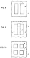
- Figs. 9 to 11 show a P-type base/P-type collector structure other than Figs. 3 to 7.
- the P-type collector region 1 is a regular square and formed at substantially constant intervals right under between the P-type base regions 3 disposed parallel in a stripe form in the same manner as Fig. 8.
- the polysilicon gate has the different shape from the P-type collector region 1 and is continuously linked together and formed on the first main surface so as to step over the P-type base region 3 right above the P-type collector region 1.
- the P-type base regions 3 are substantially a regular square and arranged on the first main surface in a matrix form.
- the P-type collector region 1 is formed right under between the P-type base regions 3.
- four P-type base regions 3 are shown and a cross of P-type collector region 1 is disposed.
- the polysilicon gate is continuously formed between these P-type base regions 3 and latticed. This collector region is continuously formed in a lattice form with neighboring unit cells.
- four P-type base regions 3 are shown and four P-type collector regions 1 are disposed. In such a manner, the shape of the P-type collector region 1 is not exceptionally limited.
- the turn-off time t f depends on the total impurity dose Q D in the collector region, and when this impurity dose is suppressed to be about 1014 atm/cm2 or less, the turn-off time t f can be made about 1.5 ⁇ s or less.
- the embodiment of the present invention maintains this low total impurity dose, while the collector region 1 is locally limited without forming it on the entire surface and the contact window area in the collector region coming into contact with the metal collector electrode is relatively made smaller, whereby substantial impurity concentration in the collector region 1 can be increased.
- the junction depth can be made deeper than usual (about 0.1 ⁇ m), and as a result, the metal collector electrode does not penetrate through the collector region and it is possible to stably carry out the junction and to stably manufacture devices.
- the collector region is shallow, or in about 0.1 ⁇ m, as its metal semiconductor interface is silicified and short-circuited with a base region by the phenomenon such as an Al-spike, an Al-piping, hole injection efficiency etc. are deteriorated.
- the junction depth in the present invention is deep, or in 3 to 10 ⁇ m, such problems never occur, and reversely it becomes possible to increase a heat treatment temperature for forming an ohmic contact electrode.
- the semiconductor substrate of the present invention does not need a semiconductor layer formation by a vapor-phase epitaxy therein, semiconductor devices can stably and readily be fabricated. Nevertheless, the present invention can be applied to semiconductor devices containing a conventional buffer layer as shown in Fig. 14.
- the antinomic relation that the requirement to decrease the impurity concentration for lowering the collector injection efficiency and that to increase the impurity concentration for making favorable an ohmic contact must be satisfied at the same time. Therefore, according to the present invention, it is possible to simultaneously reduce two parameters such as a reduction in a turn-off time t f and a reduction in an on-voltage V CE (sat) which has the trade-off relations each other. Consequently, a trade-off curve of the turn-off time t f and the on-voltage V CE (sat) is shifted to the side of a high-speed turn-off and a low on-voltage. Moreover, a manufacturing process for executing this is extremely simple and stable and a manufacturing yield becomes high.
- boron of the P-type impurity is smaller in an atomic radius than Si, if it is doped to be 5X10a18 cm ⁇ 3 or more, crystal defects or lattice distortions are caused in the conventional devices.
- the P-type collector region is partially formed, even if it is set at high concentration of 1X1019 cm ⁇ 3 or more, the crystal defects or lattice distortions are not caused and the conductivity modulation is effectively performed to reduce the on-voltage.
- boron doping for collector region may be performed simultaneously with Ge as lattice distortion compensation or the doping of Ge may be performed only in a region between the P-type collector region.
Landscapes
- Thyristors (AREA)
- Bipolar Transistors (AREA)
Applications Claiming Priority (3)
| Application Number | Priority Date | Filing Date | Title |
|---|---|---|---|
| JP19387793 | 1993-07-12 | ||
| JP19387793A JP3182262B2 (ja) | 1993-07-12 | 1993-07-12 | 半導体装置 |
| JP193877/93 | 1993-07-12 |
Publications (2)
| Publication Number | Publication Date |
|---|---|
| EP0634796A1 true EP0634796A1 (de) | 1995-01-18 |
| EP0634796B1 EP0634796B1 (de) | 2000-10-04 |
Family
ID=16315235
Family Applications (1)
| Application Number | Title | Priority Date | Filing Date |
|---|---|---|---|
| EP94110811A Expired - Lifetime EP0634796B1 (de) | 1993-07-12 | 1994-07-12 | Bipolartransistor mit isoliertem Gate |
Country Status (4)
| Country | Link |
|---|---|
| US (1) | US5485022A (de) |
| EP (1) | EP0634796B1 (de) |
| JP (1) | JP3182262B2 (de) |
| DE (1) | DE69426045T2 (de) |
Cited By (1)
| Publication number | Priority date | Publication date | Assignee | Title |
|---|---|---|---|---|
| CN102412270A (zh) * | 2011-07-01 | 2012-04-11 | 上海华虹Nec电子有限公司 | Igbt结构及其制备方法 |
Families Citing this family (22)
| Publication number | Priority date | Publication date | Assignee | Title |
|---|---|---|---|---|
| US5981981A (en) * | 1993-10-13 | 1999-11-09 | Mitsubishi Denki Kabushiki Kaisha | Semiconductor device including a bipolar structure |
| US5757037A (en) * | 1995-02-01 | 1998-05-26 | Silicon Power Corporation | Power thyristor with MOS gated turn-off and MOS-assised turn-on |
| KR970054363A (ko) * | 1995-12-30 | 1997-07-31 | 김광호 | 다이오드를 내장한 절연게이트 바이폴라 트랜지스터 및 그 제조방법 |
| DE19750827A1 (de) * | 1997-11-17 | 1999-05-20 | Asea Brown Boveri | Leistungshalbleiterbauelement mit Emitterinjektionssteuerung |
| US8314002B2 (en) * | 2000-05-05 | 2012-11-20 | International Rectifier Corporation | Semiconductor device having increased switching speed |
| DE10117483A1 (de) * | 2001-04-07 | 2002-10-17 | Bosch Gmbh Robert | Halbleiterleistungsbauelement und entsprechendes Herstellungsverfahren |
| SE525574C2 (sv) * | 2002-08-30 | 2005-03-15 | Okmetic Oyj | Lågdopat kiselkarbidsubstrat och användning därav i högspänningskomponenter |
| US7157785B2 (en) * | 2003-08-29 | 2007-01-02 | Fuji Electric Device Technology Co., Ltd. | Semiconductor device, the method of manufacturing the same, and two-way switching device using the semiconductor devices |
| JP4821088B2 (ja) * | 2003-12-25 | 2011-11-24 | 富士電機株式会社 | 逆阻止型絶縁ゲート形バイポーラトランジスタの製造方法 |
| JP2005333055A (ja) * | 2004-05-21 | 2005-12-02 | Toyota Central Res & Dev Lab Inc | 半導体装置 |
| JP2007288094A (ja) * | 2006-04-20 | 2007-11-01 | Fuji Electric Device Technology Co Ltd | Igbtとそれを駆動するゲート駆動回路 |
| JP5150953B2 (ja) * | 2008-01-23 | 2013-02-27 | 三菱電機株式会社 | 半導体装置 |
| JP5721339B2 (ja) * | 2010-04-01 | 2015-05-20 | 三菱電機株式会社 | 半導体装置 |
| US8803225B2 (en) * | 2012-01-12 | 2014-08-12 | Tsinghua University | Tunneling field effect transistor having a lightly doped buried layer |
| EP2637210A1 (de) * | 2012-03-05 | 2013-09-11 | ABB Technology AG | Leistungshalbleiterbauelement und Verfahren zu seiner Herstellung |
| CN102945856A (zh) * | 2012-10-30 | 2013-02-27 | 扬州虹扬科技发展有限公司 | 一种逆导igbt结构及其制备方法 |
| JP6168513B2 (ja) * | 2013-05-13 | 2017-07-26 | ローム株式会社 | 半導体装置およびその製造方法 |
| DE102013009985B4 (de) | 2013-06-14 | 2019-06-13 | X-Fab Semiconductor Foundries Ag | IGBT-Leistungstransistor, herstellbar in einer grabenisolierten SOI-Technologie und Verfahren zu seiner Herstellung |
| JP2015023118A (ja) * | 2013-07-18 | 2015-02-02 | 株式会社東芝 | 半導体装置 |
| US10141829B2 (en) | 2016-06-29 | 2018-11-27 | John Bean Technologies Corporation | Multiple power topologies from single power generator |
| CN107749420B (zh) * | 2017-11-20 | 2023-09-01 | 电子科技大学 | 一种逆阻型igbt |
| CN115939199A (zh) * | 2023-03-02 | 2023-04-07 | 吉林华微电子股份有限公司 | 一种igbt器件及制造方法 |
Citations (11)
| Publication number | Priority date | Publication date | Assignee | Title |
|---|---|---|---|---|
| JPS61185971A (ja) * | 1985-02-14 | 1986-08-19 | Toshiba Corp | 伝導度変調型半導体装置 |
| US4694313A (en) * | 1985-02-19 | 1987-09-15 | Harris Corporation | Conductivity modulated semiconductor structure |
| EP0310112A2 (de) * | 1987-09-30 | 1989-04-05 | Nec Corporation | Isolierter Gate-Transistor, verwendbar bei niedriger Drain-Source-Spannung |
| EP0315145A1 (de) * | 1987-11-03 | 1989-05-10 | Siemens Aktiengesellschaft | Leistungs-Halbleiterbauelement mit vier Schichten |
| JPH01125864A (ja) * | 1987-11-10 | 1989-05-18 | Meidensha Corp | 自己消弧型半導体装置 |
| JPH0267766A (ja) * | 1988-09-01 | 1990-03-07 | Mitsubishi Electric Corp | バイポーラ型半導体スイッチング装置 |
| EP0368246A2 (de) * | 1988-11-07 | 1990-05-16 | Mitsubishi Denki Kabushiki Kaisha | Mit einer Schottky-Sperrschicht versehene, bipolare Halbleiteranordnung mit isolierter Steuerelektrode und Verfahren zu deren Herstellung |
| EP0389942A1 (de) * | 1989-03-29 | 1990-10-03 | Asea Brown Boveri Ag | Hochsperrendes Halbleiterbauelement |
| DE4014207A1 (de) * | 1989-06-07 | 1990-12-13 | Asea Brown Boveri | Bipolares, ueber ein gate abschaltbares leistungshalbleiter-bauelement |
| JPH0414263A (ja) * | 1990-05-07 | 1992-01-20 | Fuji Electric Co Ltd | 絶縁ゲート型バイポーラトランジスタ |
| EP0599221A1 (de) * | 1992-11-20 | 1994-06-01 | Hitachi, Ltd. | IGBT mit Bipolartransistor |
Family Cites Families (2)
| Publication number | Priority date | Publication date | Assignee | Title |
|---|---|---|---|---|
| JPH0821713B2 (ja) * | 1987-02-26 | 1996-03-04 | 株式会社東芝 | 導電変調型mosfet |
| JPH05193877A (ja) * | 1992-01-16 | 1993-08-03 | Mitsubishi Electric Corp | エレベーターのかご装置 |
-
1993
- 1993-07-12 JP JP19387793A patent/JP3182262B2/ja not_active Expired - Fee Related
-
1994
- 1994-07-12 US US08/273,758 patent/US5485022A/en not_active Expired - Lifetime
- 1994-07-12 DE DE69426045T patent/DE69426045T2/de not_active Expired - Fee Related
- 1994-07-12 EP EP94110811A patent/EP0634796B1/de not_active Expired - Lifetime
Patent Citations (11)
| Publication number | Priority date | Publication date | Assignee | Title |
|---|---|---|---|---|
| JPS61185971A (ja) * | 1985-02-14 | 1986-08-19 | Toshiba Corp | 伝導度変調型半導体装置 |
| US4694313A (en) * | 1985-02-19 | 1987-09-15 | Harris Corporation | Conductivity modulated semiconductor structure |
| EP0310112A2 (de) * | 1987-09-30 | 1989-04-05 | Nec Corporation | Isolierter Gate-Transistor, verwendbar bei niedriger Drain-Source-Spannung |
| EP0315145A1 (de) * | 1987-11-03 | 1989-05-10 | Siemens Aktiengesellschaft | Leistungs-Halbleiterbauelement mit vier Schichten |
| JPH01125864A (ja) * | 1987-11-10 | 1989-05-18 | Meidensha Corp | 自己消弧型半導体装置 |
| JPH0267766A (ja) * | 1988-09-01 | 1990-03-07 | Mitsubishi Electric Corp | バイポーラ型半導体スイッチング装置 |
| EP0368246A2 (de) * | 1988-11-07 | 1990-05-16 | Mitsubishi Denki Kabushiki Kaisha | Mit einer Schottky-Sperrschicht versehene, bipolare Halbleiteranordnung mit isolierter Steuerelektrode und Verfahren zu deren Herstellung |
| EP0389942A1 (de) * | 1989-03-29 | 1990-10-03 | Asea Brown Boveri Ag | Hochsperrendes Halbleiterbauelement |
| DE4014207A1 (de) * | 1989-06-07 | 1990-12-13 | Asea Brown Boveri | Bipolares, ueber ein gate abschaltbares leistungshalbleiter-bauelement |
| JPH0414263A (ja) * | 1990-05-07 | 1992-01-20 | Fuji Electric Co Ltd | 絶縁ゲート型バイポーラトランジスタ |
| EP0599221A1 (de) * | 1992-11-20 | 1994-06-01 | Hitachi, Ltd. | IGBT mit Bipolartransistor |
Non-Patent Citations (4)
| Title |
|---|
| PATENT ABSTRACTS OF JAPAN vol. 11, no. 11 (E - 470)<2458> 13 January 1987 (1987-01-13) * |
| PATENT ABSTRACTS OF JAPAN vol. 13, no. 371 (E - 807)<3719> 17 August 1989 (1989-08-17) * |
| PATENT ABSTRACTS OF JAPAN vol. 14, no. 244 (E - 932)<4187> 24 May 1990 (1990-05-24) * |
| PATENT ABSTRACTS OF JAPAN vol. 16, no. 166 (E - 1193) 22 April 1992 (1992-04-22) * |
Cited By (1)
| Publication number | Priority date | Publication date | Assignee | Title |
|---|---|---|---|---|
| CN102412270A (zh) * | 2011-07-01 | 2012-04-11 | 上海华虹Nec电子有限公司 | Igbt结构及其制备方法 |
Also Published As
| Publication number | Publication date |
|---|---|
| DE69426045T2 (de) | 2001-05-10 |
| US5485022A (en) | 1996-01-16 |
| EP0634796B1 (de) | 2000-10-04 |
| JP3182262B2 (ja) | 2001-07-03 |
| DE69426045D1 (de) | 2000-11-09 |
| JPH0730105A (ja) | 1995-01-31 |
Similar Documents
| Publication | Publication Date | Title |
|---|---|---|
| EP0634796B1 (de) | Bipolartransistor mit isoliertem Gate | |
| KR0143459B1 (ko) | 모오스 게이트형 전력 트랜지스터 | |
| US4963951A (en) | Lateral insulated gate bipolar transistors with improved latch-up immunity | |
| US4821095A (en) | Insulated gate semiconductor device with extra short grid and method of fabrication | |
| KR101987009B1 (ko) | 개선된 쇼트키 정류기 | |
| US5262336A (en) | IGBT process to produce platinum lifetime control | |
| US5289019A (en) | Insulated gate bipolar transistor | |
| JP2519369B2 (ja) | 半導体装置 | |
| EP0345435B2 (de) | Halbleiteranordnung mit hoher Durchbruchspannung und Verfahren für ihre Herstellung | |
| KR0134794B1 (ko) | 전도도 변조형 반도체 장치 및 그 제조방법 | |
| JPH0397268A (ja) | 電力用半導体装置 | |
| US6011279A (en) | Silicon carbide field controlled bipolar switch | |
| KR950014279B1 (ko) | 반도체 장치 및 그 제조 방법 | |
| CN110518058A (zh) | 一种横向沟槽型绝缘栅双极晶体管及其制备方法 | |
| US20230047794A1 (en) | Multi-trench Super-Junction IGBT Device | |
| CN116895699A (zh) | 一种具有异质结的共源共栅沟槽mosfet及制备方法 | |
| US5589408A (en) | Method of forming an alloyed drain field effect transistor and device formed | |
| US5223442A (en) | Method of making a semiconductor device of a high withstand voltage | |
| EP0454201B1 (de) | Halbleiteranordnung mit einem Thyristor | |
| CN115020479A (zh) | 一种耗尽型碳化硅双极器件结构及制作方法 | |
| JPS61222260A (ja) | 導電変調型mosfet | |
| JP2513640B2 (ja) | 導電変調型mosfet | |
| KR20240076509A (ko) | Mosfet 소자 및 그 제조 방법 | |
| US5223732A (en) | Insulated gate semiconductor device with reduced based-to-source electrode short | |
| JPH0982955A (ja) | 半導体装置の製法 |
Legal Events
| Date | Code | Title | Description |
|---|---|---|---|
| PUAI | Public reference made under article 153(3) epc to a published international application that has entered the european phase |
Free format text: ORIGINAL CODE: 0009012 |
|
| 17P | Request for examination filed |
Effective date: 19940712 |
|
| AK | Designated contracting states |
Kind code of ref document: A1 Designated state(s): DE FR GB |
|
| 17Q | First examination report despatched |
Effective date: 19960912 |
|
| GRAG | Despatch of communication of intention to grant |
Free format text: ORIGINAL CODE: EPIDOS AGRA |
|
| GRAG | Despatch of communication of intention to grant |
Free format text: ORIGINAL CODE: EPIDOS AGRA |
|
| GRAH | Despatch of communication of intention to grant a patent |
Free format text: ORIGINAL CODE: EPIDOS IGRA |
|
| GRAH | Despatch of communication of intention to grant a patent |
Free format text: ORIGINAL CODE: EPIDOS IGRA |
|
| GRAA | (expected) grant |
Free format text: ORIGINAL CODE: 0009210 |
|
| AK | Designated contracting states |
Kind code of ref document: B1 Designated state(s): DE FR GB |
|
| REF | Corresponds to: |
Ref document number: 69426045 Country of ref document: DE Date of ref document: 20001109 |
|
| ET | Fr: translation filed | ||
| PLBE | No opposition filed within time limit |
Free format text: ORIGINAL CODE: 0009261 |
|
| STAA | Information on the status of an ep patent application or granted ep patent |
Free format text: STATUS: NO OPPOSITION FILED WITHIN TIME LIMIT |
|
| 26N | No opposition filed | ||
| REG | Reference to a national code |
Ref country code: GB Ref legal event code: IF02 |
|
| PGFP | Annual fee paid to national office [announced via postgrant information from national office to epo] |
Ref country code: DE Payment date: 20080717 Year of fee payment: 15 |
|
| PGFP | Annual fee paid to national office [announced via postgrant information from national office to epo] |
Ref country code: FR Payment date: 20080718 Year of fee payment: 15 |
|
| PGFP | Annual fee paid to national office [announced via postgrant information from national office to epo] |
Ref country code: GB Payment date: 20080716 Year of fee payment: 15 |
|
| GBPC | Gb: european patent ceased through non-payment of renewal fee |
Effective date: 20090712 |
|
| REG | Reference to a national code |
Ref country code: FR Ref legal event code: ST Effective date: 20100331 |
|
| PG25 | Lapsed in a contracting state [announced via postgrant information from national office to epo] |
Ref country code: FR Free format text: LAPSE BECAUSE OF NON-PAYMENT OF DUE FEES Effective date: 20090731 |
|
| PG25 | Lapsed in a contracting state [announced via postgrant information from national office to epo] |
Ref country code: GB Free format text: LAPSE BECAUSE OF NON-PAYMENT OF DUE FEES Effective date: 20090712 |
|
| PG25 | Lapsed in a contracting state [announced via postgrant information from national office to epo] |
Ref country code: DE Free format text: LAPSE BECAUSE OF NON-PAYMENT OF DUE FEES Effective date: 20100202 |