EP0635890A1 - Aktives matrix-substrat und dünnfilmtransistor und verfahren zur herstellung - Google Patents
Aktives matrix-substrat und dünnfilmtransistor und verfahren zur herstellung Download PDFInfo
- Publication number
- EP0635890A1 EP0635890A1 EP94906359A EP94906359A EP0635890A1 EP 0635890 A1 EP0635890 A1 EP 0635890A1 EP 94906359 A EP94906359 A EP 94906359A EP 94906359 A EP94906359 A EP 94906359A EP 0635890 A1 EP0635890 A1 EP 0635890A1
- Authority
- EP
- European Patent Office
- Prior art keywords
- source
- area
- film
- thin
- impurity
- Prior art date
- Legal status (The legal status is an assumption and is not a legal conclusion. Google has not performed a legal analysis and makes no representation as to the accuracy of the status listed.)
- Granted
Links
Images












Classifications
-
- H—ELECTRICITY
- H10—SEMICONDUCTOR DEVICES; ELECTRIC SOLID-STATE DEVICES NOT OTHERWISE PROVIDED FOR
- H10D—INORGANIC ELECTRIC SEMICONDUCTOR DEVICES
- H10D30/00—Field-effect transistors [FET]
-
- G—PHYSICS
- G02—OPTICS
- G02F—OPTICAL DEVICES OR ARRANGEMENTS FOR THE CONTROL OF LIGHT BY MODIFICATION OF THE OPTICAL PROPERTIES OF THE MEDIA OF THE ELEMENTS INVOLVED THEREIN; NON-LINEAR OPTICS; FREQUENCY-CHANGING OF LIGHT; OPTICAL LOGIC ELEMENTS; OPTICAL ANALOGUE/DIGITAL CONVERTERS
- G02F1/00—Devices or arrangements for the control of the intensity, colour, phase, polarisation or direction of light arriving from an independent light source, e.g. switching, gating or modulating; Non-linear optics
- G02F1/01—Devices or arrangements for the control of the intensity, colour, phase, polarisation or direction of light arriving from an independent light source, e.g. switching, gating or modulating; Non-linear optics for the control of the intensity, phase, polarisation or colour
- G02F1/13—Devices or arrangements for the control of the intensity, colour, phase, polarisation or direction of light arriving from an independent light source, e.g. switching, gating or modulating; Non-linear optics for the control of the intensity, phase, polarisation or colour based on liquid crystals, e.g. single liquid crystal display cells
- G02F1/133—Constructional arrangements; Operation of liquid crystal cells; Circuit arrangements
- G02F1/1333—Constructional arrangements; Manufacturing methods
- G02F1/1345—Conductors connecting electrodes to cell terminals
- G02F1/13454—Drivers integrated on the active matrix substrate
-
- H—ELECTRICITY
- H10—SEMICONDUCTOR DEVICES; ELECTRIC SOLID-STATE DEVICES NOT OTHERWISE PROVIDED FOR
- H10D—INORGANIC ELECTRIC SEMICONDUCTOR DEVICES
- H10D30/00—Field-effect transistors [FET]
- H10D30/01—Manufacture or treatment
- H10D30/021—Manufacture or treatment of FETs having insulated gates [IGFET]
- H10D30/031—Manufacture or treatment of FETs having insulated gates [IGFET] of thin-film transistors [TFT]
- H10D30/0312—Manufacture or treatment of FETs having insulated gates [IGFET] of thin-film transistors [TFT] characterised by the gate electrodes
- H10D30/0314—Manufacture or treatment of FETs having insulated gates [IGFET] of thin-film transistors [TFT] characterised by the gate electrodes of lateral top-gate TFTs comprising only a single gate
-
- H—ELECTRICITY
- H10—SEMICONDUCTOR DEVICES; ELECTRIC SOLID-STATE DEVICES NOT OTHERWISE PROVIDED FOR
- H10D—INORGANIC ELECTRIC SEMICONDUCTOR DEVICES
- H10D30/00—Field-effect transistors [FET]
- H10D30/01—Manufacture or treatment
- H10D30/021—Manufacture or treatment of FETs having insulated gates [IGFET]
- H10D30/031—Manufacture or treatment of FETs having insulated gates [IGFET] of thin-film transistors [TFT]
- H10D30/0321—Manufacture or treatment of FETs having insulated gates [IGFET] of thin-film transistors [TFT] comprising silicon, e.g. amorphous silicon or polysilicon
-
- H—ELECTRICITY
- H10—SEMICONDUCTOR DEVICES; ELECTRIC SOLID-STATE DEVICES NOT OTHERWISE PROVIDED FOR
- H10D—INORGANIC ELECTRIC SEMICONDUCTOR DEVICES
- H10D30/00—Field-effect transistors [FET]
- H10D30/60—Insulated-gate field-effect transistors [IGFET]
- H10D30/67—Thin-film transistors [TFT]
- H10D30/6704—Thin-film transistors [TFT] having supplementary regions or layers in the thin films or in the insulated bulk substrates for controlling properties of the device
- H10D30/6713—Thin-film transistors [TFT] having supplementary regions or layers in the thin films or in the insulated bulk substrates for controlling properties of the device characterised by the properties of the source or drain regions, e.g. compositions or sectional shapes
-
- H—ELECTRICITY
- H10—SEMICONDUCTOR DEVICES; ELECTRIC SOLID-STATE DEVICES NOT OTHERWISE PROVIDED FOR
- H10D—INORGANIC ELECTRIC SEMICONDUCTOR DEVICES
- H10D30/00—Field-effect transistors [FET]
- H10D30/60—Insulated-gate field-effect transistors [IGFET]
- H10D30/67—Thin-film transistors [TFT]
- H10D30/6704—Thin-film transistors [TFT] having supplementary regions or layers in the thin films or in the insulated bulk substrates for controlling properties of the device
- H10D30/6713—Thin-film transistors [TFT] having supplementary regions or layers in the thin films or in the insulated bulk substrates for controlling properties of the device characterised by the properties of the source or drain regions, e.g. compositions or sectional shapes
- H10D30/6715—Thin-film transistors [TFT] having supplementary regions or layers in the thin films or in the insulated bulk substrates for controlling properties of the device characterised by the properties of the source or drain regions, e.g. compositions or sectional shapes characterised by the doping profiles, e.g. having lightly-doped source or drain extensions
-
- H—ELECTRICITY
- H10—SEMICONDUCTOR DEVICES; ELECTRIC SOLID-STATE DEVICES NOT OTHERWISE PROVIDED FOR
- H10D—INORGANIC ELECTRIC SEMICONDUCTOR DEVICES
- H10D86/00—Integrated devices formed in or on insulating or conducting substrates, e.g. formed in silicon-on-insulator [SOI] substrates or on stainless steel or glass substrates
- H10D86/01—Manufacture or treatment
- H10D86/021—Manufacture or treatment of multiple TFTs
- H10D86/0221—Manufacture or treatment of multiple TFTs comprising manufacture, treatment or patterning of TFT semiconductor bodies
-
- H—ELECTRICITY
- H10—SEMICONDUCTOR DEVICES; ELECTRIC SOLID-STATE DEVICES NOT OTHERWISE PROVIDED FOR
- H10D—INORGANIC ELECTRIC SEMICONDUCTOR DEVICES
- H10D86/00—Integrated devices formed in or on insulating or conducting substrates, e.g. formed in silicon-on-insulator [SOI] substrates or on stainless steel or glass substrates
- H10D86/40—Integrated devices formed in or on insulating or conducting substrates, e.g. formed in silicon-on-insulator [SOI] substrates or on stainless steel or glass substrates characterised by multiple TFTs
- H10D86/471—Integrated devices formed in or on insulating or conducting substrates, e.g. formed in silicon-on-insulator [SOI] substrates or on stainless steel or glass substrates characterised by multiple TFTs having different architectures, e.g. having both top-gate and bottom-gate TFTs
-
- H—ELECTRICITY
- H10—SEMICONDUCTOR DEVICES; ELECTRIC SOLID-STATE DEVICES NOT OTHERWISE PROVIDED FOR
- H10D—INORGANIC ELECTRIC SEMICONDUCTOR DEVICES
- H10D86/00—Integrated devices formed in or on insulating or conducting substrates, e.g. formed in silicon-on-insulator [SOI] substrates or on stainless steel or glass substrates
- H10D86/40—Integrated devices formed in or on insulating or conducting substrates, e.g. formed in silicon-on-insulator [SOI] substrates or on stainless steel or glass substrates characterised by multiple TFTs
- H10D86/60—Integrated devices formed in or on insulating or conducting substrates, e.g. formed in silicon-on-insulator [SOI] substrates or on stainless steel or glass substrates characterised by multiple TFTs wherein the TFTs are in active matrices
-
- H—ELECTRICITY
- H10—SEMICONDUCTOR DEVICES; ELECTRIC SOLID-STATE DEVICES NOT OTHERWISE PROVIDED FOR
- H10P—GENERIC PROCESSES OR APPARATUS FOR THE MANUFACTURE OR TREATMENT OF DEVICES COVERED BY CLASS H10
- H10P32/00—Diffusion of dopants within, into or out of wafers, substrates or parts of devices
- H10P32/10—Diffusion of dopants within, into or out of semiconductor bodies or layers
- H10P32/12—Diffusion of dopants within, into or out of semiconductor bodies or layers between a solid phase and a gaseous phase
- H10P32/1204—Diffusion of dopants within, into or out of semiconductor bodies or layers between a solid phase and a gaseous phase from a plasma phase
-
- H—ELECTRICITY
- H10—SEMICONDUCTOR DEVICES; ELECTRIC SOLID-STATE DEVICES NOT OTHERWISE PROVIDED FOR
- H10P—GENERIC PROCESSES OR APPARATUS FOR THE MANUFACTURE OR TREATMENT OF DEVICES COVERED BY CLASS H10
- H10P95/00—Generic processes or apparatus for manufacture or treatments not covered by the other groups of this subclass
- H10P95/94—Hydrogenation or deuterisation, e.g. using atomic hydrogen from a plasma
Definitions
- the present invention relates to a thin-film transistor, an active matrix circuit board, and a manufacturing method for these, and relates particularly to a technology improving the electrical characteristics of the thin-film transistor.
- TFT Thin-film transistors
- LCD Thin-film transistors
- other active matrix circuit boards are used as pixel transistors in liquid crystal display panels and other active matrix circuit boards.
- built-in drive circuit type built-in peripheral circuit type active matrix circuit boards in which the drive circuit is formed using TFT in the area peripheral to the pixel area are used in liquid crystal display panels for viewfinders and projectors due to the packaging technology problem that making electrical connections to narrow pitch terminals is difficult.
- TFT for the drive circuit area and TFT for the pixel area are both formed on a single active matrix circuit board.
- Polycrystalline silicon TFT may use an offset gate structure wherein a source-drain area is provided at a position separated from the edge of the gate electrodes because the OFF current is high.
- a low concentration area may be provided at the edge of the drain area, and a drain structure (LDD structure) used with the field strength in this area reduced.
- LDD structure drain structure
- the following manufacturing method is conventionally used to manufacture thin-film transistors with such a structure.
- n-channel type TFT 1200a in the drive circuit area, p-channel type TFT 1200b in the drive circuit area, and n-channel type TFT 1200c in the pixel area are formed as shown in Fig. 40 (a) from left to right facing the figure, first, second, and third silicon films 1202, 1202, 1203 are first formed on the surface side of substrate 1201. The surface sides of the first, second, and third silicon films 1202, 1202, 1203 are then covered by gate insulation film 1211. After that, a conductive film forming the gate electrode is formed on the surface side of the gate insulation film 1211, this is masked with resist 1213 for patterning, and gate electrode 1212 is formed.
- an impurity that will be the donor is ion implanted, and source-drain area 1207 is formed.
- gate electrode 1212 is over-etched with resist 1213 as the mask, and gate electrode 1212 is narrowed as shown in Fig. 40 (b).
- the length of gate electrode 1212 is shorter than the length of the area (channel formation area) in first, second, and third silicon films 1202, 1202, 1203 in which the impurity is not introduced, and the offset gate structure is formed.
- an impurity that will be the acceptor is ion implanted (arrow 1221) to the second silicon film 1202 with the first and third silicon films 1202, 1203 covered by resist 1215. Because the donor impurity was previously introduced to second silicon film 1202, the acceptor impurity is introduced at a high concentration.
- resist 1215 is removed after injecting the acceptor impurity, and a donor impurity is ion injected at an appropriate dosage.
- the OFF current level can be sufficiently lowered because concentration of the electrical field at the drain edge can be alleviated due to the offset structure or LDD structure.
- this method sets the gate length by over-etching the gate electrode, and it is therefore difficult to control the gate length.
- a gate electrode composed of polycrystalline silicon is plasma etched, it is possible to determine the completion of etching because the plasma emission strength changes at the etching end point if patterning is normal, but it is difficult to reliably control the end point because the plasma emission strength does not change with over-etching.
- the ON current characteristic and other electrical characteristics of TFT manufactured with conventional methods inevitably vary due to variations in gate length and offset length. Variations of this type are fatal defects in drive circuit TFT formed by the same process.
- the active matrix circuit board Due to over-etching, it is also difficult to increase device pitch. More specifically, the active matrix circuit board must be designed with a large pattern dimension to accommodate variations in gate electrode over-etching, and designs with such large margins result in large waste in the active matrix circuit board design. In addition, conventional manufacturing methods are not suited to high resolution liquid crystal display panels, and are an obstruction to reducing the basic pattern dimension of the active matrix circuit board from 5 ⁇ m to 2 ⁇ m or 3 ⁇ m, or even smaller dimensions.
- the object of the present invention is to improve the structure of the source-drain area and the manufacturing process therefor, and to thus achieve an active matrix circuit board, a thin-film transistor, and a conductive silicon film in which the OFF current characteristics can be improved, and a manufacturing method therefor.
- the impurity concentration of the source-drain area of the third thin-film transistor is set lower than the impurity concentration of the source-drain area of the first thin-film transistor in an active matrix circuit board comprising, according to the present invention, a pixel area comprising a third thin-film transistor of a first conductive type and a drive circuit area comprising a CMOS circuit composed of a first thin-film transistor of a first conductive type and a second thin-film transistor of a second conductive type with the source-drain area formed in a self-aligned manner to the gate electrode.
- the impurity concentration of the source-drain area of the third thin-film transistor is set to 1 x 10¹⁹/cm3 or less, and the impurity concentration of the source-drain area of the first thin-film transistor to 1 x 10¹⁹/cm3 or greater, a large ON current can be obtained in the thin-film transistor of the drive circuit area and a small OFF current can be obtained in the thin-film transistor of the pixel area.
- the first conductive type and second conductive type are opposite conductive types, meaning that if the first conductive type is an n-type, then the second conductive type is a p-type. Inversely, if the first conductive type is a p-type, then the second conductive type is an n-type.
- impurity ions in this invention mean ions that are either donors or acceptors.
- An active matrix circuit board of such construction can be formed, for example, by a method as follows. First, first and second silicon films for forming the first thin-film transistor of a first conductive type and the second thin-film transistor of a second conductive type for the drive circuit area, and a third silicon film for forming the third thin-film transistor of a first conductive type for the pixel area are formed on the surface of the insulated substrate (first process). Next, a gate insulation film is formed on the surfaces of the first, second, and third silicon films (second process). Next, a gate electrode is formed on the surface of the gate insulation film (third process).
- a second conductive type impurity is ion implanted at a dose of 1 x 10¹⁴/cm2 or greater to the second silicon film (fourth process).
- a first conductive type impurity is ion implanted at a dose of 1 x 10¹⁴/cm2 or greater to the first silicon film (fifth process).
- a first conductive type impurity is ion implanted at a dose of 1 x 10¹⁴/cm2 or greater to the first, second, and third silicon films (low concentration area formation process). It is to be noted that the sequence of the fourth and fifth processes can be reversed.
- the present invention it is preferable in the present invention to form a high concentration contact area with an impurity concentration of 1 x 10¹⁹/cm3 or greater in the source-drain area of the third thin-film transistor such that the source-drain electrode is conductively connected to the source-drain area of the third thin-film transistor through this high concentration contact area.
- the second mask in the fifth process is left open in the area corresponding to the connection area of the source-drain electrodes to the source-drain areas of the third thin-film transistor.
- the lateral distance between the high concentration contact area and the edge of the gate electrode is preferably less than approximately 4 ⁇ m in the present invention.
- the thin-film transistor of the pixel area has an offset gate structure whereby the source-drain area is in a position laterally offset by a predetermined distance from the edge of the gate electrode.
- first, second, and third silicon films for forming first, second, and third thin-film transistors are formed on the surface of the insulated substrate (first process).
- a gate insulation film is formed on the surfaces of the first, second, and third silicon films (second process).
- a gate electrode is formed on the surface of the gate insulation film (third process).
- a second conductive type impurity is ion implanted at a dose of 1 x 10¹⁴/cm2 or greater to the second silicon film with the gate electrode as a mask (fourth process).
- a first conductive type impurity is ion implanted at a dose of 1 x 10¹⁴/cm2 or greater to the first and third silicon films (fifth process). It is to be noted that the sequence of the fourth and fifth processes can be reversed.
- a low temperature process is used in an active matrix circuit board with an integrated drive circuit area according to a further alternative form of the present invention.
- an active matrix circuit board comprising on the surface side of a glass substrate or other insulated substrate a pixel area comprising a third thin-film transistor of a first conductive type, and a drive circuit area comprising a CMOS circuit composed of a first thin-film transistor of a first conductive type and a second thin-film transistor of a second conductive type in which the source-drain areas are formed in a self-aligned manner to the gate electrode
- the source-drain areas are formed in the third thin-film transistor with a peak concentration of impurity in the range from 3 x 10¹⁸/cm3 to 1 x 10¹⁹/cm3 and the peak concentration of hydrogen ions in the range from 6 x 10¹⁸/cm3 to 1 x 10²⁰/cm3, and the source-drain areas formed in the first and second thin-film transistors have a peak concentration of impurity of 1 x
- An active matrix circuit board of such construction can be formed, for example, by a method as follows. First, first and second silicon films for forming the first thin-film transistor of a first conductive type and the second thin-film transistor of a second conductive type for the drive circuit area, and a third silicon film for forming the third thin-film transistor of a first conductive type for the pixel area are formed on the surface of the insulated substrate (first process). Next, a gate insulation film is formed on the surfaces of the first, second, and third silicon films (second process). Next, a gate electrode is formed on the surface of the gate insulation film (third process).
- a second conductive type impurity is ion implanted at a dose of 1 x 10¹⁴/cm2 or greater to the second silicon film (fourth process).
- a first conductive type impurity is ion implanted at a dose of 1 x 10¹⁴/cm2 or greater to the first silicon film (fifth process).
- a first conductive type impurity is ion implanted at a dose of 1 x 10¹⁴/cm2 or greater to the first, second, and third silicon films (low concentration area formation process).
- a first ion doping process for implanting to the silicon film without mass separation all ions generated from a mixed gas containing an impurity gas for generating impurity' ions with the remainder being hydrogen gas, and a second ion doping process for implanting to the silicon film ions generated from a pure hydrogen gas are applied.
- all ions generated from a mixed gas containing an impurity gas for generating impurity ions with the remainder being hydrogen gas are implanted to the silicon film without mass separation.
- the heat treatment temperature for activating the ions implanted to the silicon film is set above approximately 300°C. It is to be noted that the sequence of the fourth and fifth processes can be reversed.
- a high concentration contact area with a peak impurity concentration of 1 x 10²⁰/cm3 or greater is formed in the source-drain area of the third thin-film transistor such that the source-drain electrode is conductively connected to the source-drain area of the third thin-film transistor through this high concentration contact area.
- the second mask in the fifth process is left open in the area corresponding to the connection area of the source-drain electrodes to the source-drain areas of the third thin-film transistor for ion implantation.
- ions are implanted from contact holes formed in the layer insulation film.
- this third thin-film transistor can also be applied to TFT for which a low temperature process is desirable. Furthermore, a low concentration conductive silicon film formed in a low temperature process can also be applied other than with TFT.
- Fig. 1 is a simple block diagram of an active matrix circuit board with a built-in drive circuit
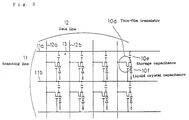
- Fig. 2 is a simple block diagram typically showing the structure of the pixel area of an active matrix circuit board
- Fig. 3 is a cross sectional diagram typically showing the basic structure of a liquid crystal display panel.
- active matrix circuit board 10 is divided into a pixel area 10a and drive circuit areas 10b, 10c (peripheral circuit part).
- Pixel region 13 is divided and formed in pixel area 10a by scanning lines (gate lines) 11a, 11b... (11) connected to drive circuit area 10b (scanning line drive circuit), and data lines 12a, 12b... (12) connected to drive circuit area 10c (data line drive circuit) as shown in Fig. 2.
- TFT 10d which switches between a state connecting and a state interrupting the data line 12 side and the pixel electrode side based on the scanning signal from scanning line 11, is formed in pixel region 13.
- a CMOS circuit is also formed in drive circuit areas 10b, 10c by thin-film transistors of a different conductive type.
- a small OFF current characteristic is required in TFT 10d of pixel area 10a so that a sufficient charge can be held in liquid crystal capacitance 10f.
- a thin-film transistor with a self-alignment structure is generally used in drive circuit areas 10b, 10c.
- liquid crystal capacitance 10f is the capacitance when active matrix circuit board 10 and counter circuit board 16 on which counter electrode 15 is formed are placed in opposition sandwiching liquid crystals 17 as shown in Fig. 3.
- three types of thin-film transistors including a pair of opposite conductive type thin-film transistors in the drive circuit area and a thin-film transistor in the pixel area, are formed because the characteristics required in the thin-film transistors are different in a built-in drive circuit type active matrix circuit board 10.
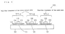
- Fig. 4 is a cross sectional diagram typically showing, of the thin-film transistors (hereafter "TFT") formed in the active matrix circuit board of the present embodiment, the structure of the TFT formed in the pixel area and the n-channel type TFT and p-channel type TFT formed in the drive circuit area.
- TFT thin-film transistors
- n-channel type TFT-A of the drive circuit area, p-channel type TFT-B of the drive circuit area, and n-channel type TFT-C of the pixel area are formed on a transparent insulated substrate 101 in order from the left side as looking at the figure.
- the CMOS circuit is formed in the drive circuit area by TFT-A and TFT-B.
- Gate insulation film 114 is formed on the surface side of channel formation area 111 and source-drain areas 112, 113, and gate electrode 115 is formed on the surface side of this gate insulation film 114 in TFT-A.
- Source-drain areas 112, 113 are n+ high concentration areas with an impurity concentration equal to or greater than 1 x 10¹⁹/cm3, e.g., 1 x 10²⁰/cm3, and are formed self-aligned to gate electrode 115.
- Gate insulation film 124 is formed on the surface side of channel formation area 121 and source-drain areas 122, 123, and gate electrode 125 is formed on the surface side of this gate insulation film 124 in TFT-B.
- Source-drain areas 122, 123 are p+ high concentration areas with an impurity concentration equal to or greater than 1 x 10¹⁹/cm3, e.g., 1 x 10²⁰/cm3, and are formed self-aligned to gate electrode 125.
- Gate insulation film 134 is formed on the surface side of channel formation area 131 and source-drain areas 132, 133, and gate electrode 135 is formed on the surface side of this gate insulation film 134 in TFT-C.
- Source-drain areas 132, 133 are formed as n ⁇ low density areas with an impurity concentration equal to or less than 1 x 10¹⁹/cm3, e.g., 5 x 10¹⁸/cm3, and are formed self-aligned to gate electrode 135.
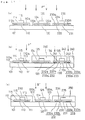
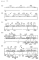
- Fig. 5 shows a process flow of the manufacturing method of the active matrix circuit board of the present embodiment.
- Silicon film 110 is a first silicon film for forming TFT-A in the drive circuit area
- silicon film 120 is a second silicon film for forming TFT-B in the drive circuit area
- Silicon film 130 is a third silicon film for forming TFT-C in the pixel area (first process).
- gate insulation films 114, 124, 134 are formed on the surface side of each silicon film 110, 120, 130 (second process).
- gate insulation films 114, 124, 134 the entire surface of insulated substrate 101
- a high concentration impurity is introduced into it.
- the polycrystalline silicon film into which an impurity was introduced is then patterned using photoetching technologies to form gate electrodes 115, 125, 135.
- the gate lines are simultaneously formed with the same materials when forming gate electrodes 115, 125, 135 (third process).
- the etching end point can be positively confirmed due to dry etching using CF4 plasma being used in the present embodiment for patterning the polycrystalline silicon film, the dimensions of the silicon film after patterning can be precisely controlled.
- low concentration phosphorus ions are implanted at a 5 x 10¹³/cm2 dose to silicon films 110, 120, 130 using gate electrodes 115, 125, 135 as a mask (low concentration area formation process).
- low concentration areas 110a, 120a, 130a with a 5 x 10¹⁸/cm3 impurity concentration are formed self-aligned to gate electrodes 115, 125, 135 in silicon films 110, 120, 130.
- Low concentration area 130a becomes source-drain areas 132, 133 of TFT-C without further ion implanting in the following processes.
- that part of silicon film 130 positioned directly below gate electrode 135 becomes channel formation area 131.
- low concentration area 110a becomes source-drain area 112, 133 (n+ high density area) with a 1 x 10²⁰/cm3 impurity concentration formed self-aligned to gate electrode 115.
- that part of silicon film 110 positioned directly below gate electrode 115 becomes channel formation area 111.
- low concentration area 120a becomes source-drain areas 122, 123 (p+ high density area) with a 1 x 10²⁰/cm3 impurity concentration formed self-aligned to gate electrode 125.
- that part of silicon film 120 positioned directly below gate electrode 125 becomes channel formation area 121.
- a low concentration impurity is also implanted to the drive circuit area side in the process forming the low concentration area on the pixel area side, and a high concentration area is formed there by the high concentration impurity implanted to the drive circuit area side. Therefore, the impurity concentration of each area can be separately controlled while holding the number of masking operations to a minimum. Therefore, a TFT having an optimal structure can be manufactured by the manufacturing method of the present embodiment without side etching the gate electrode. As a result, the display definition of the liquid crystal display panel can be improved because the ON current characteristic of the drive circuit area TFT and the OFF current characteristic of the pixel area TFT can be improved, and the electrical characteristics are stable.
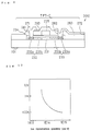
- Fig. 6 is a graph showing the relationship between the gate voltage Vg and drain current Id when the impurity concentration of the source-drain area is varied in an n-channel type TFT.
- solid line 5E13 shows the characteristics of the TFT with phosphorus implanted at a 5 x 10¹³/cm2 dose to the source-drain area.
- Solid line 1E14 shows the characteristics of the TFT with phosphorus implanted at a 1 x 10¹⁴/cm2 dose to the source-drain area.
- Solid line 5E14 shows the characteristics of the TFT with phosphorus implanted at a 5 x 10¹⁵/cm2 dose to the source-drain area.
- the ON current drops because the electrical resistance of the source-drain area increases as the dose is reduced. Furthermore, the OFF current drops because electrical field strength between the drain area and gate electrode is decreased in addition to the electrical resistance of the source-drain area increasing as the dose is reduced. Therefore, it is sufficient to form the source-drain area as a low concentration area in the pixel area TFT where a small OFF current is required.
- the impurity dose to the source-drain areas 132, 133 is less than or equal to 1 x 10¹⁴/cm2, and preferably less than 5 x 10¹³/cm2.
- the level of the TFT-C OFF current differs according to the setting conditions and the specifications of the liquid crystal display panel in which active matrix circuit board 100 is mounted, the impurity concentration of source-drain areas 132, 133 is set to an optimal level according to the specifications and setting conditions.
- the ON current of TFT-A and TFT-B in the drive circuit area is generally, however, preferably greater, and when gate voltage Vg is 10 V, drain current Id must be 10 ⁇ A or greater. Therefore, the impurity dose to the source-drain area of TFT-A and TFT-B must be approximately 1 x 10¹⁴/cm2 or greater.
- the TFT ON current and OFF current are also dependent on the film thickness of the polycrystalline silicon film in the channel formation area and the film thickness of the gate insulation film, in addition to the impurity concentration of the source-drain area.
- the electrical resistance of the source-drain area affecting the ON current and OFF current is also dependent on the film thickness and polycrystallinity of the source-drain area.
- the impurity concentration of the source-drain area is also affected by the ion energy during implantation and the film thickness of the gate insulation film. Therefore, the dosage is set as may be required with consideration for the ion energy and the film thickness of the gate insulation film.
- the structure of an active matrix circuit board according to the present embodiment is basically the same as the structure of the active matrix circuit board according to the first embodiment, and only that a pad area, which is a high concentration area, is formed in the source-drain area differs. Therefore, parts with functionality common to the first embodiment are identically labeled, and further identification in the figures and detailed description are omitted.
- Fig. 7 is a cross sectional diagram typically showing the structure of the pixel area TFT formed in an active matrix circuit board according to the present embodiment.
- source-drain areas 112, 113 of TFT-A are n+ high concentration areas with an impurity concentration of 1 x 10¹⁹/cm3 or greater, e.g., 1 x 10²⁰/cm3, and are formed self-aligned to gate electrode 115.
- Source-drain areas 112, 113 are composed of thin upper layer source-drain areas 112a, 113a and thick bottom layer source-drain areas 112b, 113b formed from a polycrystalline silicon film the same as channel formation area 111.
- Source-drain areas 122, 123 of TFT-B are p+ high concentration areas with an impurity concentration of 1 x 10¹⁹/cm3 or greater, e.g., 1 x 10²⁰/cm3, and are formed self-aligned to gate electrode 125.
- Source-drain areas 122, 123 are composed of thin upper layer source-drain areas 122a, 123a and thick bottom layer source-drain areas 122b, 123b formed from a polycrystalline silicon film the same as channel formation area 121.
- Source-drain areas 132, 133 of TFT-C are formed self-aligned to gate electrode 115, and are composed of thin upper layer source-drain areas 132a, 133a and thick bottom layer source-drain areas 132b, 133b formed from a polycrystalline silicon film the same as channel formation area 131.
- the top layer source-drain areas 132a, 133a are n ⁇ low concentration areas with an impurity concentration of 1 x 10¹⁹/cm3 or less, e.g., 5 x 10¹⁸/cm3.
- the bottom layer source-drain areas 132b, 133b are n+ high concentration areas with an impurity concentration of 1 x 10¹⁹/cm3 or greater, e.g., 1 x 10²⁰/cm3.
- source-drain areas 112, 113, 122, 123 are formed self-aligned to gate electrodes 115, 125, and, moreover, are formed as high concentration areas with a low electrical resistance. Furthermore, because source-drain areas 112, 113, 122, 123 are formed in two layers with a thick film thickness, the electrical resistance is low. Therefore, a high ON current can be obtained in TFT-A and TFT-B of the drive circuit area.
- source-drain areas 132b, 133b which are high concentration areas, are formed in source-drain areas 132, 133 of the TFT-C of the pixel area, the electrical resistance there is low and the ON current is thus high.
- that part of source-drain areas 132, 133 near the edge of gate electrode 135 in the TFT-C of the pixel area is the thin film thickness, low concentration area source-drain areas 132a, 133a, and a sufficiently low OFF current can therefore be obtained.
- high speed operation is possible in the drive circuit area and the written charge can be sufficiently maintained in the pixel area.
- active matrix circuit board 100a thus constructed, after forming a thick film thickness polycrystalline silicon film on the surface side of insulated substrate 101, this is patterned to form silicon films 161, 162, 163 for forming source-drain areas 112b, 113b, 122b, 123b, 132b, 133b of the bottom layer as shown in Fig. 8 (a).
- high concentration boron ions are implanted to silicon film 162 at a 1 x 10¹⁵/cm2 dose with silicon films 161, 163 masked by resist 164 to form source-drain areas 122b, 123b of the bottom layer.
- high concentration phosphorus ions are implanted to silicon films 161, 163 at a 1 x 10¹⁵/cm2 dose with silicon film 162 masked by resist 165 to form source-drain areas 112b, 113b, 132b, 133b of the bottom layer.
- Heat treatment is then applied to activate the implanted impurity. This activation may be applied after forming the other component areas during the heat treatment applied to activate those areas.
- an active matrix circuit board according to the present embodiment and the fourth and fifth embodiments described after this embodiment are basically the same as the structure of the active matrix circuit board according to the first embodiment, and only the structure of the TFT in the pixel area differs. Therefore, parts with functionality common to the first embodiment are identically labelled, and further identification in the figures and detailed description are omitted.
- Fig. 9 is a cross sectional diagram typically showing the structure of the TFT of the pixel area formed in an active matrix circuit board according to the present embodiment.
- the n-channel type TFT-C of the pixel area is formed over transparent insulated substrate 101 in Fig. 9, and n-channel type TFT-A and p-channel type TFT-B of the drive circuit area are formed over the same insulated substrate 101 as shown in Fig. 4.
- source-drain areas 112, 113, 122, 123 of TFT-A and TFT-B are high concentration areas with an impurity concentration of 1 x 10¹⁹/cm3 or greater, and are formed self-aligned to gate electrodes 115, 125.
- gate insulation film 234 is formed on the surface side of source-drain areas 232, 233 and channel formation area 231 in TFT-C, and gate electrode 235 is formed on the surface side of this gate insulation film 234.
- Layer insulation film 260 is formed on the surface side of gate electrode 235, source electrode 271 is connected to source-drain area 232 through the first contact hole 261, and pixel electrode 272 is connected to source-drain area 233 through second contact hole 262.
- those parts of source-drain areas 232, 233 corresponding to the openings of first contact hole 261 and second contact hole 262 are high concentration contact areas 232a, 233a with an impurity concentration of 1 x 10¹⁹/cm3 or greater, e.g., 1 x 10²⁰/cm3, and the remaining areas are low concentration source-drain areas 232b, 233b with an impurity concentration of 1 x 10¹⁹/cm3 or less, e.g., 5 x 10¹⁸/cm3. Therefore, that part of TFT-C positioned near the edge of gate electrode 235 is an LDD structure, i.e., low concentration source-drain areas 232b, 233b. As a result, the OFF current of TFT-C is small as shown by solid line 5E13 in Fig. 6.
- the TFT-C ON current is also high because high concentration contact areas 232a, 233a are formed in source-drain areas 232, 233. Specifically, in addition to the overall electrical resistance of the source-drain areas 232, 233 dropping due to high concentration contact areas 232a, 233a, the TFT-C ON current is high, equivalent to the characteristic shown by solid line 5E14 in Fig. 6 because the contact resistance of source-drain area 233 (drain area) and pixel electrode 272 formed from ITO is low.
- Fig. 10 is a graph showing the relationship between the dosage of impurity ions to the area connected by pixel electrode 272 formed from ITO and the contact resistance there. As shown in Fig. 10, if the dosage to source-drain area 233 is increased, the contact resistance tends to drop, and the contact resistance becomes severely low in particular when the dosage exceeds 1 x 10¹⁴/cm2.
- source electrode 271 which is an aluminum electrode
- source-drain area 232 source area
- the contact resistance tends to drop the higher the impurity concentration in the area to which source electrode 271 connects.
- the contact resistance of aluminum and polycrystalline silicon is basically low, the contribution to improving the ON current characteristic is less than when the contact resistance of the pixel electrode 272 and source-drain area 233 is reduced.
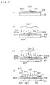
- Fig. 11 shows a process flow of the manufacturing method of the active matrix circuit board of this embodiment.
- Silicon film 110 is a first silicon film for forming TFT-A
- silicon film 120 is a second silicon film for forming TFT-B
- Silicon film 230 is a third silicon film for forming TFT-C (first process).
- gate insulation films 114, 124, 234 are formed on the surface side of each silicon film 110, 120, 230 (second process).
- gate insulation films 114, 124, 134 the entire surface of insulated substrate 201
- a high concentration impurity is introduced into it.
- the polycrystalline silicon film is then patterned using photoetching technologies to form gate electrodes 115, 125, 235.
- the gate lines are simultaneously formed with the same materials when forming gate electrodes 115, 125, 235 (third process).
- phosphorus ions are implanted at a 5 x 10¹³/cm2 dose to silicon films 110, 120, 230 using gate electrodes 115, 125, 235 as a mask.
- low concentration areas 110a, 120a, 230a with a 5 x 10¹⁸/cm3 impurity concentration are formed self-aligned to gate electrodes 115, 125, 235 in silicon films 110, 120, 230 (low concentration area formation process).
- Openings 241, 242 are formed here in that part of low concentration area 230a of silicon film 230 corresponding to where the high concentration contact areas 232a, 233a are to be formed.
- high concentration phosphorus ions are implanted at a 1 x 10¹⁵/cm2 dose to silicon films 110, 230 as shown by arrow P+ (fourth process).
- low concentration area 110a becomes source-drain areas 112, 133 (n+ high concentration area) with a 1 x 10²⁰/cm3 impurity concentration formed self-aligned to gate electrode 115.
- high concentration contact areas 232a, 233a with an impurity concentration of 1 x 10²⁰/cm3 are formed in low concentration area 230a of silicon film 230, and that part to which high concentration ions were not implanted becomes low concentration source-drain areas 232b, 233b with an impurity concentration of 5 x 10¹⁸/cm3.
- that part of silicon film 230 positioned directly below gate electrode 235 becomes channel formation area 231.
- low concentration area 120b becomes source-drain areas 122, 123 (p+ high concentration areas) with a 1 x 10²⁰/cm3 impurity concentration formed self-aligned to gate electrode 125.
- the dosage conditions can be independently set for the n-channel type TFT-A of the drive circuit area, the p-channel type TFT-B of the drive circuit area, and the n-channel type TFT-C of the pixel area by means of the manufacturing method of this embodiment as thus described, a TFT with optimum electrical characteristics can be manufactured. Furthermore, because high concentration contact areas 232a, 233a are formed while forming the LDD structure by twice implanting ions to source-drain areas 232, 233 in TFT-C, the electrical resistance and the contact resistance of the overall source-drain areas 232, 233 can be reduced with the OFF current held low.
- the low concentration area formation process can be applied after either the third, fourth, or fifth process.
- the order of the fourth and fifth processes can be reversed.
- Fig. 12 is a cross sectional diagram typically showing the structure of the TFT of the pixel area formed in an active matrix circuit board according to the present embodiment.
- the n-channel type TFT-C of the pixel area is formed over transparent insulated substrate 101 in Fig. 12, and n-channel type TFT-A and p-channel type TFT-B of the drive circuit area are formed over the same insulated substrate 101 as shown in Fig. 4.
- source-drain areas 112, 113, 122, 123 of TFT-A and TFT-B are high concentration areas with an impurity concentration of 1 x 10¹⁹/cm3 or greater, e.g., 1 x 10²⁰/cm3, and are formed self-aligned to gate electrodes 115, 125.
- gate insulation film 334 is formed on the surface side of source-drain areas 332, 333 and channel formation area 331 in TFT-C, and gate electrode 335 is formed on the surface side of this gate insulation film 334.
- Layer insulation film 360 is formed on the surface side of gate electrode 335, source electrode 371 is connected to source-drain area 332 through the first contact hole 361, and pixel electrode 372 is connected to source-drain area 333 through second contact hole 362.
- TFT-C has an offset gate structure formed at a position approximately 2 ⁇ m removed in the lateral direction from the edge of gate electrode 335 with the source-drain areas 332, 333 as high concentration areas with an impurity concentration of 1 x 10¹⁹/cm3 or greater, e.g., 1 x 10²⁰/cm3.
- TFT-C therefore has a small OFF current.
- the distance in the lateral direction between gate electrode 335 and the source-drain area in TFT-C is set to approximately 2 ⁇ m, the drop in the ON current resulting from the offset structure is held to a minimum.
- the contact resistance of the drain electrode formed from ITO and the source-drain areas 332, 333 is low.
- TFT-A and TFT-B have a high ON current because of their self-aligned structure.
- Fig. 13 is a process cross section showing the manufacturing method of the active matrix circuit board of this embodiment.
- the ion implantation performed in the process shown in Fig. 11 (a) in the manufacturing method associated with the third embodiment is not performed.
- the polycrystalline silicon film formed over insulated substrate 101 is patterned form silicon films 110, 120, 330.
- Silicon film 110 is a first silicon film for forming TFT-A
- silicon film 120 is a second silicon film for forming TFT-B.
- Silicon film 330 is a third silicon film for forming TFT-C (first process).
- gate insulation films 114, 124, 334 are formed on the surface side of each silicon film 110, 120, 330 (second process).
- gate insulation films 114, 124, 334 the entire surface of insulated substrate 201
- a high concentration impurity is introduced into it.
- the polycrystalline silicon film is then patterned using photoetching technologies to form gate electrodes 115, 125, 335. (third process).
- Openings 341, 342 are formed here in that part of resist 340 corresponding to where source-drain areas 332, 333 are to be formed in silicon film 330.
- high concentration phosphorus ions are implanted at a 1 x 10¹⁵/cm2 dose to silicon films 110, 330 as shown by arrow P+ (fourth process).
- source-drain areas 112, 133 (n+ high concentration area) with a 1 x 10²⁰/cm3 impurity concentration are formed self-aligned to gate electrode 115 in silicon film 110.
- offset gate structure source-drain areas 332, 333 are formed in silicon film 330 with an impurity concentration of 1 x 10¹⁹/cm3 or greater. That part of silicon film 330 to which ions were not implanted becomes channel formation area 331.
- silicon film 120 becomes source-drain areas 122, 123 (p+ high concentration areas) with a 1 x 10²⁰/cm3 impurity concentration formed self-aligned to gate electrode 125.
- the dosage conditions can be independently set for TFT-A, TFT-B, and TFT-C by means of the manufacturing method of this embodiment as thus described, formation under optimal conditions is possible. Furthermore, over-etching for gate electrode 335 is not necessary when forming TFT-C with an offset gate structure. As a result, the gate length of TFT-C is stable, and a high reliability active matrix circuit board 300 can be manufactured.
- the structure of the active matrix circuit board of this embodiment is basically the same as the structure of the active matrix circuit board of the fourth embodiment, and is characterized by forming a pad area, which is a high concentration area, only in the source-drain area of the n-channel type TFT.
- Fig. 14 is a cross sectional diagram typically showing the structure of the TFT formed in an active matrix circuit board according to the present embodiment.
- gate insulation film 414 is formed on the surface side of channel formation area 411 and source-drain areas 412, 413 in TFT-A, and gate electrode 415 is formed on the surface side of this gate insulation film 414.
- Source-drain areas 412, 413 are n+ high concentration areas with an impurity concentration of 1 x 10¹⁹/cm3, e.g., 1 x 10²⁰/cm3, formed self-aligned to gate electrode 415.
- Source-drain areas 412, 413 comprise thin top layer source-drain areas 412a, 413a formed from the same polycrystalline silicon film as channel formation area 411, and thick bottom layer source-drain areas 412b, 413b.
- Gate insulation film 124 is formed on the surface side of channel formation area 121 and source-drain areas 122, 123, and gate electrode 125 is formed on the surface side of this gate insulation film 124 in TFT-B.
- Source-drain areas 122, 123 are p+ high density areas with an impurity concentration equal to or greater than 1 x 10¹⁹/cm3, e.g., 1 x 10²⁰/cm3, and are formed self-aligned to gate electrode 125.
- Gate insulation film 434 is formed on the surface side of channel formation area 431 and source-drain areas 432, 433, and gate electrode 435 is formed on the surface side of this gate insulation film 434 in TFT-C.
- Source-drain areas 432, 433 comprise thin top layer source-drain areas 432a, 433a formed from the same polycrystalline silicon film as channel formation area 431, and thick bottom layer source-drain areas 432b, 433b.
- Top layer source-drain areas 432a, 433a are non-doped areas.
- Bottom layer source-drain areas 432b, 433b are n+ high concentration areas with an impurity concentration of 1 x 10¹⁹/cm3, e.g., 1 x 10²⁰/cm3.
- that part of top layer source-drain areas 432a, 433a positioned near the edge of gate electrode 435 becomes non-doped offset areas 432c, 433c.
- the source electrodes and drain electrodes of TFT-A and TFT-C are connected to bottom layer source-drain areas 412b, 413b, 432b, 433b.
- source-drain areas 412, 413, 122, 123 are formed self-aligned to gate electrodes 415, 125, and are formed as high concentration areas with a low electrical resistance. Furthermore, because source-drain areas 412, 413 are formed in two layers with a thick film thickness, the electrical resistance is low. Therefore, a high ON current can be obtained in TFT-A and TFT-B of the drive circuit area.
- the silicon film is patterned to form silicon films 401, 402, 403 as shown in Fig. 15 (a).
- Silicon film 410 is the first silicon film for forming TFT-A
- silicon film 120 is a second silicon film for forming TFT-B
- Silicon film 420 is the third silicon film for forming TFT-C (first process).
- gate insulation films 414, 124, 434 are formed on the surface side of each silicon film 410, 120, 430 (second process), and then gate electrodes 415, 125, 435 are formed (third process).
- source-drain areas 412, 433 with a 1 x 10²⁰/cm3 impurity concentration formed self-aligned to gate electrode 415.
- a resist mask with openings formed in that part of silicon film 430 corresponding to where source-drain areas 432b, 433b of the bottom layer are to be formed can be used here.
- all of source-drain areas 432, 433 except for the offset area can be formed as n+ high concentration areas.
- source-drain areas 122, 123 which are p+ high concentration areas, are formed self-aligned to gate electrode 125 in silicon film 120.
- the manufacturing method of a conductive silicon film is described as the sixth embodiment.
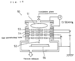
- Fig. 16 is a structural diagram of the ion implantation device used to manufacture the n-type conductive silicon film of this embodiment.
- an extraction electrode 53 for extracting impurity ions 52 from plasma source 51, and acceleration electrode 54 for accelerating the impurity ions 52 to a predetermined energy level are provided in ion implantation machine 50, and a voltage is applied to extraction electrode 53 and acceleration electrode 54.
- impurity ions 52 extracted from plasma source 51 can be implanted to the polycrystalline silicon film formed on the surface of glass substrate 55.
- a mass separator for applying mass separation to the ions generated from the dopant gas is not provided in ion implantation machine 50, and all ions generated from the dopant gas are implanted to the polycrystalline silicon film without mass separation.
- a polycrystalline silicon film with a thickness of, for example, 500 ⁇ is first formed on the surface of a glass substrate, and on the surface of the polycrystalline silicon film is formed a 1200 ⁇ thick silicon dioxide film (SiO2 film).
- SiO2 film silicon dioxide film
- the dosage of the ions implanted at this time is 1 x 10¹⁴/cm2 converted to P+ ions.
- the P+ ion concentration peak in the polycrystalline silicon film will be approximately 1 x 10¹⁹/cm3.
- ions generated from a 100% pure hydrogen gas are implanted to the polycrystalline silicon film through the silicon dioxide film at a 20 keV energy level without mass separation (second ion doping process).
- most of the ions generated from the pure hydrogen gas are H2+, and by setting the implantation energy level to 20 keV in this case, the concentration peak in the H2+ depth direction can be controlled to be positioned at the boundary of the polycrystalline silicon film and the silicon dioxide film.
- Heat treatment with a temperature of approximately 300°C is then applied for approximately one hour to the polycrystalline silicon film implanted with an impurity (P+ ions) (heating process).
- the heat treatment temperature here is in the range from approximately 300°C to approximately 600°C, and preferably in the range from approximately 300°C to approximately 550°C. Furthermore, in the TFT manufacturing process, when a low-cost glass substrate is used as the insulated substrate, the heat treatment temperature is preferably set within the range from approximately 300°C to approximately 450°C.
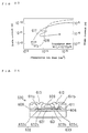
- Fig. 17 The relationship between the hydrogen ion dose to the polycrystalline silicon film thus formed and the sheet resistance is shown in Fig. 17.
- Fig. 17 the hydrogen ion does is converted to a H+ ion quantity.
- the resistance of the polycrystalline silicon implanted with a small quantity of impurity is low when the dose of implanted H+ ions is in the range from 1 x 10¹⁴/cm2 to 1 x 10¹⁵/cm2, or specifically when the concentration peak of H+ ions in the polycrystalline silicon film is in the range from 6 x 10¹⁸/cm3 to 1 x 10²⁰/cm3.
- the reasons for this are believed to be the result of competition between the effect of dangling bonds in the polycrystalline silicon film terminating due to hydrogen ion implantation, and the effect of defects being created by hydrogen ion implantation.
- Fig. 18 the relationship between the phosphorus ion dose in the first doping process and sheet resistance is shown in Fig. 18 when the conditions of the second ion doping process are set so that ions generated from pure hydrogen are implanted without mass separation to the polycrystalline silicon film at a dose from 1 x 10¹⁴/cm2 to 1 x 10¹⁵/cm2 to achieve a concentration peak of H+ ions in the polycrystalline silicon film in the range from 6 x 10¹⁸/cm3 [sic] to 1 x 10²⁰/cm3.
- the phosphorus ions are shown converted to a P+ ion quantity.
- the sheet resistance drops if the P+ ion dose is changed to the range from 5 x 10¹²/cm2 to 1.5 x 10¹⁵/cm2, and the P+ ion concentration peak is increased from 5 x 10¹⁷/cm3 to 1.6 x 10¹⁹/cm3.
- a low concentration polycrystalline silicon film can be made conductive according to this embodiment by heat treatment at a relatively low temperature of approximately 300°C by implanting ions generated from a pure hydrogen gas to the silicon film without mass separation after implanting all ions generated from a mixed gas, which contains an impurity gas for generating an impurity with the remainder being hydrogen, to the silicon film without mass separation.
- a mixed gas which contains an impurity gas for generating an impurity with the remainder being hydrogen
- the energy level during ion implantation is a property that must be set to the optimum conditions based on the thickness and type of the silicon dioxide film formed on the surface of the polycrystalline silicon film, and the type of ions implanted, and there is therefore no limit on the conditions.
- the concentration peak in the H+ depth direction can be controlled to a position at the boundary of the polycrystalline silicon film and the silicon dioxide film.
- the thickness of the silicon dioxide film is approximately 800 ⁇
- all ions generated from a mixed gas containing 5% PH3 with the remainder being hydrogen are implanted to the polycrystalline silicon film through the silicon dioxide film at a 50 keV energy level without mass separation.
- the ion dose is set to 6.5 x 10¹³/cm2 converted to P+ ions (first doping process).
- ions generated from pure hydrogen are implanted to the polycrystalline silicon film through the silicon dioxide film at a 12 keV energy level without mass separation (first doping process).
- the manufacturing method of a p-type conductive silicon film is described as the seventh embodiment. It is to be noted that the ion implantation machine 50 used in the sixth embodiment is also used in this embodiment, and with this device all ions generated from the dopant gas are implanted to the polycrystalline silicon film without mass separation.
- a polycrystalline silicon film with a thickness of, for example, 500 ⁇ is first formed on the surface of a glass substrate, and on the surface of the polycrystalline silicon film is formed a 1200 ⁇ thick silicon dioxide film (SiO2 film).
- SiO2 film silicon dioxide film
- the dosage of the ions implanted at this time is 1 x 10¹⁴/cm2 converted to B+ ions.
- the B+ ion concentration peak in the polycrystalline silicon film will be approximately 1 x 10¹⁹/cm3.
- ions generated from a 100% pure hydrogen gas are implanted to the polycrystalline silicon film through the silicon dioxide film at a 20 keV energy level without mass separation (second ion doping process).
- most of the ions generated from the pure hydrogen gas are H2+, and by setting the implantation energy level to 20 keV in this case, the concentration peak in the H2+ depth direction can be controlled to be positioned at the boundary of the polycrystalline silicon film and the silicon dioxide film.
- Heat treatment with a temperature of approximately 300°C is then applied for approximately one hour to the polycrystalline silicon film implanted with an impurity (B+ ions) (heating process).
- the heat treatment temperature here is in the range from approximately 300°C to approximately 600°C, and preferably in the range from approximately 300°C to approximately 550°C. Furthermore, in the TFT manufacturing process, when a low-cost glass substrate is used as the insulated substrate, the heat treatment temperature is preferably set within the range from approximately 300°C to approximately 450°C.
- the resistance of the polycrystalline silicon implanted with a small quantity of impurity is low when the dose of implanted H+ ions is in the range from 1 x 10¹⁴/cm2 to 1 x 10¹⁵/cm2, or specifically when the concentration peak of H+ ions in the polycrystalline silicon film is in the range from 6 x 10¹⁸/cm3 to 1 x 10²⁰/cm3.
- the reasons for this are believed to be the result of competition between the effect of irregular bonds in the polycrystalline silicon film terminating due to hydrogen ion implantation, and the effect of defects being created by hydrogen ion implantation.
- Fig. 20 the relationship between the boron ion dose in the first doping process and sheet resistance is shown in Fig. 20 when the conditions of the second ion doping process are set so that ions generated from pure hydrogen are implanted without mass separation to the polycrystalline silicon film at a dose from 1 x 10¹⁴/cm2 to 1 x 10¹⁵/cm2 to achieve a concentration peak of H+ ions in the polycrystalline silicon film in the range from 6 x 10¹⁸/cm3 [sic] to 1 x 10²⁰/cm3.
- the boron ion is shown converted to a B+ ion quantity.
- the sheet resistance drops if the B+ ion dose is changed to the range from 5 x 10¹²/cm2 to 1.5 x 10¹⁵/cm2, and the B+ ion concentration peak is increased from 5 x 10¹⁷/cm3 to 1.6 x 10¹⁹/cm3.
- a low concentration polycrystalline silicon film can be made conductive according to this embodiment by heat treatment at a relatively low temperature of approximately 300°C by implanting ions generated from a pure hydrogen gas to the silicon film without mass separation after implanting all ions generated from a mixed gas, which contains an impurity gas for generating an impurity with the remainder being hydrogen, to the silicon film without mass separation.
- the energy level during ion implantation is a property that must be set to the optimum conditions based on the thickness and type of the silicon dioxide film formed on the surface of the polycrystalline silicon film, and the type of ions implanted, and there is therefore no limit on the conditions.
- the concentration peak in the H+ depth direction can be positioned at the boundary of the polycrystalline silicon film and the silicon dioxide film.
- implantation can use an energy level of approximately 40 keV when primarily B+ ions are generated even though ions were implanted at 80 keV in this embodiment.
- a method for manufacturing TFT applying the manufacturing method of a conductive silicon film associated with the sixth embodiment is described with reference to Fig. 21 and Fig. 22.
- Fig. 21 is a cross section typically showing the structure of a TFT formed on a glass substrate using the manufacturing method of this embodiment, and Fig. 22 shows a process flow of the manufacturing method.
- silicon dioxide film 606 for preventing diffusion of heavy metals from glass substrate 601 to the device area is formed on the surface of glass substrate 601, and on its surface are formed an approximately 500 ⁇ thick polycrystalline silicon film that will become channel formation area 607 and source-drain areas 602, 603 formed as n ⁇ -type low concentration areas.
- gate insulation film 608 On the surface of source-drain areas 602, 603 and channel formation area 607 is formed gate insulation film 608 from an approximately 1200 ⁇ thick silicon dioxide film (SiO2).
- gate electrode 609 from tantalum, aluminum, or chrome
- TFT 620 is formed from gate electrode 609, source-drain areas 602, 603, and channel formation area 607.
- Source-drain areas 602, 603 are low concentration areas formed self-aligned to gate electrode 609 with a concentration peak of phosphorus ions as the impurity from 3 x 10¹⁸/cm3 to 1 x 10¹⁹/cm3.
- Layer insulation film 611 is formed on the surface side of gate electrode 609, and aluminum source electrode 613 is connected to source-drain area 602 (source area), and aluminum and ITO drain electrode 612 is connected to source-drain area 603 (drain area), through contact holes 611a, 611b.
- silicon dioxide film 606 is formed as an insulation film with a film thickness of approximately 2000 ⁇ on the surface of glass substrate 601 as shown in Fig. 22 (a). This silicon dioxide film 606 is formed for the purpose of preventing diffusion of heavy metals, etc., contained in glass substrate 601 to the element side, and can therefore be omitted when using a substrate of sufficient purity.
- the crystallization rate of polycrystalline silicon film 604 is preferably approximately 75% or higher, and is even more preferably 90% or higher (first process).
- gate insulation film 608 is formed from SiO2 with a film thickness of approximately 1200 ⁇ on the surface of polycrystalline silicon film 604 (second process).
- gate insulation film 608 a low electrical resistance metal layer such as aluminum, chrome or tantalum is formed by sputtering, etc., to a film thickness of approximately 6000 ⁇ , and this is then patterned to form gate electrode 609 (third process).
- a low electrical resistance metal layer such as aluminum, chrome or tantalum is formed by sputtering, etc., to a film thickness of approximately 6000 ⁇ , and this is then patterned to form gate electrode 609 (third process).
- polycrystalline silicon film 604 becomes low concentration area 604a with a phosphorus ion concentration peak in the range from 3 x 10¹⁸/cm3 to 1 x 10¹⁹/cm3.
- the hydrogen ion concentration peak in low concentration area 604a is in the range from 6 x 10¹⁸/cm3 to 1 x 10²⁰/cm3.
- the impurity is activated in polycrystalline silicon film 604 (low concentration area 604a) implanted with the impurity by heat treatment for approximately one hour at approximately 300°C in a nitrogen atmosphere (heating process).
- contact holes 609a, 609b are formed after forming layer insulation film 611 on the surface of gate electrode 609, and source electrode 613 and drain electrode 612 are connected to source-drain areas 602, 603.
- the OFF current in TFT 620 can be reduced when the P+ dose is in the range from 3 x 10¹³/cm2 to 1 x 10¹⁴/cm2, in other words when the phosphorus ion concentration peak in the polycrystalline silicon film (source-drain areas 602, 603) is in the range from 3 x 10¹⁸/cm3 to 1 x 10¹⁹/cm3.
- a low cost glass substrate 601 can be used because a heat treatment temperature of approximately 300°C can be used with the TFT manufacturing method of the present embodiment.
- a low electrical resistance electrode material can be used without being restricted by heat resistance.
- mass separation is not used in any of the ion doping processes, ions can be implanted to a wide area of the substrate.
- Fig. 24 is a cross section typically showing the structure of a TFT formed on a glass substrate using the manufacturing method of this embodiment, and Fig. 25 shows a process flow of the manufacturing method. It is to be noted that the basic configuration of the eight embodiment is common to the TFT of this embodiment and the TFT of embodiments 10 through 13 described below, and only the configuration of the source-drain area differs. Therefore, the same symbols are applied to parts having common functionality, and detailed description thereof is omitted.
- an n-channel type TFT 630 comprising gate electrode 609 of tantalum, aluminum, or chrome, gate insulation film 608, source-drain areas 632, 633 formed self-aligned to gate electrode 609, and channel formation area 607 is formed on the surface of glass substrate 601.
- High concentration contact areas 632a, 633a positioned in the area corresponding to contact holes 611a, 611b, and low concentration source-drain areas 632b, 633b positioned on the side of the edge of gate electrode 609 are formed in source-drain areas 632, 633, and TFT 630 has an LDD structure.
- the phosphorus ion concentration peak of the low concentration source-drain areas 632b, 633b here is in the range from 3 x 10¹⁸/cm3 to 1 x 10¹⁹/cm3, and the phosphorus ion concentration peak in high concentration contact areas 632a, 633a is 1 x 10²⁰/cm3 or higher.
- the overall electrical resistance of source-drain areas 632, 633 is low due to the low electrical resistance high concentration contact areas 632a, 633a. Moreover, because it is low concentration source-drain areas 632b, 633b that are positioned near the edge of gate electrode 609, the OFF current is low. Furthermore, because source electrode 613 and drain electrode 612 are connected to source-drain areas 632, 633 through high concentration contact areas 632a, 633a, the contact resistance is low. In particular, even if drain electrode 612 is made of ITO as the pixel electrode, the contact resistance can be reduced because ITO is connected to high concentration contact area 633a.
- silicon dioxide film 606 is formed as an insulation film with a film thickness of approximately 2000 ⁇ on the surface of glass substrate 601.
- the crystallization rate of polycrystalline silicon film 604 is preferably approximately 75% or higher, and is even more preferably 90% or higher (first process).
- gate insulation film 608 is formed from SiO2 with a film thickness of approximately 1200 ⁇ on the surface of polycrystalline silicon film 604 (second process).
- gate insulation film 608 a low electrical resistance metal layer such as aluminum, chrome or tantalum is formed by sputtering, etc., to a film thickness of approximately 6000 ⁇ , and this is then patterned to form gate electrode 609 (second process).
- a low electrical resistance metal layer such as aluminum, chrome or tantalum is formed by sputtering, etc., to a film thickness of approximately 6000 ⁇ , and this is then patterned to form gate electrode 609 (second process).
- polycrystalline silicon film 604 becomes low concentration area 604a with a phosphorus ion concentration peak in the range from 3 x 10¹⁸/cm3 to 1 x 10¹⁹/cm3.
- the hydrogen ion concentration peak in low concentration area 604a is in the range from 6 x 10¹⁸/cm3 to 1 x 10²⁰/cm3.
- contact holes 611a, 611b are formed in layer insulation film 611 after forming layer insulation film 611 on the surface of gate electrode 609.
- a ions shown by arrow Ion-3 generated from a doping gas of 5% PH3 with the remainder H2 gas are implanted to low concentration area 604a to achieve a P+ ion dose of 1 x 10¹³/cm2 or greater, forming high concentration contact areas 623a, 633a with a phosphorus ion concentration peak of 1 x 10²⁰/cm3 in the area corresponding to the bottom of contact holes 611a, 611b.
- the impurity ions are implanted at an approximately 30 keV energy level so that the impurity concentration peak will be positioned at the center in the depth direction of polycrystalline silicon film 604 at the bottom side of contact holes 611a, 611b (fifth process).
- the impurity is activated by heat treatment of polycrystalline silicon film 604 implanted with the impurity for approximately one hour at approximately 300°C in a nitrogen atmosphere (heating process).
- source-drain areas 632, 633 that part of polycrystalline silicon film 604 to which the impurity was introduced becomes source-drain areas 632, 633. That part of source-drain areas 632, 633 implanted with a high concentration impurity is high concentration contact areas 632a, 633a, and the other area is low concentration source areas 632b, 633b.
- the area corresponding to directly below gate electrode 609 is channel formation area 607.
- source electrode 613 and drain electrode 612 are connected to high concentration contact areas 632a, 633a, respectively.
- Fig. 26 is a cross section typically showing the structure of a TFT formed on a glass substrate using the manufacturing method of this embodiment, and Fig. 27 shows a process flow of the manufacturing method.
- an n-channel type TFT 640 comprising gate electrode 609 of tantalum, aluminum, or chrome, gate insulation film 608, source-drain areas 632, 633 formed self-aligned to gate electrode 609, and channel formation area 607 is formed on the surface of glass substrate 601.
- High concentration contact areas 642a, 643a with a phosphorus ion concentration peak of 1 x 10²⁰/cm3 or greater is formed in the area of source-drain areas 642, 643 including the bottom surface of contact holes 611a, 611b, and positioned near the edge of gate electrode 609 are low concentration source-drain areas 642b, 643b with a phosphorus ion concentration peak in the range from 3 x 10¹⁸/cm3 to 1 x 10¹⁹/cm3.
- the overall electrical resistance of source-drain areas 642, 643 is low due to the low electrical resistance high concentration contact areas 642a, 643a.
- the contact resistance is low because source electrode 613 and drain electrode 612 are connected to source-drain areas 642, 643 through high concentration contact areas 642a, 643a.
- the contact resistance is low even if drain electrode 612 is made from ITO as the pixel electrode because ITO is connected to high concentration contact area 643a.
- silicon dioxide film 606 is formed as an insulation film with a film thickness of approximately 2000 ⁇ on the surface of glass substrate 601.
- the crystallization rate of polycrystalline silicon film 604 is preferably approximately 75% or higher, and is even more preferably 90% or higher (first process).
- gate insulation film 608 is formed from SiO2 with a film thickness of approximately 1200 ⁇ on the surface of polycrystalline silicon film 604 (second process).
- a low electrical resistance metal layer such as aluminum, chrome or tantalum is formed by sputtering, etc., to a film thickness of approximately 6000 ⁇ , and this is then patterned to form gate electrode 609 (third process).
- polycrystalline silicon film 604 becomes low concentration area 604a with a phosphorus ion concentration peak in the range from 3 x 10¹⁸/cm3 to 1 x 10¹⁹/cm3.
- the hydrogen ion concentration peak in low concentration area 604a is in the range from 6 x 10¹⁸/cm3 to 1 x 10²⁰/cm3.
- layer insulation film 611 made from a SiO2 film with a 5000 ⁇ film thickness is formed on the surface of gate electrode 609, and then contact holes 611a, 611b are formed in layer insulation film 611.
- the impurity is activated by heat treatment of polycrystalline silicon film 604 implanted with the impurity for approximately one hour at approximately 300°C in a nitrogen atmosphere (heating process).
- source-drain areas 642, 643 that part of polycrystalline silicon film 604 to which the impurity was introduced becomes source-drain areas 642, 643. That part of source-drain areas 642, 643 implanted with a high concentration impurity is high concentration contact areas 642a, 643a, and the other area is low concentration source areas 642b, 643b.
- the area corresponding to directly below gate electrode 609 is channel formation area 607.
- source electrode 613 and drain electrode 612 are connected, respectively, to high concentration contact areas 642a, 643a through contact holes 611a, 611b of layer insulation film 611.
- the implantation energy can be increased in the present embodiment when forming high concentration contact areas 642a, 643a because the impurity ions are implanted to the silicon film through gate insulation film 608.
- the productivity of TFT 640 manufacture can be improved in addition to the effects obtained with the eighth embodiment because of the advantage of being able to set the ion beam current high.
- Fig. 28 is a cross section typically showing the structure of a TFT formed on a glass substrate using the manufacturing method of this embodiment, and Fig. 29 [sic] shows a process flow of the manufacturing method.
- an n-channel type TFT 650 comprising gate electrode 609 of tantalum, aluminum, or chrome, gate insulation film 608, source-drain areas 652, 653 formed self-aligned to gate electrode 609, and channel formation area 607 is formed on the surface of glass substrate 601.
- Source-drain areas 652, 653 are low concentration areas with a phosphorus ion concentration peak in the range from 3 x 10¹⁸/cm3 to 1 x 10¹⁹/cm3, and have a double layer structure comprising low concentration source-drain areas 652a, 653a on the bottom with a film thickness of approximately 1000 ⁇ , and low concentration source-drain areas 652b, 653b on the top with a film thickness of approximately 500 ⁇ .
- the top layer low concentration source-drain areas 652b, 653b are areas formed from the same polycrystalline silicon film as channel formation area 607.
- source-drain areas 652, 653 have an overall low electrical resistance because the overall film thickness is thick. Moreover, because what is positioned near the edge of gate electrode 609 is the thin low concentration source-drain areas 652b, 653b of the top layer, the OFF current is low. This is believed to be because the number of trap levels decreases the thinner the film thickness.
- the manufacturing method of a TFT thus configured is described with reference to Fig. 29.
- silicon dioxide film 606 is formed as an insulation film with a film thickness of approximately 2000 ⁇ on the surface of glass substrate 601.
- the crystallization rate of polycrystalline silicon films 604 and 605 is preferably approximately 75% or higher, and is even more preferably 90% or higher (first process).
- gate insulation film 608 is formed from SiO2 with a film thickness of approximately 1200 ⁇ on the surface of polycrystalline silicon film 604 (second process).
- gate insulation film 608 a low electrical resistance metal layer such as aluminum, chrome or tantalum is formed by sputtering, etc., to a film thickness of approximately 6000 ⁇ , and this is then patterned to form gate electrode 609 (third process).
- a low electrical resistance metal layer such as aluminum, chrome or tantalum is formed by sputtering, etc., to a film thickness of approximately 6000 ⁇ , and this is then patterned to form gate electrode 609 (third process).
- low concentration areas 604a, 605a with a phosphorus ion concentration peak in the range from 3 x 10¹⁸/cm3 to 1 x 10¹⁹/cm3 are formed in polycrystalline silicon films 604 and 605.
- the hydrogen ion concentration peak in low concentration areas 604a, 605a is in the range from 6 x 10¹⁸/cm3 to 1 x 10²⁰/cm3.
- the impurity is activated by heat treatment of polycrystalline silicon film 604 implanted with the impurity for approximately one hour at approximately 300°C in a nitrogen atmosphere (heating process).
- layer insulation film 611 is formed from an SiO2 film with a film thickness of 5000 ⁇ on the surface of gate electrode 609, and contact holes 611a, 611b are then formed in layer insulation film 611.
- contact holes 611a, 611b in layer insulation film 611 can be sufficiently over-etched when formed by dry etching because the bottom side is a double layer structure with a bottom layer of low concentration source-drain areas 652a, 653a and a top layer of low concentration source-drain areas 652b, 653b.
- the stability of the manufacturing process is improved in addition to the effects obtained by the eighth embodiment.
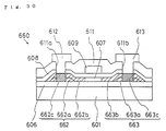
- Fig. 30 is a cross section typically showing the structure of a TFT formed on a glass substrate using the manufacturing method of this embodiment, and Fig. 31 shows a process flow of the manufacturing method.
- an n-channel type TFT 660 comprising gate electrode 609 of tantalum, aluminum, or chrome, gate insulation film 608, source-drain areas 662, 663 formed self-aligned to gate electrode 609, and channel formation area 607 is formed on the surface of glass substrate 601.
- Source-drain areas 662, 663 have a double layer structure comprising low concentration source-drain areas 662a, 663a on the bottom with a film thickness of approximately 1000 ⁇ , and low concentration source-drain areas 662b, 663b on the top with a film thickness of approximately 500 ⁇ .
- These low concentration source-drain areas 662a, 662b, 663a, 663b are low concentration areas with a phosphorus ion concentration peak in the range from 3 x 10¹⁸/cm3 to 1 x 10¹⁹/cm3.
- the top layer low concentration source-drain areas 662b, 663b are areas formed from the same polycrystalline silicon film as channel formation area 607.
- high concentration contact areas 662c, 663c with a phosphorus ion concentration peak of 1 x 10²⁰/cm3 or higher are formed at the position corresponding to the opening of contact holes 611a, 611b from the surface side of the top layer low concentration source-drain areas 662b, 663b to the bottom side of the bottom layer low concentration source-drain areas 662a, 663a.
- source-drain areas 662, 663 have an overall low electrical resistance because the overall film thickness is thick. Moreover, because what is positioned near the edge of gate electrode 609 is the thin low concentration source-drain areas 662b, 663b of the top layer, the OFF current is low.
- silicon dioxide film 606 is formed as an insulation film with a film thickness of approximately 2000 ⁇ on the surface of glass substrate 601.
- the crystallization rate of polycrystalline silicon films 604 and 605 is preferably approximately 75% or higher, and is even more preferably 90% or higher (first process).
- gate insulation film 608 is formed from SiO2 with a film thickness of approximately 1200 ⁇ on the surface of polycrystalline silicon film 604 (second process).
- gate insulation film 608 a low electrical resistance metal layer such as aluminum, chrome or tantalum is formed by sputtering, etc., to a film thickness of approximately 6000 ⁇ , and this is then patterned to form gate electrode 609 (third process).
- a low electrical resistance metal layer such as aluminum, chrome or tantalum is formed by sputtering, etc., to a film thickness of approximately 6000 ⁇ , and this is then patterned to form gate electrode 609 (third process).
- low concentration areas 604a, 605a with a phosphorus ion concentration peak in the range from 3 x 10¹⁸/cm3 to 1 x 10¹⁹/cm3 are formed in polycrystalline silicon films 604 and 605.
- contact holes 611a, 611b are formed therein.
- all ions shown by arrow Ion-3 generated from a doping gas of 5% PH3 with the remainder H2 gas are implanted to low concentration areas 604a, 605a to achieve a P+ ion dose of 1 x 10¹⁵/cm2 or greater, forming high concentration contact areas 662c, 663c with a phosphorus ion concentration peak of 1 x 10²⁰/cm3 or greater in the area corresponding to the bottom of contact holes 611a, 611b.
- the impurity ions are implanted at an approximately 30 keV energy level so that the impurity concentration peak in the bottom of contact holes 611a, 611b is positioned at the center of the total film thickness of polycrystalline silicon films 604 and 605 (fifth process).
- the impurity is activated by heat treatment of polycrystalline silicon film 604 implanted with the impurity for approximately one hour at approximately 300°C in a nitrogen atmosphere (heating process).
- Source-drain areas 662, 663 As a result, that part of polycrystalline silicon films 604, 605 to which the impurity was introduced becomes source-drain areas 662, 663, and the area corresponding to directly below gate electrode 609 is channel formation area 607. That area of source-drain areas 662, 663 to which a high concentration impurity was implanted is high concentration contact areas 662c, 663c, and the remaining areas are low concentration source-drain areas 662a, 662b, 663a, 663b.
- source electrode 613 and drain electrode 612 are respectively connected to high concentration contact areas 662c and 663c.
- TFT 660 manufactured in this way even when high concentration contact areas 662c, 663c are formed in source-drain areas 662, 663, a resist mask or other special mask is not necessary because ions are selectively implanted from contact holes 611a, 611b formed in layer insulation film 611. As a result, the effect of being able to reduce the number of manufacturing processes in TFT 660 is obtained in addition to the effects obtained from the eighth embodiment.
- Fig. 32 is a cross section typically showing the structure of a TFT formed on a glass substrate using the manufacturing method of this embodiment, and Fig. 33 shows a process flow of the manufacturing method.
- an n-channel type TFT 670 comprising gate electrode 609 of tantalum, aluminum, or chrome, gate insulation film 608, source-drain areas 672, 673 formed self-aligned to gate electrode 609, and channel formation area 607 is formed on the surface of glass substrate 601.
- Source-drain areas 672, 673 have a double layer structure comprising high concentration source-drain areas 672a, 673a on the bottom with a film thickness of approximately 1000 ⁇ , and source-drain areas 672b, 673b on the top with a film thickness of approximately 500 ⁇ .
- Source-drain areas 672b, 673b on the top positioned near the edge of gate electrode 609 forms low concentration source-drain areas 672c, 673c with a phosphorus ion concentration peak in the range from 3 x 10¹⁸/cm3 to 1 x 10¹⁹/cm3, and the remaining area forms high concentration source-drain areas 672d, 673d with a phosphorus ion concentration peak of 1 x 10²⁰/cm3 or greater.
- the top layer source-drain areas 672b, 673b are areas formed from the same polycrystalline silicon film as channel formation area 607.
- source-drain areas 672, 673 have an overall low electrical resistance because the overall film thickness is thick. Moreover, because what is positioned near the edge of gate electrode 609 is the thin low concentration source-drain areas 672c, 673c of the top layer, the OFF current is low.
- silicon dioxide film 606 is formed as an insulation film with a film thickness of approximately 2000 ⁇ on the surface of glass substrate 601.
- the crystallization rate of polycrystalline silicon films 604 and 605 is preferably approximately 75% or higher, and is even more preferably 90% or higher (first process).
- gate insulation film 608 is formed from SiO2 with a film thickness of approximately 1200 ⁇ on the surface of polycrystalline silicon film 604 (second process).
- gate insulation film 608 a low electrical resistance metal layer such as aluminum, chrome or tantalum is formed by sputtering, etc., to a film thickness of approximately 6000 ⁇ , and this is then patterned to form gate electrode 609 (third process).
- a low electrical resistance metal layer such as aluminum, chrome or tantalum is formed by sputtering, etc., to a film thickness of approximately 6000 ⁇ , and this is then patterned to form gate electrode 609 (third process).
- low concentration areas 604a, 605a with a phosphorus ion concentration peak in the range from 3 x 10¹⁸/cm3 to 1 x 10¹⁹/cm3 are formed in polycrystalline silicon films 604 and 605.
- the hydrogen ion concentration peak in low concentration areas 604a, 605a is in the range from 6 x 10¹⁸/cm3 to 1 x 10²⁰/cm3.
- ion injection device 50 shown in Fig. 16 all ions (shown by arrow Ion-3) generated from a doping gas of 5% PH3 with the remainder H2 gas are implanted to low concentration areas 604a, 605a at approximately 80 keV to achieve a P+ ion dose of 1 x 10¹⁵/cm2 or greater, forming high concentration area 604b with a phosphorus ion concentration peak of 1 x 10²⁰/cm3 or greater in low concentration area 604a.
- polycrystalline silicon film 605a is made into high concentration area 605b with a phosphorus ion concentration peak of 1 x 10²⁰/cm3 or greater (fifth process).
- layer insulation film 611 is formed from a 5000 ⁇ thick SiO2 film on the surface of gate electrode 609, and contact holes 611a, 611b are formed in layer insulation film 611.
- the impurity is activated by heat treatment of polycrystalline silicon film 604 implanted with the impurity for approximately one hour at approximately 300°C in a nitrogen atmosphere (heating process).
- low concentration source-drain areas 672c, 673c and high concentration source-drain areas 672d, 673d are formed in polycrystalline silicon film 604, and the area corresponding to directly below gate electrode 609 becomes channel formation area 607.
- polycrystalline silicon film 605 becomes high concentration source-drain areas 672a, 673a.
- source electrode 613 and drain electrode 612 are respectively connected to high concentration source-drain areas 672d, 673d.
- contact holes 611a, 611b can be sufficiently over-etched when formed by dry etching because the bottom side is a double layer structure with a bottom layer of high concentration source-drain areas 672a, 673a and a top layer of high concentration source-drain areas 672d, 673d.
- the stability of the manufacturing process is improved in addition to the effects obtained by the eighth embodiment.
- the ion beam current can be set high because the implantation energy when forming high concentration source-drain areas 672a, 672d, 673a, 673d can be high.
- Fig. 34 is a cross sectional diagram typically showing, of the thin-film transistors (hereafter "TFT") formed in the active matrix circuit board of the present embodiment, the structure of the TFT formed in the pixel area and the n-channel type TFT and p-channel type TFT comprising a CMOS circuit formed in the drive circuit area.
- TFT thin-film transistors
- n-channel type TFT-A of the drive circuit area, p-channel type TFT-B of the drive circuit area, and n-channel type TFT-C of the pixel area are formed on a glass substrate 701 (insulated substrate) in order from the left side as looking at the figure.
- Source-drain areas 712, 713 of TFT-A are formed as high concentration areas with an impurity concentration of 1 x 10¹⁹/cm3 or greater, and are formed self-aligned to gate electrode 715.
- Source-drain areas 722, 723 of TFT-B are formed as high concentration areas with an impurity concentration of 1 x 10¹⁹/cm3 or greater, and are formed self-aligned to gate electrode 725.
- Source-drain areas 732, 733 of TFT-C are formed as low concentration areas with an impurity concentration of 1 x 10¹⁹/cm3 or less, and are formed self-aligned to gate electrode 735.
- TFT-A and TFT-B of the drive circuit area a high ON current can be obtained in TFT-A and TFT-B of the drive circuit area.
- a sufficiently low OFF current can be obtained in TFT-C of the pixel area because source-drain areas 732, 733 are formed as low concentration areas.
- Fig. 35 shows a process flow of the manufacturing method of the active matrix circuit board of the present embodiment.
- Silicon film 710 is a first silicon film for forming TFT-A
- silicon film 720 is a second silicon film for forming TFT-B
- Silicon film 730 is a third silicon film for forming TFT-C (first process).
- gate insulation films 714, 724, 734 with a film thickness of approximately 1200 ⁇ are formed on the surface side of each silicon film 710, 720, 730 (second process).
- a metal layer such as tantalum, aluminum, or chrome is formed by sputtering, etc., on the surface of gate insulation films 714, 724, 734, and is patterned to form gate electrodes 715, 725, 735 with a film thickness of approximately 6000 ⁇ (third process).
- low concentration phosphorus ions are implanted to silicon films 710, 720, 730 using gate electrodes 715, 725, 735 as a mask.
- polycrystalline silicon films 710, 720, 730 become low concentration areas 710a, 720a, 730a with a phosphorus ion concentration peak in the range from 3 x 10¹⁸/cm3 to 1 x 10¹⁹/cm3.
- ion implantation machine 50 shown in Fig. 16 all ions (shown by arrow Ion-2) generated from a doping gas of pure hydrogen are implanted to low concentration areas 710a, 720a, 730a at an approximately 20 keV energy level to achieve a H+ ion dose in the range from 1 x 10¹⁴/cm2 to 1 x 10¹⁵/cm2 (second ion doping process).
- the hydrogen ion concentration peak in low concentration areas 710a, 720a, 730a is in the range from 6 x 10¹⁸/cm3 to 1 x 10²⁰/cm3 (above, the low concentration area formation process).
- Ion implantation machine 50 shown in Fig. 16 is used for this ion implantation, too.
- all ions generated from a doping gas containing 5% PH3 with the remainder being H2 gas are implanted at an approximately 80 keV energy level to achieve a P+ ion dose of 1 x 10¹⁵/cm2 or greater (fifth process).
- low concentration area 710a becomes source-drain areas 712, 713 (n+ high concentration areas) formed with a phosphorus ion concentration peak of 1 x 10²⁰/cm3 or greater self-aligned to gate electrode 715.
- that part of silicon film 710 positioned directly below gate electrode 715 becomes channel formation area 711.
- Ion implantation machine 50 shown in Fig. 16 is used for this ion implantation, too.
- all ions generated from a doping gas containing 5% B2H3 with the remainder being H2 gas are implanted at an approximately 80 keV energy level to achieve a B+ ion dose of 1 x 10¹⁵/cm2 or greater.
- low concentration area 720a becomes source-drain areas 722, 723 (p+ high concentration areas) formed with a phosphorus ion concentration peak of 1 x 10²⁰/cm3 or greater self-aligned to gate electrode 725.
- that part of silicon film 720 positioned directly below gate electrode 725 becomes channel formation area 721.
- the impurity is activated in polycrystalline silicon films 710, 720, 730 implanted with the impurity by heat treatment for approximately one hour at approximately 300°C in a nitrogen atmosphere (heating process).
- TFT with optimum electrical characteristics can be manufactured because the dosage conditions of TFT-A, TFT-B, and TFT-C can be set independently.
- the heat treatment temperature is low, the low heat resistance materials can be used for electrodes, and a low cost glass substrate 701 can be used.
- an active matrix circuit board according to the present embodiment and the sixteenth embodiment described after this embodiment are basically the same as the structure of the active matrix circuit board according to the fourteenth embodiment, and only the structure of the TFT in the pixel area differs. Therefore, parts with functionality common to the first embodiment are identically labeled, and further identification in the figures and detailed description are omitted.
- Fig. 36 is a cross sectional diagram typically showing the structure of the TFT formed in an active matrix circuit board according to the present embodiment.
- TFT-A, TFT-B, and TFT-C are formed in active matrix circuit board 800 of this embodiment on glass substrate 701.
- source-drain areas 712, 713, 722, and 723 of TFT-A and TFT-B are high concentration areas with an impurity concentration of 1 x 10¹⁹/cm3 or greater, and are formed self-aligned to gate electrodes 715, 725.
- source-drain areas 832, 833 of TFT-C that area positioned near the edge of gate electrode 835 is low concentration source-drain area 832b, 833b with an impurity concentration of 1 x 10¹⁹/cm3 or less, and the other areas are high concentration contact areas 832a, 833a with an impurity concentration of 1 x 10¹⁹/cm3 or greater.
- the OFF current of TFT-C is low.
- the overall electrical resistance of source-drain areas 832, 833 is low because high concentration contact areas 832a, 833a are formed in source-drain areas 832, 833.
- the source electrode and drain electrode can be connected to high concentration contact area 832a, 833a, the contact resistance there can be reduced.
- Silicon film 830 is a third silicon film for forming TFT-C (first process).
- gate insulation films 714, 724, 834 with a film thickness of approximately 1200 ⁇ are formed on the surface side of each silicon film 710, 720, 830 (second process).
- gate electrodes 715, 725, 835 with a film thickness of approximately 6000 ⁇ are formed from tantalum, aluminum, chrome, etc. on the surface of gate insulation films 714, 724, 834 (third process).
- low concentration phosphorus ions are implanted to silicon films 710, 720, 830 using gate electrodes 715, 725, 835 as a mask.
- polycrystalline silicon films 710, 720, 830 become low concentration areas 710a, 720a, 830a with a phosphorus ion concentration peak in the range from 3 x 10¹⁸/cm3 to 1 x 10¹⁹/cm3.
- ion implantation machine 50 shown in Fig. 16 all ions (shown by arrow Ion-2) generated from a doping gas of pure hydrogen are implanted to low concentration areas 710a, 720a, 830a at an approximately 20 keV energy level to achieve a H+ ion dose in the range from 1 x 10¹⁴/cm2 to 1 x 10¹⁵/cm2 (second ion doping process).
- the hydrogen ion concentration peak in low concentration areas 710a, 720a, 830a is in the range from 6 x 10¹⁸/cm3 to 1 x 10²⁰/cm3 (above, the low concentration area formation process).
- resist 840 covers the area around gate electrode 835 on the side with silicon film 830, and ions are implanted in this state.
- Ion implantation machine 50 shown in Fig. 16 is used for this ion implantation, too.
- all ions generated from a doping gas containing 5% PH3 with the remainder being H2 gas are implanted at an approximately 80 keV energy level to achieve a P+ ion dose of 1 x 10¹⁵/cm2 or greater.
- low concentration area 710a becomes source-drain areas 712, 713 (n+ high concentration areas) formed with a phosphorus ion concentration peak of 1 x 10²⁰/cm3 or greater self-aligned to gate electrode 715.
- that part of silicon film 710 positioned directly below gate electrode 715 becomes channel formation area 711.
- high concentration contact areas 832a, 833a with a phosphorus ion concentration peak of 1 x 10²⁰/cm3 or greater are formed in low concentration area 830a, and that area to which high concentration ions are not implanted becomes low concentration source-drain area 832b, 833b with a phosphorus ion concentration peak in the range from 3 x 10¹⁸/cm3 to 1 x 10¹⁹/cm3.
- Ion implantation machine 50 shown in Fig. 16 is used for this ion implantation, too.
- all ions generated from a doping gas containing 5% B2H3 with the remainder being H2 gas are implanted at an approximately 80 keV energy level to achieve a B+ ion dose of 1 x 10¹⁵/cm2 or greater.
- low concentration area 720a becomes source-drain areas 722, 723 (p+ high concentration areas) formed with a phosphorus ion concentration peak of 1 x 10²⁰/cm3 or greater self-aligned to gate electrode 725.
- that part of silicon film 720 positioned directly below gate electrode 725 becomes channel formation area 721.
- the impurity is activated in polycrystalline silicon films 710, 720, 830 implanted with the impurity by heat treatment for approximately one hour at approximately 300°C in a nitrogen atmosphere.
- TFT with optimum electrical characteristics can be manufactured because the dosage conditions of TFT-A, TFT-B, and TFT-C can be set independently.
- the heat treatment temperature is low, the low heat resistance material can be used for electrodes, and a low cost glass substrate 701 can be used.
- Fig. 38 is a cross sectional diagram typically showing the structure of the TFT formed in an active matrix circuit board according to the present embodiment.
- TFT-A, TFT-B, and TFT-C are formed on glass substrate 701 in active matrix circuit board 900 of this embodiment.
- source-drain areas 712, 713, 722, and 723 of TFT-A and TFT-B are high concentration areas with an impurity concentration of 1 x 10¹⁹/cm3 or greater, and are formed self-aligned to gate electrodes 715, 725.
- source-drain areas 932, 933 of TFT-C that area positioned near the edge of gate electrode 935 is low concentration source-drain area 932b, 933b with an impurity concentration of 1 x 10¹⁹/cm3 or less, and the other areas are high concentration contact areas 932a, 933a with an impurity concentration of 1 x 10¹⁹/cm or greater.
- the OFF current of TFT-C is low.
- the overall electrical resistance of source-drain areas 932, 933 is low because high concentration contact area 932a, 933a are formed in source-drain areas 932, 933.
- the source electrode and drain electrode can be connected to high concentration contact area 932a, 933a, the contact resistance there can be reduced.
- Fig. 39 shows a process flow of the manufacturing method of the active matrix circuit board of the present embodiment.
- Silicon film 930 is a silicon film for forming TFT-C (first process).
- gate insulation films 714, 724, 934 with a film thickness of approximately 1200 ⁇ are formed on the surface side of each silicon film 710, 720, 930 (second process).
- gate electrodes 715, 725, 935 with a film thickness of approximately 6000 ⁇ are formed from tantalum, aluminum, chrome, etc. on the surface of gate insulation films 714, 724, 934 (third process).
- low concentration phosphorus ions are implanted to silicon films 710, 720, 930 using gate electrodes 715, 725, 935 as a mask.
- polycrystalline silicon films 710, 720, 930 become low concentration areas 710a, 720a, 930a with a phosphorus ion concentration peak in the range from 3 x 10¹⁸/cm3 to 1 x 10¹⁹/cm3.
- ions shown by arrow Ion-2
- all ions generated from a doping gas of pure hydrogen are implanted to low concentration areas 710a, 720a, 930a at an approximately 20 keV energy level to achieve a H+ ion dose in the range from 1 x 10¹⁴/cm2 to 1 x 10¹⁵/cm2 (second ion doping process).
- the hydrogen ion concentration peak in low concentration areas 710a, 720a, 930a is in the range from 6 x 10¹⁸/cm3 to 1 x 10²⁰/cm3 (above, the low concentration area formation process).
- openings 941, 942 are formed in resist 940 at the position corresponding to the intended formation area of high concentration contact areas 932a, 933a in the surface side of silicon film 930.
- Ion implantation machine 50 shown in Fig. 16 is used for this ion implantation, too.
- all ions generated from a doping gas containing 5% PH3 with the remainder being H2 gas are implanted at an approximately 80 keV energy level to achieve a P+ ion dose of 1 x 10¹⁵/cm2 or greater.
- low concentration area 710a becomes source-drain areas 712, 713 (n+ high concentration areas) formed with a phosphorus ion concentration peak of 1 x 10²⁰/cm3 or greater self-aligned to gate electrode 715.
- that part of silicon film 710 positioned directly below gate electrode 715 becomes channel formation area 711.
- high concentration contact areas 932a, 933a with a phosphorus ion concentration peak of 1 x 10²⁰/cm3 or greater are formed in low concentration area 930a of silicon film 930, and that area to which high concentration ions are not implanted becomes low concentration source-drain area 932b, 933b with a phosphorus ion concentration peak in the range from 3 x 10¹⁸/cm3 to 1 x 10¹⁹/cm3.
- Ion implantation machine 50 shown in Fig. 16 is used for this ion implantation, too.
- all ions generated from a doping gas containing 5% B2H3 with the remainder being H2 gas are implanted at an approximately 80 keV energy level to achieve a B+ ion dose of 1 x 10¹⁵/cm2 or greater.
- low concentration area 720a becomes source-drain areas 722, 723 (p+ high concentration areas) formed with a phosphorus ion concentration peak of 1 x 10²⁰/cm3 or greater self-aligned to gate electrode 725.
- that part of silicon film 720 positioned directly below gate electrode 725 becomes channel formation area 721.
- the impurity is activated in polycrystalline silicon films 710, 720, 930 implanted with the impurity by heat treatment for approximately one hour at approximately 300°C in a nitrogen atmosphere.
- TFT with optimum electrical characteristics can be manufactured because the dosage conditions of TFT-A, TFT-B, and TFT-C can be set independently.
- the heat treatment temperature is low, the method is not limited by the heat resistance of the wiring material, and a low cost glass substrate 701 can be used.
- the low concentration area formation process may be executed after either of the third, fourth, or fifth processes.
- the sequence of the fourth and fifth processes may be reversed.
- a silicon dioxide film with a film thickness of approximately 2000 ⁇ may be formed on top of glass substrate 701 before performing the first process to prevent diffusion of heavy metals from the side of glass substrate 701 to the component areas.
- the source-drain areas may be formed from a two-layer silicon film.
- the TFT of the pixel area is built with an offset gate structure or LDD structure, and in the drive circuit area the source-drain area of the TFT is formed as a high concentration area and with a self-aligned structure in an active matrix circuit board relating to the present invention. Therefore, according to the present invention, the quality of the display of a liquid crystal display panel can be improved because the ON current characteristics of the TFT in the drive circuit area and the OFF current characteristics of the TFT in the pixel area can both be improved.
- a low concentration impurity is also implanted to the drive circuit area side, and a high concentration area is formed there by the high concentration impurity implanted to the drive circuit area side. Therefore, while holding the number of masking operations to a minimum, the impurity concentration of each area can be independently controlled. As a result, different types of TFT can be easily formed on the same substrate. Furthermore, over-etching of the gate electrodes does not occur because a TFT with an offset gate structure or LDD structure is formed by the mask pattern. As a result, TFT with stable electrical characteristics can be manufactured because the gate length can be controlled with good precision. In addition, TFT fine structuring is simple.
- ions generated from a pure hydrogen gas are implanted to the silicon film without mass separation.
- an impurity with a low concentration dose of 1 x 10¹⁴/cm2 can be activated by heating the silicon film to approximately 300°C or greater, for example to a temperature from 300°C to 450°C. Therefore, because low concentration source-drain areas can be formed even in a low temperature process, an LDD structure TFT can be formed on a glass substrate.
- electrode materials with a low electrical resistance can be used.
- the delay of the gate signal can be reduced in an active matrix circuit board, the quality of the display in a liquid crystal display panel can be improved.
- implanting is done without mass separation, ions can be implanted to a wide area of the substrate.
- high concentration areas can also be formed in a low temperature process by implanting to the silicon film without mass separation all ions generated from a mixed gas containing an impurity gas with the remainder being pure hydrogen gas. Therefore, an active matrix circuit board comprising different types of TFT in the drive circuit area and the pixel area can be manufactured in a low temperature process.
Landscapes
- Physics & Mathematics (AREA)
- Nonlinear Science (AREA)
- Mathematical Physics (AREA)
- Chemical & Material Sciences (AREA)
- Crystallography & Structural Chemistry (AREA)
- General Physics & Mathematics (AREA)
- Optics & Photonics (AREA)
- Thin Film Transistor (AREA)
- Liquid Crystal (AREA)
- Insulated Gate Type Field-Effect Transistor (AREA)
Priority Applications (1)
| Application Number | Priority Date | Filing Date | Title |
|---|---|---|---|
| EP99101741A EP0923134B1 (de) | 1993-02-10 | 1994-02-09 | Aktivmatrixschaltkreisplatine und deren Herstellungsverfahren |
Applications Claiming Priority (16)
| Application Number | Priority Date | Filing Date | Title |
|---|---|---|---|
| JP2284093 | 1993-02-10 | ||
| JP2284093 | 1993-02-10 | ||
| JP22840/93 | 1993-02-10 | ||
| JP8485693 | 1993-04-12 | ||
| JP84856/93 | 1993-04-12 | ||
| JP8485693 | 1993-04-12 | ||
| JP165749/93 | 1993-07-05 | ||
| JP16574993 | 1993-07-05 | ||
| JP16574993 | 1993-07-05 | ||
| JP22456293 | 1993-09-09 | ||
| JP224562/93 | 1993-09-09 | ||
| JP22456293 | 1993-09-09 | ||
| JP31697193 | 1993-12-16 | ||
| JP316971/93 | 1993-12-16 | ||
| JP31697193 | 1993-12-16 | ||
| PCT/JP1994/000189 WO1994018706A1 (fr) | 1993-02-10 | 1994-02-09 | Transistor a substrat de matrice actif et a couche mince, et son procede de production |
Related Child Applications (1)
| Application Number | Title | Priority Date | Filing Date |
|---|---|---|---|
| EP99101741A Division EP0923134B1 (de) | 1993-02-10 | 1994-02-09 | Aktivmatrixschaltkreisplatine und deren Herstellungsverfahren |
Publications (3)
| Publication Number | Publication Date |
|---|---|
| EP0635890A1 true EP0635890A1 (de) | 1995-01-25 |
| EP0635890A4 EP0635890A4 (de) | 1995-12-13 |
| EP0635890B1 EP0635890B1 (de) | 2002-05-29 |
Family
ID=27520486
Family Applications (2)
| Application Number | Title | Priority Date | Filing Date |
|---|---|---|---|
| EP99101741A Expired - Lifetime EP0923134B1 (de) | 1993-02-10 | 1994-02-09 | Aktivmatrixschaltkreisplatine und deren Herstellungsverfahren |
| EP94906359A Expired - Lifetime EP0635890B1 (de) | 1993-02-10 | 1994-02-09 | Aktives matrix-substrat und dünnfilmtransistor und verfahren zur herstellung |
Family Applications Before (1)
| Application Number | Title | Priority Date | Filing Date |
|---|---|---|---|
| EP99101741A Expired - Lifetime EP0923134B1 (de) | 1993-02-10 | 1994-02-09 | Aktivmatrixschaltkreisplatine und deren Herstellungsverfahren |
Country Status (8)
| Country | Link |
|---|---|
| US (1) | US5563427A (de) |
| EP (2) | EP0923134B1 (de) |
| JP (1) | JP3941120B2 (de) |
| KR (1) | KR100309935B1 (de) |
| DE (2) | DE69434235T2 (de) |
| SG (1) | SG59936A1 (de) |
| TW (1) | TW259884B (de) |
| WO (1) | WO1994018706A1 (de) |
Cited By (6)
| Publication number | Priority date | Publication date | Assignee | Title |
|---|---|---|---|---|
| EP0650197A3 (de) * | 1993-10-20 | 1997-07-09 | Semiconductor Energy Lab | Intergrierter Dünnfilm-Halbleiterschaltkreis und dessen Herstellungsverfahren. |
| EP0738012A3 (de) * | 1995-04-10 | 1997-08-13 | Canon Kk | Dünnfilmtransistor und Flüssigkristallanzeige, die diesen verwendet |
| EP0863495A4 (de) * | 1996-09-26 | 2001-03-28 | Seiko Epson Corp | Anzeigevorrichtung |
| KR100380140B1 (ko) * | 2000-09-25 | 2003-04-11 | 엘지.필립스 엘시디 주식회사 | 액정표시장치용 패널 및 그의 제조방법 |
| EP1031873A3 (de) * | 1999-02-23 | 2005-02-23 | Sel Semiconductor Energy Laboratory Co., Ltd. | Halbleiterbauelement und Verfahren zu dessen Herstellung |
| US11744109B2 (en) | 2018-09-18 | 2023-08-29 | Sony Semiconductor Solutions Corporation | Display device and electronic apparatus |
Families Citing this family (63)
| Publication number | Priority date | Publication date | Assignee | Title |
|---|---|---|---|---|
| JP2653099B2 (ja) * | 1988-05-17 | 1997-09-10 | セイコーエプソン株式会社 | アクティブマトリクスパネル,投写型表示装置及びビューファインダー |
| US6975296B1 (en) * | 1991-06-14 | 2005-12-13 | Semiconductor Energy Laboratory Co., Ltd. | Electro-optical device and method of driving the same |
| US5953582A (en) * | 1993-02-10 | 1999-09-14 | Seiko Epson Corporation | Active matrix panel manufacturing method including TFTS having variable impurity concentration levels |
| US5719065A (en) | 1993-10-01 | 1998-02-17 | Semiconductor Energy Laboratory Co., Ltd. | Method for manufacturing semiconductor device with removable spacers |
| US6433361B1 (en) | 1994-04-29 | 2002-08-13 | Semiconductor Energy Laboratory Co., Ltd. | Semiconductor integrated circuit and method for forming the same |
| DE19500380C2 (de) * | 1994-05-20 | 2001-05-17 | Mitsubishi Electric Corp | Aktivmatrix-Flüssigkristallanzeige und Herstellungsverfahren dafür |
| US5587329A (en) * | 1994-08-24 | 1996-12-24 | David Sarnoff Research Center, Inc. | Method for fabricating a switching transistor having a capacitive network proximate a drift region |
| US6104041A (en) * | 1994-08-24 | 2000-08-15 | Sarnoff Corporation | Switching circuitry layout for an active matrix electroluminescent display pixel with each pixel provided with the transistors |
| US5712191A (en) * | 1994-09-16 | 1998-01-27 | Semiconductor Energy Laboratory Co., Ltd. | Method for producing semiconductor device |
| US6242289B1 (en) | 1995-09-08 | 2001-06-05 | Semiconductor Energy Laboratories Co., Ltd. | Method for producing semiconductor device |
| US5814529A (en) | 1995-01-17 | 1998-09-29 | Semiconductor Energy Laboratory Co., Ltd. | Method for producing a semiconductor integrated circuit including a thin film transistor and a capacitor |
| US6011607A (en) * | 1995-02-15 | 2000-01-04 | Semiconductor Energy Laboratory Co., | Active matrix display with sealing material |
| WO1996036902A1 (en) | 1995-05-17 | 1996-11-21 | Seiko Epson Corporation | Liquid crystal display, its driving method, and driving circuit and power supply used therefor |
| US6790714B2 (en) | 1995-07-03 | 2004-09-14 | Sanyo Electric Co., Ltd. | Semiconductor device, display device and method of fabricating the same |
| US5771110A (en) | 1995-07-03 | 1998-06-23 | Sanyo Electric Co., Ltd. | Thin film transistor device, display device and method of fabricating the same |
| US5763904A (en) * | 1995-09-14 | 1998-06-09 | Kabushiki Kaisha Toshiba | Non-single crystal semiconductor apparatus thin film transistor and liquid crystal display apparatus |
| JP3216502B2 (ja) * | 1995-10-16 | 2001-10-09 | 株式会社日立製作所 | Cmos薄膜半導体装置及びその製造方法 |
| TW322591B (de) * | 1996-02-09 | 1997-12-11 | Handotai Energy Kenkyusho Kk | |
| JP3527009B2 (ja) * | 1996-03-21 | 2004-05-17 | 株式会社半導体エネルギー研究所 | 半導体装置およびその作製方法 |
| TW334581B (en) * | 1996-06-04 | 1998-06-21 | Handotai Energy Kenkyusho Kk | Semiconductor integrated circuit and fabrication method thereof |
| JP4059292B2 (ja) * | 1996-09-26 | 2008-03-12 | セイコーエプソン株式会社 | 表示装置 |
| JP4127416B2 (ja) * | 1997-07-16 | 2008-07-30 | 株式会社半導体エネルギー研究所 | 光センサ、光センサの作製方法、リニアイメージセンサ及びエリアセンサ |
| JP4271268B2 (ja) | 1997-09-20 | 2009-06-03 | 株式会社半導体エネルギー研究所 | イメージセンサおよびイメージセンサ一体型アクティブマトリクス型表示装置 |
| JPH11326954A (ja) * | 1998-05-15 | 1999-11-26 | Semiconductor Energy Lab Co Ltd | 半導体装置 |
| JP3483484B2 (ja) | 1998-12-28 | 2004-01-06 | 富士通ディスプレイテクノロジーズ株式会社 | 半導体装置、画像表示装置、半導体装置の製造方法、及び画像表示装置の製造方法 |
| EP1020920B1 (de) * | 1999-01-11 | 2010-06-02 | Sel Semiconductor Energy Laboratory Co., Ltd. | Halbleiteranordnung mit Treiber-TFT und Pixel-TFT auf einem Substrat |
| US6590229B1 (en) * | 1999-01-21 | 2003-07-08 | Semiconductor Energy Laboratory Co., Ltd. | Semiconductor device and process for production thereof |
| US6777254B1 (en) * | 1999-07-06 | 2004-08-17 | Semiconductor Energy Laboratory Co., Ltd. | Semiconductor device and fabrication method thereof |
| US6952020B1 (en) | 1999-07-06 | 2005-10-04 | Semiconductor Energy Laboratory Co., Ltd. | Semiconductor device and manufacturing method thereof |
| JP4727029B2 (ja) * | 1999-11-29 | 2011-07-20 | 株式会社半導体エネルギー研究所 | El表示装置、電気器具及びel表示装置用の半導体素子基板 |
| TWI245957B (en) * | 2000-08-09 | 2005-12-21 | Hitachi Ltd | Active matrix display device |
| SG103846A1 (en) | 2001-02-28 | 2004-05-26 | Semiconductor Energy Lab | A method of manufacturing a semiconductor device |
| JP2002334994A (ja) * | 2001-03-07 | 2002-11-22 | Seiko Epson Corp | 電気光学装置および電気光学装置の製造方法、電気光学装置用基板、投射型表示装置並びに電子機器 |
| JP4662647B2 (ja) * | 2001-03-30 | 2011-03-30 | シャープ株式会社 | 表示装置及びその製造方法 |
| KR100864487B1 (ko) * | 2001-12-19 | 2008-10-20 | 삼성전자주식회사 | 비쥬얼 인스펙션 수단을 구비한 박막 트랜지스터 기판 및비쥬얼 인스펙션 방법 |
| TW543145B (en) * | 2001-10-11 | 2003-07-21 | Samsung Electronics Co Ltd | A thin film transistor array panel and a method of the same |
| KR100816336B1 (ko) * | 2001-10-11 | 2008-03-24 | 삼성전자주식회사 | 박막 트랜지스터 기판 및 그 제조 방법 |
| TWI291729B (en) | 2001-11-22 | 2007-12-21 | Semiconductor Energy Lab | A semiconductor fabricating apparatus |
| KR100967824B1 (ko) | 2001-11-30 | 2010-07-05 | 가부시키가이샤 한도오따이 에네루기 켄큐쇼 | 반도체장치의 제작방법 |
| US7133737B2 (en) | 2001-11-30 | 2006-11-07 | Semiconductor Energy Laboratory Co., Ltd. | Program for controlling laser apparatus and recording medium for recording program for controlling laser apparatus and capable of being read out by computer |
| US7214573B2 (en) * | 2001-12-11 | 2007-05-08 | Semiconductor Energy Laboratory Co., Ltd. | Method of manufacturing a semiconductor device that includes patterning sub-islands |
| JP3992976B2 (ja) | 2001-12-21 | 2007-10-17 | 株式会社半導体エネルギー研究所 | 半導体装置の作製方法 |
| JP4030758B2 (ja) | 2001-12-28 | 2008-01-09 | 株式会社半導体エネルギー研究所 | 半導体装置の作製方法 |
| US7038239B2 (en) | 2002-04-09 | 2006-05-02 | Semiconductor Energy Laboratory Co., Ltd. | Semiconductor element and display device using the same |
| JP3989761B2 (ja) | 2002-04-09 | 2007-10-10 | 株式会社半導体エネルギー研究所 | 半導体表示装置 |
| JP3989763B2 (ja) | 2002-04-15 | 2007-10-10 | 株式会社半導体エネルギー研究所 | 半導体表示装置 |
| TWI270919B (en) | 2002-04-15 | 2007-01-11 | Semiconductor Energy Lab | Display device and method of fabricating the same |
| US7256421B2 (en) | 2002-05-17 | 2007-08-14 | Semiconductor Energy Laboratory, Co., Ltd. | Display device having a structure for preventing the deterioration of a light emitting device |
| JP4030885B2 (ja) * | 2003-01-27 | 2008-01-09 | シャープ株式会社 | 薄膜トランジスタ基板の製造方法 |
| TWI247180B (en) * | 2004-08-06 | 2006-01-11 | Au Optronics Corp | Thin film transistor structure for flat panel display and method for fabricating the same |
| JP4707677B2 (ja) * | 2004-12-14 | 2011-06-22 | シャープ株式会社 | 半導体装置及びその製造方法 |
| JP4957942B2 (ja) * | 2005-08-05 | 2012-06-20 | Nltテクノロジー株式会社 | 薄膜トランジスタを備えた半導体装置の製造方法 |
| DE102006009280B4 (de) | 2006-03-01 | 2007-11-29 | Universität Stuttgart | Verfahren zur Herstellung von komplementären Transistoren und entsprechend hergestellte Transistoranordnung |
| CN101501748B (zh) * | 2006-04-19 | 2012-12-05 | 伊格尼斯创新有限公司 | 有源矩阵显示器的稳定驱动设计 |
| JP4179393B2 (ja) * | 2006-09-14 | 2008-11-12 | エプソンイメージングデバイス株式会社 | 表示装置及びその製造方法 |
| JP2008205248A (ja) * | 2007-02-21 | 2008-09-04 | Seiko Epson Corp | 半導体装置及びその製造方法、電気光学装置及びその製造方法、並びに電子機器 |
| JP4998142B2 (ja) * | 2007-08-23 | 2012-08-15 | セイコーエプソン株式会社 | 電気光学装置及び電子機器 |
| KR20100060652A (ko) * | 2008-11-28 | 2010-06-07 | 주식회사 동부하이텍 | 반도체 소자의 제조 방법 |
| CN104538455A (zh) * | 2014-12-31 | 2015-04-22 | 上海天马有机发光显示技术有限公司 | 一种轻掺杂漏极区的制作方法、薄膜晶体管及阵列基板 |
| US9508860B2 (en) * | 2014-12-31 | 2016-11-29 | Shenzhen China Star Optoelectronics Technology Co., Ltd. | Lateral gate electrode TFT switch and liquid crystal display device |
| US10504899B2 (en) * | 2017-11-30 | 2019-12-10 | Taiwan Semiconductor Manufacturing Co., Ltd. | Transistors with various threshold voltages and method for manufacturing the same |
| JP2020004859A (ja) * | 2018-06-28 | 2020-01-09 | 堺ディスプレイプロダクト株式会社 | 薄膜トランジスタ、表示装置及び薄膜トランジスタの製造方法 |
| US12114540B2 (en) | 2018-08-24 | 2024-10-08 | Sharp Kabushiki Kaisha | Method for manufacturing display device, and display device |
Family Cites Families (15)
| Publication number | Priority date | Publication date | Assignee | Title |
|---|---|---|---|---|
| US4528480A (en) * | 1981-12-28 | 1985-07-09 | Nippon Telegraph & Telephone | AC Drive type electroluminescent display device |
| JPS59205762A (ja) * | 1983-05-10 | 1984-11-21 | Seiko Epson Corp | 半導体装置の製造方法 |
| JPH061786B2 (ja) * | 1984-02-07 | 1994-01-05 | セイコーエプソン株式会社 | 薄膜トランジスタの製造方法 |
| JPS63204769A (ja) * | 1987-02-20 | 1988-08-24 | Nippon Telegr & Teleph Corp <Ntt> | 薄膜トランジスタの製造方法 |
| JP2653099B2 (ja) * | 1988-05-17 | 1997-09-10 | セイコーエプソン株式会社 | アクティブマトリクスパネル,投写型表示装置及びビューファインダー |
| JPH02246277A (ja) * | 1989-03-20 | 1990-10-02 | Matsushita Electron Corp | Mosトランジスタおよびその製造方法 |
| JP2796175B2 (ja) * | 1990-06-05 | 1998-09-10 | 松下電器産業株式会社 | 薄膜トランジスターの製造方法 |
| JP2658569B2 (ja) * | 1990-11-28 | 1997-09-30 | 日本電気株式会社 | 薄膜トランジスタおよびその製造方法 |
| JP2504630B2 (ja) * | 1991-03-20 | 1996-06-05 | 株式会社ジーティシー | アクティブマトリックス基板 |
| JP3277548B2 (ja) * | 1991-05-08 | 2002-04-22 | セイコーエプソン株式会社 | ディスプレイ基板 |
| JP2650543B2 (ja) * | 1991-11-25 | 1997-09-03 | カシオ計算機株式会社 | マトリクス回路駆動装置 |
| JP3072637B2 (ja) * | 1991-12-25 | 2000-07-31 | セイコーエプソン株式会社 | アクティブマトリクス基板 |
| JPH05183164A (ja) * | 1991-12-28 | 1993-07-23 | Nec Corp | 半導体素子 |
| JP2666103B2 (ja) * | 1992-06-03 | 1997-10-22 | カシオ計算機株式会社 | 薄膜半導体装置 |
| JP3291038B2 (ja) * | 1992-09-28 | 2002-06-10 | 株式会社半導体エネルギー研究所 | 半導体回路の作製方法 |
-
1994
- 1994-02-09 WO PCT/JP1994/000189 patent/WO1994018706A1/ja not_active Ceased
- 1994-02-09 JP JP51788494A patent/JP3941120B2/ja not_active Expired - Fee Related
- 1994-02-09 EP EP99101741A patent/EP0923134B1/de not_active Expired - Lifetime
- 1994-02-09 DE DE69434235T patent/DE69434235T2/de not_active Expired - Lifetime
- 1994-02-09 EP EP94906359A patent/EP0635890B1/de not_active Expired - Lifetime
- 1994-02-09 US US08/313,310 patent/US5563427A/en not_active Expired - Lifetime
- 1994-02-09 DE DE69430687T patent/DE69430687T2/de not_active Expired - Lifetime
- 1994-02-09 SG SG1996002601A patent/SG59936A1/en unknown
- 1994-02-09 KR KR1019940703578A patent/KR100309935B1/ko not_active Expired - Fee Related
- 1994-02-19 TW TW083101399A patent/TW259884B/zh not_active IP Right Cessation
Cited By (15)
| Publication number | Priority date | Publication date | Assignee | Title |
|---|---|---|---|---|
| EP0650197A3 (de) * | 1993-10-20 | 1997-07-09 | Semiconductor Energy Lab | Intergrierter Dünnfilm-Halbleiterschaltkreis und dessen Herstellungsverfahren. |
| EP0738012A3 (de) * | 1995-04-10 | 1997-08-13 | Canon Kk | Dünnfilmtransistor und Flüssigkristallanzeige, die diesen verwendet |
| US5693959A (en) * | 1995-04-10 | 1997-12-02 | Canon Kabushiki Kaisha | Thin film transistor and liquid crystal display using the same |
| EP0863495A4 (de) * | 1996-09-26 | 2001-03-28 | Seiko Epson Corp | Anzeigevorrichtung |
| US7012278B2 (en) | 1996-09-26 | 2006-03-14 | Seiko Epson Corporation | Light-emitting apparatus driven with thin-film transistor and method of manufacturing light-emitting apparatus |
| EP1465257A1 (de) * | 1996-09-26 | 2004-10-06 | Seiko Epson Corporation | Anzeigevorrichtung |
| EP1031873A3 (de) * | 1999-02-23 | 2005-02-23 | Sel Semiconductor Energy Laboratory Co., Ltd. | Halbleiterbauelement und Verfahren zu dessen Herstellung |
| US6967129B2 (en) | 1999-02-23 | 2005-11-22 | Semiconductor Energy Laboratory Co., Ltd. | Semiconductor device and fabrication method thereof |
| US7365393B2 (en) | 1999-02-23 | 2008-04-29 | Semiconductor Energy Laboratory Co., Ltd. | Semiconductor device and fabrication method thereof |
| US7442991B2 (en) | 1999-02-23 | 2008-10-28 | Semiconductor Energy Laboratory Co., Ltd. | Display including casing and display unit |
| US7745829B2 (en) | 1999-02-23 | 2010-06-29 | Semiconductor Energy Laboratory Co., Ltd | Semiconductor device and fabrication method thereof |
| US8030659B2 (en) | 1999-02-23 | 2011-10-04 | Semiconductor Energy Laboratory Co., Ltd. | Semiconductor device and fabrication method thereof |
| US9910334B2 (en) | 1999-02-23 | 2018-03-06 | Semiconductor Energy Laboratory Co., Ltd. | Semiconductor device and fabrication method thereof |
| KR100380140B1 (ko) * | 2000-09-25 | 2003-04-11 | 엘지.필립스 엘시디 주식회사 | 액정표시장치용 패널 및 그의 제조방법 |
| US11744109B2 (en) | 2018-09-18 | 2023-08-29 | Sony Semiconductor Solutions Corporation | Display device and electronic apparatus |
Also Published As
| Publication number | Publication date |
|---|---|
| SG59936A1 (en) | 1999-02-22 |
| JP3941120B2 (ja) | 2007-07-04 |
| EP0923134B1 (de) | 2005-01-12 |
| KR950701142A (ko) | 1995-02-20 |
| WO1994018706A1 (fr) | 1994-08-18 |
| DE69434235T2 (de) | 2005-12-08 |
| KR100309935B1 (ko) | 2002-06-20 |
| EP0635890B1 (de) | 2002-05-29 |
| US5563427A (en) | 1996-10-08 |
| DE69430687D1 (de) | 2002-07-04 |
| EP0923134A1 (de) | 1999-06-16 |
| TW259884B (de) | 1995-10-11 |
| DE69434235D1 (de) | 2005-02-17 |
| EP0635890A4 (de) | 1995-12-13 |
| DE69430687T2 (de) | 2002-11-21 |
Similar Documents
| Publication | Publication Date | Title |
|---|---|---|
| EP0635890A1 (de) | Aktives matrix-substrat und dünnfilmtransistor und verfahren zur herstellung | |
| US5953582A (en) | Active matrix panel manufacturing method including TFTS having variable impurity concentration levels | |
| JPWO1994018706A1 (ja) | アクティブマトリクス基板,薄膜トランジスタ,およびそれらの製造方法 | |
| US6812490B2 (en) | Thin-film transistor, panel, and methods for producing them | |
| CN100397218C (zh) | 半导体显示器件及其制作方法 | |
| US4954855A (en) | Thin film transistor formed on insulating substrate | |
| US6049110A (en) | Body driven SOI-MOS field effect transistor | |
| JP3398453B2 (ja) | 薄膜トランジスタの製造方法 | |
| EP0544229A1 (de) | Dünnschichttransistoranordnung für eine Treiber- und eine Matrixschaltung | |
| JP2002176139A (ja) | 半導体装置及びその作製方法 | |
| JPS59124158A (ja) | Fetメモリ素子の形成方法 | |
| US7196375B2 (en) | High-voltage MOS transistor | |
| US5981317A (en) | Method of fabricating a thin film transistor | |
| US6333541B1 (en) | MOSFET gate insulating films with oxynitride and oxide | |
| US6124613A (en) | SOI-MOS field effect transistor that withdraws excess carrier through a carrier path silicon layer | |
| US7687855B2 (en) | Semiconductor device having impurity region | |
| JPH10256554A (ja) | 薄膜トランジスタ及びその製造方法 | |
| US6479867B2 (en) | Thin film transistor | |
| JP4265552B2 (ja) | 薄膜トランジスタ及びその製造方法 | |
| EP0401577B1 (de) | Metalloxyd-Halbleiteranordnung und Verfahren zur Herstellung | |
| JPH0864830A (ja) | アクティブマトリクス基板およびその製造方法 | |
| JP3345756B2 (ja) | 半導体装置の製造方法 | |
| JP3417402B2 (ja) | 薄膜半導体装置の製造方法 | |
| JP2002094074A (ja) | 薄膜半導体装置の製造方法 | |
| JPH08204200A (ja) | 薄膜トランジスタ |
Legal Events
| Date | Code | Title | Description |
|---|---|---|---|
| PUAI | Public reference made under article 153(3) epc to a published international application that has entered the european phase |
Free format text: ORIGINAL CODE: 0009012 |
|
| 17P | Request for examination filed |
Effective date: 19941007 |
|
| AK | Designated contracting states |
Kind code of ref document: A1 Designated state(s): DE FR GB |
|
| A4 | Supplementary search report drawn up and despatched | ||
| AK | Designated contracting states |
Kind code of ref document: A4 Designated state(s): DE FR GB |
|
| 17Q | First examination report despatched |
Effective date: 19970416 |
|
| GRAG | Despatch of communication of intention to grant |
Free format text: ORIGINAL CODE: EPIDOS AGRA |
|
| GRAG | Despatch of communication of intention to grant |
Free format text: ORIGINAL CODE: EPIDOS AGRA |
|
| GRAH | Despatch of communication of intention to grant a patent |
Free format text: ORIGINAL CODE: EPIDOS IGRA |
|
| GRAH | Despatch of communication of intention to grant a patent |
Free format text: ORIGINAL CODE: EPIDOS IGRA |
|
| GRAA | (expected) grant |
Free format text: ORIGINAL CODE: 0009210 |
|
| AK | Designated contracting states |
Kind code of ref document: B1 Designated state(s): DE FR GB |
|
| REG | Reference to a national code |
Ref country code: GB Ref legal event code: FG4D |
|
| RIC1 | Information provided on ipc code assigned before grant |
Free format text: 7H 01L 29/772 A, 7H 01L 21/336 B, 7G 02F 1/136 B, 7H 01L 27/12 B, 7H 01L 21/84 B, 7H 01L 21/3215 B |
|
| REF | Corresponds to: |
Ref document number: 69430687 Country of ref document: DE Date of ref document: 20020704 |
|
| ET | Fr: translation filed | ||
| PLBE | No opposition filed within time limit |
Free format text: ORIGINAL CODE: 0009261 |
|
| 26N | No opposition filed |
Effective date: 20030303 |
|
| PGFP | Annual fee paid to national office [announced via postgrant information from national office to epo] |
Ref country code: FR Payment date: 20120221 Year of fee payment: 19 |
|
| PGFP | Annual fee paid to national office [announced via postgrant information from national office to epo] |
Ref country code: DE Payment date: 20120131 Year of fee payment: 19 |
|
| PGFP | Annual fee paid to national office [announced via postgrant information from national office to epo] |
Ref country code: GB Payment date: 20120208 Year of fee payment: 19 |
|
| GBPC | Gb: european patent ceased through non-payment of renewal fee |
Effective date: 20130209 |
|
| REG | Reference to a national code |
Ref country code: FR Ref legal event code: ST Effective date: 20131031 |
|
| REG | Reference to a national code |
Ref country code: DE Ref legal event code: R119 Ref document number: 69430687 Country of ref document: DE Effective date: 20130903 |
|
| PG25 | Lapsed in a contracting state [announced via postgrant information from national office to epo] |
Ref country code: DE Free format text: LAPSE BECAUSE OF NON-PAYMENT OF DUE FEES Effective date: 20130903 Ref country code: GB Free format text: LAPSE BECAUSE OF NON-PAYMENT OF DUE FEES Effective date: 20130209 Ref country code: FR Free format text: LAPSE BECAUSE OF NON-PAYMENT OF DUE FEES Effective date: 20130228 |