EP0637086A2 - Lichtemitierendes Halbleiterbauelement und lichtunterstütztes Abscheideverfahren zu seiner Herstellung - Google Patents
Lichtemitierendes Halbleiterbauelement und lichtunterstütztes Abscheideverfahren zu seiner Herstellung Download PDFInfo
- Publication number
- EP0637086A2 EP0637086A2 EP94305613A EP94305613A EP0637086A2 EP 0637086 A2 EP0637086 A2 EP 0637086A2 EP 94305613 A EP94305613 A EP 94305613A EP 94305613 A EP94305613 A EP 94305613A EP 0637086 A2 EP0637086 A2 EP 0637086A2
- Authority
- EP
- European Patent Office
- Prior art keywords
- semiconductor
- projecting portion
- substrate
- layer
- light
- Prior art date
- Legal status (The legal status is an assumption and is not a legal conclusion. Google has not performed a legal analysis and makes no representation as to the accuracy of the status listed.)
- Granted
Links
Images


Classifications
-
- H—ELECTRICITY
- H10—SEMICONDUCTOR DEVICES; ELECTRIC SOLID-STATE DEVICES NOT OTHERWISE PROVIDED FOR
- H10H—INORGANIC LIGHT-EMITTING SEMICONDUCTOR DEVICES HAVING POTENTIAL BARRIERS
- H10H20/00—Individual inorganic light-emitting semiconductor devices having potential barriers, e.g. light-emitting diodes [LED]
- H10H20/80—Constructional details
- H10H20/81—Bodies
- H10H20/819—Bodies characterised by their shape, e.g. curved or truncated substrates
-
- C—CHEMISTRY; METALLURGY
- C23—COATING METALLIC MATERIAL; COATING MATERIAL WITH METALLIC MATERIAL; CHEMICAL SURFACE TREATMENT; DIFFUSION TREATMENT OF METALLIC MATERIAL; COATING BY VACUUM EVAPORATION, BY SPUTTERING, BY ION IMPLANTATION OR BY CHEMICAL VAPOUR DEPOSITION, IN GENERAL; INHIBITING CORROSION OF METALLIC MATERIAL OR INCRUSTATION IN GENERAL
- C23C—COATING METALLIC MATERIAL; COATING MATERIAL WITH METALLIC MATERIAL; SURFACE TREATMENT OF METALLIC MATERIAL BY DIFFUSION INTO THE SURFACE, BY CHEMICAL CONVERSION OR SUBSTITUTION; COATING BY VACUUM EVAPORATION, BY SPUTTERING, BY ION IMPLANTATION OR BY CHEMICAL VAPOUR DEPOSITION, IN GENERAL
- C23C16/00—Chemical coating by decomposition of gaseous compounds, without leaving reaction products of surface material in the coating, i.e. chemical vapour deposition [CVD] processes
- C23C16/04—Coating on selected surface areas, e.g. using masks
- C23C16/047—Coating on selected surface areas, e.g. using masks using irradiation by energy or particles
-
- H—ELECTRICITY
- H10—SEMICONDUCTOR DEVICES; ELECTRIC SOLID-STATE DEVICES NOT OTHERWISE PROVIDED FOR
- H10H—INORGANIC LIGHT-EMITTING SEMICONDUCTOR DEVICES HAVING POTENTIAL BARRIERS
- H10H20/00—Individual inorganic light-emitting semiconductor devices having potential barriers, e.g. light-emitting diodes [LED]
- H10H20/01—Manufacture or treatment
- H10H20/011—Manufacture or treatment of bodies, e.g. forming semiconductor layers
- H10H20/013—Manufacture or treatment of bodies, e.g. forming semiconductor layers having light-emitting regions comprising only Group III-V materials
-
- Y—GENERAL TAGGING OF NEW TECHNOLOGICAL DEVELOPMENTS; GENERAL TAGGING OF CROSS-SECTIONAL TECHNOLOGIES SPANNING OVER SEVERAL SECTIONS OF THE IPC; TECHNICAL SUBJECTS COVERED BY FORMER USPC CROSS-REFERENCE ART COLLECTIONS [XRACs] AND DIGESTS
- Y10—TECHNICAL SUBJECTS COVERED BY FORMER USPC
- Y10S—TECHNICAL SUBJECTS COVERED BY FORMER USPC CROSS-REFERENCE ART COLLECTIONS [XRACs] AND DIGESTS
- Y10S438/00—Semiconductor device manufacturing: process
- Y10S438/956—Making multiple wavelength emissive device
-
- Y—GENERAL TAGGING OF NEW TECHNOLOGICAL DEVELOPMENTS; GENERAL TAGGING OF CROSS-SECTIONAL TECHNOLOGIES SPANNING OVER SEVERAL SECTIONS OF THE IPC; TECHNICAL SUBJECTS COVERED BY FORMER USPC CROSS-REFERENCE ART COLLECTIONS [XRACs] AND DIGESTS
- Y10—TECHNICAL SUBJECTS COVERED BY FORMER USPC
- Y10S—TECHNICAL SUBJECTS COVERED BY FORMER USPC CROSS-REFERENCE ART COLLECTIONS [XRACs] AND DIGESTS
- Y10S438/00—Semiconductor device manufacturing: process
- Y10S438/965—Shaped junction formation
-
- Y—GENERAL TAGGING OF NEW TECHNOLOGICAL DEVELOPMENTS; GENERAL TAGGING OF CROSS-SECTIONAL TECHNOLOGIES SPANNING OVER SEVERAL SECTIONS OF THE IPC; TECHNICAL SUBJECTS COVERED BY FORMER USPC CROSS-REFERENCE ART COLLECTIONS [XRACs] AND DIGESTS
- Y10—TECHNICAL SUBJECTS COVERED BY FORMER USPC
- Y10S—TECHNICAL SUBJECTS COVERED BY FORMER USPC CROSS-REFERENCE ART COLLECTIONS [XRACs] AND DIGESTS
- Y10S438/00—Semiconductor device manufacturing: process
- Y10S438/978—Semiconductor device manufacturing: process forming tapered edges on substrate or adjacent layers
Definitions
- a light-emitting diode, a semiconductor laser, an FET (Field Effect Transistor), and a HEMT (High Electron Mobility Transistor), and the like are more and more miniaturized in size and shape so as to meet the demands in recent years for the devices to have higher efficiency and a higher operation rate. Under such conditions, a selective growth technique for growing a semiconductor by vapor phase epitaxy becomes important in order to form devices having a new structure or improve the performance of the devices.
- the growth of the epitaxial layer can be selectively controlled without forming a mask on the substrate.
- group III organic gas and group V hydride gas are introduced through the gas introducing tube 24 and the gas introducing tube 25, respectively, into the reactor 21 so as to flow through the flow channel 22.
- the laser light When the laser light is emitted from the laser device 30 during the vapor phase epitaxy, the laser light is provided with a predetermined pattern at the mask 32 for selective excitation through the mirror 31. Then, the laser light is radiated on the surface of the substrate 27 through the optical system apparatus 33, thereby forming the epitaxial layer selectively excited with light.
- the light-emitting diode includes a buffer layer 102, a first cladding layer 103, an active layer 104, a second cladding layer 105, a current blocking layer 106, and a current spreading layer 107 successively formed on a substrate 111 made of n-type GaAs.
- the buffer layer 102 is formed of n-type GaAs to have a thickness of 0.2 f,.lm.
- the first cladding layer 103 is formed of n-type (Al 0.7 Ga 0.3 ) 0.5 In 0.5 P to have a thickness of 1.5 ⁇ m.
- the active layer 104 is formed of non-doped (AI O.45 Ga o.55 ) 0.5 1n o.5 P to have a thickness of 0.7 ⁇ m.
- the second cladding layer 105 is formed of p-type (Al 0.7 Ga 0.3 ) 0.5 In 0.5 P to have a thickness of 1.5 ⁇ m. Each of the layers is uniformly formed by the normal vapor phase epitaxy.
- the current blocking region 106a of the current blocking layer 106 and the second cladding layer 105 form an n-p junction which is reversely biased. Therefore, since the injected current is diffused in a portion of the active layer 104 only corresponding to the current flowing region 106b, the light generated in the active layer 104 can be effectively emitted to the outside without being interrupted by the electrode 109, thereby making it possible to obtain high luminous efficiency.
- the first semiconductor layer has a different composition from that of the second semiconductor layer.
- a semiconductor light emitting device includes: a substrate having a projecting portion on a main surface; a semiconductor multilayer formed on the projecting portion including at least an active layer which functions as a light emitting layer, and having a ridge; and semiconductor layers of first and second conductivity types for covering side faces of the semiconductor multilayer which are provided in two spaces divided by the ridge, respectively.
- the side faces of the projecting portion are (111) planes.
- a method for fabricating a semiconductor structure according to the present invention including the steps of: forming a projecting portion on a main surface of a substrate; and substantially simultaneously depositing a first semiconductor layer on a region of the substrate which is irradiated by light and a second semiconductor layer on a region of the substrate which is shaded by the projecting portion, using the projecting portion as a mask by radiating the light at an angle with respect to the projecting portion.
- the first and the second semiconductor layers are deposited by vapor phase epitaxy.
- the deposition step is for depositing the first semiconducto layer having a first conductivity type and the second semiconductor layer having a second conductivity type by optically exciting a gas material.
- the first and the second semiconductor layers are formed by vapor phase epitaxy.
- the projecting portion is formed so as to expose a (111) plane.
- the semiconductor multilayer is formed on the projecting portion so as to have a ridge.
- the semiconductor device of the present invention it is possible to inject a current with high efficiency into a layered structure having a doublehetero structure formed on a projecting portion. It is also possible to efficiently obtain the light emitted in the doublehetero structure from the region between a pair of electrodes.
- the layered structure has an active layer and a second cladding layer successively formed on a first cladding layer, a first conductor region and the second cladding layer have a p-type conductivity, and a second conductor region and the first cladding layer have an n-type conductivity
- the functions of the present invention will be herein described.
- the layered structure formed on the projecting portion and the region shaded by the projecting portion are prevented from being irradiated by the light and the remaining portion alone is exposed to the light by radiating the lightatan angle with respect to the surface of the substrate having the projecting portion. Therefore, if a burying semiconductor layer having a first conductivity is grown in the state described above, the irradiated region has a second conductivity due to the light excitation and the unirradiated region remains as a first conductivity region.
- the semiconductor device of the present invention when the light is radiated at an angle with respect to the surface of the substrate having a projecting portion, the light is prevented from being radiated on a region shaded by the projecting region and is radiated on the remaining region alone. Therefore, if the semiconductor layers are grown on the substrate by the vapor phase epitaxy in the state described above, the growth rate, the composition, and the amount of dopants in the irradiated region are different from those in the unirradiated region. Thus, it is possible to selectively control the growth of the epitaxial layers utilizing the differences.
- the invention described herein makes possible the advantages of (1) providing a method forfab- ricating a semiconductor device which dispenses with an adjustment device for precise mask alignment and an optical system apparatus with high accuracy by irradiating a substrate having a difference in level with light at an angle with respect to the substrate and (2) providing a light-emitting diode fabricated by the method.
- Figures 1 to 6 show Example 1 of the present invention.
- Figure 1 is a cross-sectional view showing the configuration of a light-emitting diode
- Figures 2 to 5 are vertical sectional views showing fabrication steps of the light-emitting diode.
- Figure 6 illustrates a current flowing in the light-emitting diode.
- Example 1 a light-emitting diode using a group III-V compound semiconductor is described.
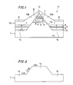
- a light-emitting diode 51 has a projecting portion 1a having a mesa-shape in a central area of a surface of a substrate 1.
- the substrate 1 is a semi-insulating substrate, the material for the substrate 1 is not limited thereto.
- An n-type buffer layer 2 is formed on a flat face of the projecting portion 1a of the substrate 1 and on flat surfaces of lower side areas 1b on both sides of the projecting portion 1a.
- an n-type first cladding layer 3 is formed on the n-type buffer layer 2.
- An undoped active layer 4 is formed on the n-type first cladding layer 3.
- a p-type second cladding layer 5 is formed on the undoped active layer 4.
- the n-type buffer layer 2, the n-type first cladding layer 3, the undoped active layer 4, and the p-type second cladding layer 5 constitute a doublehetero layer.
- a burying semiconductor layer 10 is formed on the layer 5 above the lower side areas 1 b so as to cover the side faces of the layers 2 to 5 above the projecting portion 1a and to cover the entire surface of the substrate 1.
- the burying semiconductor layer 10 is divided into two parts by the ridge of the layers 2 to 5 on the projecting portion la: the right part shown in Figure 1 is an n-type burying semiconductor layer 10a; and the left part is a p-type burying semiconductor layer 10b.
- the burying semiconductor layer 10 can be formed by a single growth step using the selective growth technique with the light excitation. Electrodes 8 and 9 are formed on the n-type burying semiconductor layer 10a and the p-type burying semiconductor layer 10b above the lower side areas 1b, respectively.
- the buffer layer 2 is formed of n-type GaAs to have a thickness of 0.2 ⁇ m.
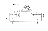
- each of the layers 2 to 5 on the projecting portion 1a is grown while forming the (111)B planes un- derthe growth conditions described above, the layers 2 to 5 are formed into a triangular shape in which the upper layer has a smaller area than that of the lower layer along the side slopes of the projecting portion 1a, as shown in Figure 3. Therefore, the width of the projecting portion 1a should be set so that the ridge of the triangle can be formed when the uppermost layer, i.e., the second cladding layer 5, is formed to have a predetermined thickness.
- Each of the layers 2 to 5 is formed on the lower side area 1b along the side slope of the projecting portion la so that the upper layer is wider than the lower layer.
- the layers 2 to 5 are not grown on the side slopes. Since the difference in level of the projecting portion 1a is about 5 ⁇ m, the second cladding layer 5, which is the uppermost layer formed on the lower side area 1 b, is lower than the flat portion of the projecting portion 1a, thereby exposing the side slopes of the projecting portion 1a by 1 ⁇ m or more.
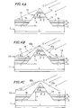
- the burying semiconductor layer 10 is formed by MOCVD with the light excitation as shown in Figures 4A through 4C.
- the burying semiconductor layer 10 is formed of AIGalnP having the same composition ratio as that of the current blocking layer 106 shown in Figure 12.
- the projecting portion 1a and the lower side areas 1b are connected by the growth of a (311) plane.
- the burying semiconductor layer 10 is formed so as to cover the entire surface of the substrate 1.
- the burying semiconductor layer 10 is formed so as to have thicknesses of, for example, 3 ⁇ m on the flat area and 1.5 ⁇ m in the vicinity of the ridge.
- the laser light (excitation light) is radiated at an angle (not at a right angle) with respect to the surface of the substrate 1 as indicated by the arrows C with solid lines shown in Figure 4A.
- the intensity of the laser light and the peak output can be set in the range, for example, from 100 to 400 joules (J) per pulse and from 10 to 40 megawatts (MW), respectively.
- the laser light having a wavelength of 248.5 nanometers (nm) or 249.5 nm is herein applied.
- the laser light having such wavelength and intensity can be obtained, for example, by a KrF excimer laser apparatus.
- the incident angle 0 is obtained to be 3.8°.
- the mask 32 for selective excitation and the optical system apparatus 33 for focusing the pattern of the mask 32 are not required.
- the same group III organic gases, the group V hydride gases, and the dopants as those used in the conventional example are used and supplied to the vapor phase epitaxy apparatus.
- the left part from the ridge of the layers 2 to 5 on the projecting portion 1a is not exposed to the laser light. More specifically, since the surface 11 of the cladding layer 5 is on the right side, the surface 11 is exposed to the laser light. On the other hand, since the surface 12 of the cladding layer 5 is on the left side, the laser light is prevented from being radiated thereon, whereby the surface 12 is shaded. Moreover, since the slope 13 of the layers 2 to 5 on the projecting portion 1a is on the right side, the laser light is radiated thereon. On the other hand, as being on the left side, the slope 14 is not exposed to the light.
- Figure 4C shows the terminal point of the growth of the burying semiconductor layer 10. As shown in the figure, when the burying semiconductor layer 10 on the ridge has a thickness of about 1.5 ⁇ m, the ridge area is flattened. The burying semiconductor layer 10b is completed under the condition that the laser light is not radiated thereon.
- the burying semiconductor layer 10a made of (Al 0.7 Ga 0.3 ) 0.5 In 0.5 P having an n-type conductivity with the impurity concentration of 5 x 10 17 / CM 3 is formed.
- the burying semiconductor layer 10b made of (Al 0.7 Ga 0.3 ) 0.5 In 0.5 P having a p-type conductivity with the impurity concentration of 3 x 10 17 /cm 3 is formed.
- the two layers having different compositions can be formed by a single vapor phase epitaxy step without a mask.
- the light-emitting diode 51 when the voltage is applied to the electrodes 8 and 9, the current does not flow through the layers 2 to 5 on the lower side area 1a as shown in Figure 1 since the substrate 1 is a semi-insulating substrate. As a result, the injected current Ip is injected into the active layer 4 on the projecting portion 1a alone. Since the light generated in the active layer 4 is emitted through an emitting surface of the projecting portion as indicated by the arrows B of the solid lines, the total reflection is reduced as compared with the case where the emitting surface is flat, thereby improving the external light emitting efficiency by one or more orders. More specifically, in the case where the light-emitting diode of Example 1 is molded using a resin to have a diameter of 5 mm, the light intensity of 3 candela can be obtained while the current of 20 mA is passed.
- PN junctions indicated by thick lines are formed between the burying semiconductor layers 10b and 10a, the burying layer 10a and the second cladding layer 5 above the projecting portion 1a, and the burying layer 10b and the first cladding layer 3 above the projecting portion 1a, respectively. These three PN junctions, however, do not function so as to prevent the current from flowing into the active layer 4 formed on the projecting portion 1a.
- Figure 7 is a vertical cross-sectional view showing a configuration for a light-emitting diode so as to illustrate Example 2 of the present invention.
- components having the same functions as those of Example 1 shown in Figure 1 are indicated by the same reference numerals, and the descriptions thereof are omitted.
- Example 2 the projecting portion 1a on the substrate 1 shown in Example 1 is formed into a reverse mesa-shape. More specifically, the projecting portion having a reverse mesa-shape is formed by etching in a [0-11] direction with respect to the (100) plane of both sides with a mask on the central area of the surface of the substrate 1.
- the layers 2 to 5 and the burying semiconductor layer 10 and the like can be formed in the same manner as that of Example 1.
- the current is applied to the electrodes 8 and 9
- the current is injected with high current efficiency as indicated by the arrows of broken lines D shown in Figure 7 and the light generated in the active layer 4 is emitted from the emitting surface of the projecting portion 1a as indicated by the arrows E with solid lines.
- the emitted light can be obtained with high efficiency, thereby obtaining the same effects as those in Example 1.
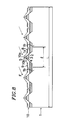
- Figures 8 and 9 show Example 3 of the present invention.
- Figure 8 is a vertical cross-sectional view showing a configuration for a light-emitting diode
- Figure 9 is a plan view showing a wiring pattern of the electrodes of the light-emitting diode.
- components having the same functions as those of Example 1 shown in Figure 1 are indicated by the same reference numerals, and the descriptions thereof are omitted.
- the incident angle 0 of the laser light for the formation of the semiconductor substrate 10 is proportional to the difference in level h between the projecting portion 1a and the lower side area 1b as indicated by Equation (1) described above.
- the incident angle 0 results in a small value, for example, 3.8° obtained in Example 1.
- the length L of the device region is divided by providing a plurality of the projecting portions 1a. Therefore, it is possible to radiate the laser light indicated by the arrows with solid lines F shown in Figure 8 at a large angle 0. Namely, if n projecting portions are provided at regular intervals in the device region, the length f of each light emitting region is obtained to be L/n.
- the incident angle 0 of this case is obtained by the following Equation (2):
- Example 3 since the current should be injected into the active layer 4 on each projecting portion 1a, it is necessary to provide the electrodes 8 and 9 for each projecting portion 1a. Therefore, the electrodes 8 and 9 are formed in a combination to have a comb-like shape on the burying semiconductor layer 10 as shown in Figure 9 so that the current is injected into the plurality of light emitting regions with high efficiency.
- the light intensity of 4 candela is obtained at a wavelength of 555 nm by the light-emitting diode of the present invention.
- semiconductor substrates having a projecting portion are used in the preceding examples, it will be appreciated that semiconductor substrates having other three-dimensional shapes which can shade a predetermined portion by the irradiation of light may alternatively be used.
- Other three-dimensional shapes such as a cylindrical shape, a trigonal pyramid, and a cone projecting on the surface of the substrate can also be used.
- a concave portion may be formed on the surface of the substrate, so that light is radiated at an angle with respect to the surface of the semiconductor substrate so as to prevent the light from being radiated on the bottom face of the concave portion, thereby growing the semiconductor layers.
- Figure 10 is a sectional view for illustrating a method for forming a conductive layer on a substrate 40 having a step 41 thereon.
- Semiconductor layers 43, 44, and 45 can be formed by the vapor phase epitaxy, radiating light 42 at an angle 0 with respect to the surface of the substrate 40.
- the semiconductor layers 43 and 44 formed of (Al 0.7 Ga 0.3 ) 0.5 In 0.5 P having an n-type conductivity with an impurity concentrations of 5 x 10 17 /cm 3 and the semiconductor layer 45 formed of (Al 0.7 Ga 0.3 ) 0.5 In 0.5 P having a p-type conductivity with an impurity concentrations of 3 x 10 17 /cm a are formed.
Landscapes
- Chemical & Material Sciences (AREA)
- Health & Medical Sciences (AREA)
- Toxicology (AREA)
- General Chemical & Material Sciences (AREA)
- Chemical Kinetics & Catalysis (AREA)
- Engineering & Computer Science (AREA)
- Materials Engineering (AREA)
- Mechanical Engineering (AREA)
- Metallurgy (AREA)
- Organic Chemistry (AREA)
- Led Devices (AREA)
Applications Claiming Priority (3)
| Application Number | Priority Date | Filing Date | Title |
|---|---|---|---|
| JP19049793A JP2960838B2 (ja) | 1993-07-30 | 1993-07-30 | 半導体装置及びその製造方法 |
| JP190497/93 | 1993-07-30 | ||
| JP19049793 | 1993-07-30 |
Publications (3)
| Publication Number | Publication Date |
|---|---|
| EP0637086A2 true EP0637086A2 (de) | 1995-02-01 |
| EP0637086A3 EP0637086A3 (de) | 1996-03-06 |
| EP0637086B1 EP0637086B1 (de) | 2003-04-09 |
Family
ID=16259081
Family Applications (1)
| Application Number | Title | Priority Date | Filing Date |
|---|---|---|---|
| EP94305613A Expired - Lifetime EP0637086B1 (de) | 1993-07-30 | 1994-07-28 | Lichtemittierendes Halbleiterbauelement und lichtunterstütztes Abscheideverfahren zu seiner Herstellung |
Country Status (4)
| Country | Link |
|---|---|
| US (2) | US5581116A (de) |
| EP (1) | EP0637086B1 (de) |
| JP (1) | JP2960838B2 (de) |
| DE (1) | DE69432446T2 (de) |
Cited By (2)
| Publication number | Priority date | Publication date | Assignee | Title |
|---|---|---|---|---|
| EP2174358A4 (de) * | 2007-07-27 | 2010-07-28 | Lg Innotek Co Ltd | Lichtemittierendes halbleiterelement und verfahren zu seiner herstellung |
| EP2221886A3 (de) * | 2009-02-18 | 2013-10-09 | LG Innotek Co., Ltd. | Lichtemittierendes Halbleiter-Bauelement |
Families Citing this family (8)
| Publication number | Priority date | Publication date | Assignee | Title |
|---|---|---|---|---|
| US6552712B1 (en) * | 1997-06-11 | 2003-04-22 | Seiko Epson Corporation | Semiconductor device, liquid crystal display, and electronic equipment including the same |
| JP4164438B2 (ja) * | 2003-11-12 | 2008-10-15 | 株式会社日立製作所 | 半導体光素子の製造方法 |
| US7982205B2 (en) * | 2006-01-12 | 2011-07-19 | National Institute Of Advanced Industrial Science And Technology | III-V group compound semiconductor light-emitting diode |
| JP5211728B2 (ja) * | 2007-02-07 | 2013-06-12 | 住友電気工業株式会社 | 半導体光素子を作製する方法 |
| JP5186852B2 (ja) * | 2007-09-14 | 2013-04-24 | ソニー株式会社 | 半導体発光素子 |
| JP2009071172A (ja) * | 2007-09-14 | 2009-04-02 | Sony Corp | 半導体発光素子及びその製造方法、並びに、下地層の形成方法 |
| DE102015104206A1 (de) * | 2015-03-20 | 2016-09-22 | Osram Opto Semiconductors Gmbh | Laserdiode |
| KR102748974B1 (ko) * | 2019-06-21 | 2025-01-03 | 삼성디스플레이 주식회사 | 표시 장치 및 그의 제조 방법 |
Family Cites Families (10)
| Publication number | Priority date | Publication date | Assignee | Title |
|---|---|---|---|---|
| JPH0632331B2 (ja) * | 1984-08-08 | 1994-04-27 | 松下電器産業株式会社 | 半導体レ−ザ装置およびその製造方法 |
| GB8516853D0 (en) * | 1985-07-03 | 1985-08-07 | British Telecomm | Manufacture of semiconductor structures |
| JPS63244625A (ja) * | 1987-03-30 | 1988-10-12 | Fujitsu Ltd | 半導体装置の製造方法 |
| US4956682A (en) * | 1987-04-28 | 1990-09-11 | Matsushita Electric Industrial Co., Ltd. | Optoelectronic integrated circuit |
| JPH01149426A (ja) * | 1987-12-04 | 1989-06-12 | Fujitsu Ltd | 半導体装置の製造方法 |
| US5202285A (en) * | 1990-04-26 | 1993-04-13 | Fujitsu Limited | Semiconductor laser having double heterostructure and method of producing same |
| JPH04352374A (ja) * | 1991-05-29 | 1992-12-07 | Eastman Kodak Japan Kk | 半導体発光装置 |
| EP0533197A3 (en) * | 1991-09-20 | 1993-11-03 | Fujitsu Ltd | Stripe laser diode having an improved efficiency for current confinement |
| JP2856374B2 (ja) * | 1992-02-24 | 1999-02-10 | シャープ株式会社 | 半導体発光素子及びその製造方法 |
| US5373173A (en) * | 1992-05-20 | 1994-12-13 | Sony Corporation | Apparatus for semiconductor laser |
-
1993
- 1993-07-30 JP JP19049793A patent/JP2960838B2/ja not_active Expired - Fee Related
-
1994
- 1994-07-28 US US08/281,834 patent/US5581116A/en not_active Expired - Lifetime
- 1994-07-28 EP EP94305613A patent/EP0637086B1/de not_active Expired - Lifetime
- 1994-07-28 DE DE69432446T patent/DE69432446T2/de not_active Expired - Fee Related
-
1996
- 1996-06-28 US US08/673,263 patent/US5854089A/en not_active Expired - Fee Related
Cited By (3)
| Publication number | Priority date | Publication date | Assignee | Title |
|---|---|---|---|---|
| EP2174358A4 (de) * | 2007-07-27 | 2010-07-28 | Lg Innotek Co Ltd | Lichtemittierendes halbleiterelement und verfahren zu seiner herstellung |
| US7875874B2 (en) | 2007-07-27 | 2011-01-25 | Lg Innotek Co., Ltd. | Semiconductor light emitting device and method of manufacturing the same |
| EP2221886A3 (de) * | 2009-02-18 | 2013-10-09 | LG Innotek Co., Ltd. | Lichtemittierendes Halbleiter-Bauelement |
Also Published As
| Publication number | Publication date |
|---|---|
| JP2960838B2 (ja) | 1999-10-12 |
| DE69432446D1 (de) | 2003-05-15 |
| EP0637086A3 (de) | 1996-03-06 |
| DE69432446T2 (de) | 2004-01-15 |
| US5854089A (en) | 1998-12-29 |
| EP0637086B1 (de) | 2003-04-09 |
| US5581116A (en) | 1996-12-03 |
| JPH0745865A (ja) | 1995-02-14 |
Similar Documents
| Publication | Publication Date | Title |
|---|---|---|
| US6841409B2 (en) | Group III-V compound semiconductor and group III-V compound semiconductor device using the same | |
| US5872022A (en) | Method for etching a semiconductor method for fabricating semiconductor device method for fabricating semiconductor laser and semiconductor laser | |
| US5469457A (en) | Semiconductor laser with COD preventing disordered regions | |
| US5089437A (en) | Semiconductor laser manufacturing method | |
| US4922499A (en) | Semiconductor laser device and the manufacturing method thereof | |
| US6509579B2 (en) | Semiconductor device | |
| US4843031A (en) | Method of fabricating compound semiconductor laser using selective irradiation | |
| EP0430691A2 (de) | Halbleiter-Heterostrukturen | |
| EP0423535A2 (de) | Halbleiteranordnung hergestellt mittels einer epitaxialen Technik und Verfahren zur Herstellung dieser Anordnung | |
| EP0437243A2 (de) | Halbleiterlaser und Verfahren zu seiner Herstellung | |
| US5573976A (en) | Method of fabricating semiconductor laser | |
| US5581116A (en) | Semiconductor device manufactured by selectively controlling growth of an epitaxial layer without a mask | |
| EP1265326B1 (de) | Dfb-halbleiterlaserbauelement mit verstärkungs-kopplung und verfahren zu seiner herstellung | |
| JP3432909B2 (ja) | 半導体レーザ | |
| EP0473443B1 (de) | Halbleiterlaser mit vergrabener Streifenstruktur | |
| JP3206080B2 (ja) | 半導体レーザ | |
| JPH0786630A (ja) | 単一波長受光素子 | |
| US5518954A (en) | Method for fabricating a semiconductor laser | |
| EP0432843B1 (de) | Halbleiterdiodenlaser und Verfahren zur Herstellung desselben | |
| US5278857A (en) | Indium gallium aluminum phosphide silicon doped to prevent zinc disordering | |
| KR0141057B1 (ko) | 반도체 레이저 제조방법 | |
| JP3257254B2 (ja) | 化合物半導体素子及びその作製方法 | |
| US7046708B2 (en) | Semiconductor laser device including cladding layer having stripe portion different in conductivity type from adjacent portions | |
| JPH05226781A (ja) | 半導体発光素子の製造方法 | |
| KR100275771B1 (ko) | 반도체 레이저 소자 및 그의 제조 방법 |
Legal Events
| Date | Code | Title | Description |
|---|---|---|---|
| PUAI | Public reference made under article 153(3) epc to a published international application that has entered the european phase |
Free format text: ORIGINAL CODE: 0009012 |
|
| AK | Designated contracting states |
Kind code of ref document: A2 Designated state(s): DE FR GB |
|
| PUAL | Search report despatched |
Free format text: ORIGINAL CODE: 0009013 |
|
| AK | Designated contracting states |
Kind code of ref document: A3 Designated state(s): DE FR GB |
|
| 17P | Request for examination filed |
Effective date: 19960610 |
|
| 17Q | First examination report despatched |
Effective date: 19970417 |
|
| GRAG | Despatch of communication of intention to grant |
Free format text: ORIGINAL CODE: EPIDOS AGRA |
|
| GRAG | Despatch of communication of intention to grant |
Free format text: ORIGINAL CODE: EPIDOS AGRA |
|
| GRAH | Despatch of communication of intention to grant a patent |
Free format text: ORIGINAL CODE: EPIDOS IGRA |
|
| GRAH | Despatch of communication of intention to grant a patent |
Free format text: ORIGINAL CODE: EPIDOS IGRA |
|
| GRAA | (expected) grant |
Free format text: ORIGINAL CODE: 0009210 |
|
| AK | Designated contracting states |
Designated state(s): DE FR GB |
|
| REG | Reference to a national code |
Ref country code: GB Ref legal event code: FG4D |
|
| ET | Fr: translation filed | ||
| PLBE | No opposition filed within time limit |
Free format text: ORIGINAL CODE: 0009261 |
|
| STAA | Information on the status of an ep patent application or granted ep patent |
Free format text: STATUS: NO OPPOSITION FILED WITHIN TIME LIMIT |
|
| 26N | No opposition filed |
Effective date: 20040112 |
|
| PGFP | Annual fee paid to national office [announced via postgrant information from national office to epo] |
Ref country code: DE Payment date: 20080807 Year of fee payment: 15 |
|
| PGFP | Annual fee paid to national office [announced via postgrant information from national office to epo] |
Ref country code: FR Payment date: 20080718 Year of fee payment: 15 |
|
| PGFP | Annual fee paid to national office [announced via postgrant information from national office to epo] |
Ref country code: GB Payment date: 20080806 Year of fee payment: 15 |
|
| GBPC | Gb: european patent ceased through non-payment of renewal fee |
Effective date: 20090728 |
|
| REG | Reference to a national code |
Ref country code: FR Ref legal event code: ST Effective date: 20100331 |
|
| PG25 | Lapsed in a contracting state [announced via postgrant information from national office to epo] |
Ref country code: FR Free format text: LAPSE BECAUSE OF NON-PAYMENT OF DUE FEES Effective date: 20090731 |
|
| PG25 | Lapsed in a contracting state [announced via postgrant information from national office to epo] |
Ref country code: GB Free format text: LAPSE BECAUSE OF NON-PAYMENT OF DUE FEES Effective date: 20090728 |
|
| PG25 | Lapsed in a contracting state [announced via postgrant information from national office to epo] |
Ref country code: DE Free format text: LAPSE BECAUSE OF NON-PAYMENT OF DUE FEES Effective date: 20100202 |