EP0423535A2 - Halbleiteranordnung hergestellt mittels einer epitaxialen Technik und Verfahren zur Herstellung dieser Anordnung - Google Patents
Halbleiteranordnung hergestellt mittels einer epitaxialen Technik und Verfahren zur Herstellung dieser Anordnung Download PDFInfo
- Publication number
- EP0423535A2 EP0423535A2 EP90118867A EP90118867A EP0423535A2 EP 0423535 A2 EP0423535 A2 EP 0423535A2 EP 90118867 A EP90118867 A EP 90118867A EP 90118867 A EP90118867 A EP 90118867A EP 0423535 A2 EP0423535 A2 EP 0423535A2
- Authority
- EP
- European Patent Office
- Prior art keywords
- layers
- type
- layer
- substrate
- areas
- Prior art date
- Legal status (The legal status is an assumption and is not a legal conclusion. Google has not performed a legal analysis and makes no representation as to the accuracy of the status listed.)
- Granted
Links
Images



Classifications
-
- G—PHYSICS
- G02—OPTICS
- G02B—OPTICAL ELEMENTS, SYSTEMS OR APPARATUS
- G02B6/00—Light guides; Structural details of arrangements comprising light guides and other optical elements, e.g. couplings
- G02B6/10—Light guides; Structural details of arrangements comprising light guides and other optical elements, e.g. couplings of the optical waveguide type
- G02B6/12—Light guides; Structural details of arrangements comprising light guides and other optical elements, e.g. couplings of the optical waveguide type of the integrated circuit kind
- G02B6/13—Integrated optical circuits characterised by the manufacturing method
- G02B6/131—Integrated optical circuits characterised by the manufacturing method by using epitaxial growth
-
- H—ELECTRICITY
- H10—SEMICONDUCTOR DEVICES; ELECTRIC SOLID-STATE DEVICES NOT OTHERWISE PROVIDED FOR
- H10H—INORGANIC LIGHT-EMITTING SEMICONDUCTOR DEVICES HAVING POTENTIAL BARRIERS
- H10H20/00—Individual inorganic light-emitting semiconductor devices having potential barriers, e.g. light-emitting diodes [LED]
- H10H20/01—Manufacture or treatment
- H10H20/011—Manufacture or treatment of bodies, e.g. forming semiconductor layers
- H10H20/013—Manufacture or treatment of bodies, e.g. forming semiconductor layers having light-emitting regions comprising only Group III-V materials
-
- H—ELECTRICITY
- H01—ELECTRIC ELEMENTS
- H01S—DEVICES USING THE PROCESS OF LIGHT AMPLIFICATION BY STIMULATED EMISSION OF RADIATION [LASER] TO AMPLIFY OR GENERATE LIGHT; DEVICES USING STIMULATED EMISSION OF ELECTROMAGNETIC RADIATION IN WAVE RANGES OTHER THAN OPTICAL
- H01S5/00—Semiconductor lasers
- H01S5/10—Construction or shape of the optical resonator, e.g. extended or external cavity, coupled cavities, bent-guide, varying width, thickness or composition of the active region
- H01S5/16—Window-type lasers, i.e. with a region of non-absorbing material between the active region and the reflecting surface
-
- H—ELECTRICITY
- H01—ELECTRIC ELEMENTS
- H01S—DEVICES USING THE PROCESS OF LIGHT AMPLIFICATION BY STIMULATED EMISSION OF RADIATION [LASER] TO AMPLIFY OR GENERATE LIGHT; DEVICES USING STIMULATED EMISSION OF ELECTROMAGNETIC RADIATION IN WAVE RANGES OTHER THAN OPTICAL
- H01S5/00—Semiconductor lasers
- H01S5/20—Structure or shape of the semiconductor body to guide the optical wave ; Confining structures perpendicular to the optical axis, e.g. index or gain guiding, stripe geometry, broad area lasers, gain tailoring, transverse or lateral reflectors, special cladding structures, MQW barrier reflection layers
- H01S5/22—Structure or shape of the semiconductor body to guide the optical wave ; Confining structures perpendicular to the optical axis, e.g. index or gain guiding, stripe geometry, broad area lasers, gain tailoring, transverse or lateral reflectors, special cladding structures, MQW barrier reflection layers having a ridge or stripe structure
- H01S5/227—Buried mesa structure ; Striped active layer
-
- H—ELECTRICITY
- H10—SEMICONDUCTOR DEVICES; ELECTRIC SOLID-STATE DEVICES NOT OTHERWISE PROVIDED FOR
- H10H—INORGANIC LIGHT-EMITTING SEMICONDUCTOR DEVICES HAVING POTENTIAL BARRIERS
- H10H20/00—Individual inorganic light-emitting semiconductor devices having potential barriers, e.g. light-emitting diodes [LED]
- H10H20/01—Manufacture or treatment
-
- H—ELECTRICITY
- H10—SEMICONDUCTOR DEVICES; ELECTRIC SOLID-STATE DEVICES NOT OTHERWISE PROVIDED FOR
- H10P—GENERIC PROCESSES OR APPARATUS FOR THE MANUFACTURE OR TREATMENT OF DEVICES COVERED BY CLASS H10
- H10P14/00—Formation of materials, e.g. in the shape of layers or pillars
- H10P14/20—Formation of materials, e.g. in the shape of layers or pillars of semiconductor materials
- H10P14/27—Formation of materials, e.g. in the shape of layers or pillars of semiconductor materials using selective deposition, e.g. simultaneous growth of monocrystalline and non-monocrystalline semiconductor materials
- H10P14/271—Formation of materials, e.g. in the shape of layers or pillars of semiconductor materials using selective deposition, e.g. simultaneous growth of monocrystalline and non-monocrystalline semiconductor materials characterised by the preparation of substrate for selective deposition
-
- H—ELECTRICITY
- H10—SEMICONDUCTOR DEVICES; ELECTRIC SOLID-STATE DEVICES NOT OTHERWISE PROVIDED FOR
- H10P—GENERIC PROCESSES OR APPARATUS FOR THE MANUFACTURE OR TREATMENT OF DEVICES COVERED BY CLASS H10
- H10P14/00—Formation of materials, e.g. in the shape of layers or pillars
- H10P14/20—Formation of materials, e.g. in the shape of layers or pillars of semiconductor materials
- H10P14/29—Formation of materials, e.g. in the shape of layers or pillars of semiconductor materials characterised by the substrates
- H10P14/2901—Materials
-
- H—ELECTRICITY
- H10—SEMICONDUCTOR DEVICES; ELECTRIC SOLID-STATE DEVICES NOT OTHERWISE PROVIDED FOR
- H10P—GENERIC PROCESSES OR APPARATUS FOR THE MANUFACTURE OR TREATMENT OF DEVICES COVERED BY CLASS H10
- H10P14/00—Formation of materials, e.g. in the shape of layers or pillars
- H10P14/20—Formation of materials, e.g. in the shape of layers or pillars of semiconductor materials
- H10P14/29—Formation of materials, e.g. in the shape of layers or pillars of semiconductor materials characterised by the substrates
- H10P14/2901—Materials
- H10P14/2907—Materials being Group IIIA-VA materials
- H10P14/2911—Arsenides
-
- H—ELECTRICITY
- H10—SEMICONDUCTOR DEVICES; ELECTRIC SOLID-STATE DEVICES NOT OTHERWISE PROVIDED FOR
- H10P—GENERIC PROCESSES OR APPARATUS FOR THE MANUFACTURE OR TREATMENT OF DEVICES COVERED BY CLASS H10
- H10P14/00—Formation of materials, e.g. in the shape of layers or pillars
- H10P14/20—Formation of materials, e.g. in the shape of layers or pillars of semiconductor materials
- H10P14/32—Formation of materials, e.g. in the shape of layers or pillars of semiconductor materials characterised by intermediate layers between substrates and deposited layers
- H10P14/3202—Materials thereof
- H10P14/3214—Materials thereof being Group IIIA-VA semiconductors
- H10P14/3218—Phosphides
-
- H—ELECTRICITY
- H10—SEMICONDUCTOR DEVICES; ELECTRIC SOLID-STATE DEVICES NOT OTHERWISE PROVIDED FOR
- H10P—GENERIC PROCESSES OR APPARATUS FOR THE MANUFACTURE OR TREATMENT OF DEVICES COVERED BY CLASS H10
- H10P14/00—Formation of materials, e.g. in the shape of layers or pillars
- H10P14/20—Formation of materials, e.g. in the shape of layers or pillars of semiconductor materials
- H10P14/32—Formation of materials, e.g. in the shape of layers or pillars of semiconductor materials characterised by intermediate layers between substrates and deposited layers
- H10P14/3202—Materials thereof
- H10P14/3214—Materials thereof being Group IIIA-VA semiconductors
- H10P14/3221—Arsenides
-
- H—ELECTRICITY
- H10—SEMICONDUCTOR DEVICES; ELECTRIC SOLID-STATE DEVICES NOT OTHERWISE PROVIDED FOR
- H10P—GENERIC PROCESSES OR APPARATUS FOR THE MANUFACTURE OR TREATMENT OF DEVICES COVERED BY CLASS H10
- H10P14/00—Formation of materials, e.g. in the shape of layers or pillars
- H10P14/20—Formation of materials, e.g. in the shape of layers or pillars of semiconductor materials
- H10P14/32—Formation of materials, e.g. in the shape of layers or pillars of semiconductor materials characterised by intermediate layers between substrates and deposited layers
- H10P14/3202—Materials thereof
- H10P14/3224—Materials thereof being Group IIB-VIA semiconductors
- H10P14/3231—Selenides
-
- H—ELECTRICITY
- H10—SEMICONDUCTOR DEVICES; ELECTRIC SOLID-STATE DEVICES NOT OTHERWISE PROVIDED FOR
- H10P—GENERIC PROCESSES OR APPARATUS FOR THE MANUFACTURE OR TREATMENT OF DEVICES COVERED BY CLASS H10
- H10P14/00—Formation of materials, e.g. in the shape of layers or pillars
- H10P14/20—Formation of materials, e.g. in the shape of layers or pillars of semiconductor materials
- H10P14/34—Deposited materials, e.g. layers
- H10P14/3402—Deposited materials, e.g. layers characterised by the chemical composition
- H10P14/3414—Deposited materials, e.g. layers characterised by the chemical composition being group IIIA-VIA materials
- H10P14/3418—Phosphides
-
- H—ELECTRICITY
- H10—SEMICONDUCTOR DEVICES; ELECTRIC SOLID-STATE DEVICES NOT OTHERWISE PROVIDED FOR
- H10P—GENERIC PROCESSES OR APPARATUS FOR THE MANUFACTURE OR TREATMENT OF DEVICES COVERED BY CLASS H10
- H10P14/00—Formation of materials, e.g. in the shape of layers or pillars
- H10P14/20—Formation of materials, e.g. in the shape of layers or pillars of semiconductor materials
- H10P14/34—Deposited materials, e.g. layers
- H10P14/3402—Deposited materials, e.g. layers characterised by the chemical composition
- H10P14/3414—Deposited materials, e.g. layers characterised by the chemical composition being group IIIA-VIA materials
- H10P14/3421—Arsenides
-
- H—ELECTRICITY
- H01—ELECTRIC ELEMENTS
- H01S—DEVICES USING THE PROCESS OF LIGHT AMPLIFICATION BY STIMULATED EMISSION OF RADIATION [LASER] TO AMPLIFY OR GENERATE LIGHT; DEVICES USING STIMULATED EMISSION OF ELECTROMAGNETIC RADIATION IN WAVE RANGES OTHER THAN OPTICAL
- H01S5/00—Semiconductor lasers
- H01S5/20—Structure or shape of the semiconductor body to guide the optical wave ; Confining structures perpendicular to the optical axis, e.g. index or gain guiding, stripe geometry, broad area lasers, gain tailoring, transverse or lateral reflectors, special cladding structures, MQW barrier reflection layers
- H01S5/22—Structure or shape of the semiconductor body to guide the optical wave ; Confining structures perpendicular to the optical axis, e.g. index or gain guiding, stripe geometry, broad area lasers, gain tailoring, transverse or lateral reflectors, special cladding structures, MQW barrier reflection layers having a ridge or stripe structure
- H01S5/223—Buried stripe structure
- H01S5/2232—Buried stripe structure with inner confining structure between the active layer and the lower electrode
-
- H—ELECTRICITY
- H01—ELECTRIC ELEMENTS
- H01S—DEVICES USING THE PROCESS OF LIGHT AMPLIFICATION BY STIMULATED EMISSION OF RADIATION [LASER] TO AMPLIFY OR GENERATE LIGHT; DEVICES USING STIMULATED EMISSION OF ELECTROMAGNETIC RADIATION IN WAVE RANGES OTHER THAN OPTICAL
- H01S5/00—Semiconductor lasers
- H01S5/20—Structure or shape of the semiconductor body to guide the optical wave ; Confining structures perpendicular to the optical axis, e.g. index or gain guiding, stripe geometry, broad area lasers, gain tailoring, transverse or lateral reflectors, special cladding structures, MQW barrier reflection layers
- H01S5/22—Structure or shape of the semiconductor body to guide the optical wave ; Confining structures perpendicular to the optical axis, e.g. index or gain guiding, stripe geometry, broad area lasers, gain tailoring, transverse or lateral reflectors, special cladding structures, MQW barrier reflection layers having a ridge or stripe structure
- H01S5/227—Buried mesa structure ; Striped active layer
- H01S5/2272—Buried mesa structure ; Striped active layer grown by a mask induced selective growth
-
- H—ELECTRICITY
- H01—ELECTRIC ELEMENTS
- H01S—DEVICES USING THE PROCESS OF LIGHT AMPLIFICATION BY STIMULATED EMISSION OF RADIATION [LASER] TO AMPLIFY OR GENERATE LIGHT; DEVICES USING STIMULATED EMISSION OF ELECTROMAGNETIC RADIATION IN WAVE RANGES OTHER THAN OPTICAL
- H01S5/00—Semiconductor lasers
- H01S5/20—Structure or shape of the semiconductor body to guide the optical wave ; Confining structures perpendicular to the optical axis, e.g. index or gain guiding, stripe geometry, broad area lasers, gain tailoring, transverse or lateral reflectors, special cladding structures, MQW barrier reflection layers
- H01S5/22—Structure or shape of the semiconductor body to guide the optical wave ; Confining structures perpendicular to the optical axis, e.g. index or gain guiding, stripe geometry, broad area lasers, gain tailoring, transverse or lateral reflectors, special cladding structures, MQW barrier reflection layers having a ridge or stripe structure
- H01S5/227—Buried mesa structure ; Striped active layer
- H01S5/2275—Buried mesa structure ; Striped active layer mesa created by etching
-
- Y—GENERAL TAGGING OF NEW TECHNOLOGICAL DEVELOPMENTS; GENERAL TAGGING OF CROSS-SECTIONAL TECHNOLOGIES SPANNING OVER SEVERAL SECTIONS OF THE IPC; TECHNICAL SUBJECTS COVERED BY FORMER USPC CROSS-REFERENCE ART COLLECTIONS [XRACs] AND DIGESTS
- Y10—TECHNICAL SUBJECTS COVERED BY FORMER USPC
- Y10S—TECHNICAL SUBJECTS COVERED BY FORMER USPC CROSS-REFERENCE ART COLLECTIONS [XRACs] AND DIGESTS
- Y10S438/00—Semiconductor device manufacturing: process
- Y10S438/914—Doping
- Y10S438/925—Fluid growth doping control, e.g. delta doping
Definitions
- the present invention relates to a semiconductor device and a method for making the same, and in particular to a semiconductor device including one or more semiconductor layers formed as one or more functional layers on a semiconductor substrate and composed of a compound semiconductor and a method for making the same.
- the present invention is extensively employed for a functional device including an electronic device such as a diode and transistor, an optical device such as an LED, LD and optical waveguide, and a sensor.
- the technique for making a semiconductor layer or layers on a semiconductor substrate is broadly classified into a planer technique principally using the diffusion, ion implantation, oxidation, etc., and an epitaxial growth technique principally using a liquid phase epitaxy (LPE) and vapor phase epitaxy (VPE and CVD).
- LPE liquid phase epitaxy
- VPE and CVD vapor phase epitaxy
- the epitaxial growth technique is employed as a technique for forming semiconductor crystal or mixed crystal layers of a different composition on a semiconductor substrate.
- HBT hetero-bipolar transistor
- HEMT high electron mobility transistor
- LED light emitting diode
- LD laser diode
- PD photodiode
- optical waveguide optical waveguide
- the epitaxial growth technique incudes, in addition to a liquid phase epitaxy (LPE) method and vapor phase epitaxy (VPE) method using a halogen transport, a metalorganic vapor phase epitaxy (MOVPE) and a molecular beam epitaxy (MBE) method (including an MOMBE method), as capable of a greater material selectivity as well as ready making of a fine structure, an atomic layer epitaxy (ALE) method, a photochemical VPE method using light, as a decomposition energy for a material, in place of heat, and so on.
- LPE liquid phase epitaxy
- VPE vapor phase epitaxy
- MBE molecular beam epitaxy
- ALE atomic layer epitaxy
- a photochemical VPE method using light as a decomposition energy for a material, in place of heat, and so on.
- the conventional semiconductor process technique can readily deposit layers of a different composition on a semiconductor substrate in a direction vertical to the substrate surface, but it has been difficult to deposit layers having a different composition area in a direction parallel to the substrate surface.
- a semiconductor area acting as the optical waveguide is formed such that it is surrounded with a clad area of a lower refractive index than that of the semiconductor area.
- Figs. 1A to 1C are perspective views showing various forms of an optical waveguide formed on a semiconductor substrate.
- Fig. 1A is an example in which an optical conducting layer 2 is formed on a substrate 1 such that it is surrounded with cladding layers 3 in a direction parallel to the surface of the substrate.
- Fig. 1B is an example in which an optical conducting layer 2 is formed on a substrate 1 such that it is surrounded with upper and lower cladding layers 3, in a stacking fashion, in a direction vertical to the surface of the substrate 1.
- Fig. 1A is an example in which an optical conducting layer 2 is formed on a substrate 1 such that it is surrounded with upper and lower cladding layers 3, in a stacking fashion, in a direction vertical to the surface of the substrate 1.
- FIG. 1C is an example in which an optical conducting layer 2 and cladding layers 3′ are formed as one unit on the surface of a substrate 1 in a direction parallel to the surface of the substrate in which case the unit is sandwiched with cladding layers 3 in that vertical direction except for opposite end faces of the optical conducting layer 2.
- the structure as shown in Fig. 1C allows light to be conducted to the inner region of the optical conducting layer 2. It will be readily understood that the structure of Fig. 1C is composed of a combination of the structures of Figs. 1A and 1B.
- Fig. 1B can readily be made by an epitaxial growth technique for semiconductors, that is, a cladding layer 3, optical conducting layer 2 and cladding layer 3 are sequentially grown over a semiconductor substrate 1 by an epitaxial growth method, such as a liquid phase epitaxy (LPE) or vapor phase epitaxy (VPE). If, at this time, the thickness of these layers has to be exactly controlled on the order of a few ⁇ m or below, it is advantageous to employ a molecular beam epitaxy (MBE) or a metalorganic vapor phase epitaxy (MOVPE) method.
- MBE molecular beam epitaxy
- MOVPE metalorganic vapor phase epitaxy
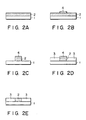
- Fig. 1A the structure of Fig. 1A is made as shown in Fig. 2. That is, an optical conducting layer 2 is grown as a crystal on a semiconductor substrate 1, by the epitaxial growth technique, as shown in Fig. 2A. Then a mask layer, such as an SiO2 film, is patterned, by a photoetching process (PEP), on the optical conducting layer 2 as shown in Fig. 2B and the optical conducting layer 2 is removed, by the etching process, at an area not covered with the mask 4 as shown in Fig. 2C. Cladding layers 3 are selectively grown, by the epitaxial growth technique, on the resultant exposed surface of the semiconductor substrate 1 as shown in Fig. 2C and, finally, the mask 4 on the optical conducting layer 2 is removed to expose the latter as shown in Fig. 2E.
- PEP photoetching process
- the problems as will be set forth below arise in the making of the optical waveguide shown in Fig. 2A.
- First the exposed side surfaces of the optical conducting layer 2 are injured or "side etched", by the etching process, during the making step as shown in Fig. 2C, or the exposed surfaces of the optical conducting layer are oxidized depending upon the material used at that process. It is, therefore, difficult to obtain a pure, exposed crystal face.
- discontinous surfaces are liable to be produced between the optical conducting layer and the cladding layer.
- discontinous surfaces and defects occur at the boundries between the optical conducting layer and the cladding layers 3, thus causing the absorption or scattering of light at the boundries of the optical waveguide.
- it is generally difficult to form an epitaxial layer, by a selective epitaxial growth method, on the surface of the mask and remaining surface of the resultant structure, as shown in Fig. 2D, and it is possible to perform such a selective epitaxial growth under the specific conditions only.
- the structure of the optical waveguide as shown in Fig. 1C is obtained by a combination of the process methods shown in Figs. 1A and 1B.
- a semiconductor device in which semiconductor layers are formed as functional layers on a semiconductor substrate in general, it is easier to sequentially form layers of different compositions on the semiconductor substrate in stacked fashion as shown in Fig. 1B, but it becomes very difficult to form such layers of different crystal compositions in a lateral direction, that is, in a direction parallel to a substrate surface as shown in Fig. 1A.
- the aforementioned wafer process often includes, for example, a selective etching and selective epitaxial growth process.
- the semiconductor layers as stacked in a complex process over the semiconductor substrate contain discontinuous surfaces or crystal defects which are liable to occur at the boundries between these layers of different crystal compositions. This is a cause for the degraded characteristics of a semiconductor device obtained.
- Another object of the present invention is to provide a laser diode which can readily form a window structure, by the aforementioned method, capable of suppressing a catastrophic optical damage (COD).
- COD catastrophic optical damage
- a method for making a semiconductor device in which semiconductor layers of a different band gap and/or a different composition are formed by an epitaxial growth technique on first and second areas formed adjacent the semiconductor surfaces, said method comprising the steps of: forming, adjacent a first area, a second area of a different composition or different electrical conduction, said first area being a portion of a major surface of a semiconductor substrate, to make the first and second area have a different surface temperature each at a heating step of a subsequent epitaxial growth process; and deposing, by the epitaxial growth technique on exposed surfaces of the first and second areas, compound semiconductor layers of a different band gap energy and/or a different composition each, while being lattice-matched to both the areas.
- a III-V ternary compound such as InGaP or a III-V quaternary compound such as InGaAlP is grown by a vapor phase growth method, such as an MOVPE, on a semiconductor substrate such as GaAs, a different crystal structure or different crystal composition layer is formed depending upon growth conditions, such as the growth temperature, growth pressure, doping and so on.
- Fig. 11 shows a growth temperature dependence, upon a band gap energy (Eg), of In 0.5 Ga 0.5 P grown as a crystal layer on a (100) GaAs substrate by an MOVPE method.
- Eg band gap energy
- the band gap energy (Ep) of In 0.5 Ga 0.5 P varies to an extent of about 0.05 eV at a growth temperature of 650°C to 750°C. Further, even if a feed supply rate is fixed in a crystal growth of InGaP, a resultant mixed crystal varies in composition depending upon the growth temperature, that is, the higher the growth temperature, the greater the value of In 1-x Ga x P and hence the band gap energy (Eg).
- Fig. 11 shows a variation of the band gap energy (Eg) for the same composition, that is, In 0.5 Ga 0.5 P, but an amount of variation of Eg against the growth temperature is further increased, considered together with an effect of a variation of the mixed crystal's composition by the growth temperature.
- Fig. 12 is a graph showing the temperature dependence of Eg for In 0.5 Ga 0.5 P actually prepared by a low pressure MOVPE method, the effect including a lattice mismatching effect resulting from the growth temperature.
- the band gap energy Eg is a value determined by a photoluminescence measurement.
- a semiconductor device according to a first embodiment of the present invention will be explained below in connection with an optical waveguide for instance.
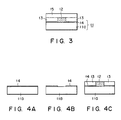
- Fig. 3 is cross-sectional view showing a modeled optical waveguide in the embodiment of the present invention.
- a semiconductor substrate 11 is composed of an n-type GaAs substrate 11a and crystal growth layer 14 formed on the substrate 11a at a given area.
- An optical conducting layer 12 is formed, as a first epitaxial layer of InGaP, on the exposed surface of an n type GaAs substrate at an area (first region) not covered with the crystal growth layer 14.
- Cladding layers 13 are formed, as second epitaxial layer of InGaP, on the exposed surface of the crystal growth layer (second area) 14.
- a cap layer 15 which is formed over the optical conducting layer 12 and cladding layers 13 is formed of a material, such as GaAlAs, GaAs, which can be grown without depending upon the surface temperature.
- the crystal growth layer 14 is formed of, for example, GaAlAs, InGaAlP or ZnSe, which is lattice-matched to GaAs and In 0.5 Ga 0.5 P, and can be formed as a thin insulating layer if a lattice matching is obtained.
- Fig. 4 is cross-sectional views showing making steps of an optical waveguide according to the first embodiment of the present invention.
- a thin InGaAlP crystal growth layer 14 of above 0.1 ⁇ m is formed by an MOVPE method on an n-type GaAs substrate 11a. Then the growth layer 14 is partially removed by a PEP technique to expose the GaAs substrate 11A at selected areas as shown in Fig. 4B.
- InGaP layers 12 and 13 are grown, as a crystal layer of 0.5 to a few ⁇ m thick, on the substrate, by virtue of the MOVPE method, under the same condition using a reaction gas at a feed supply rate In 0.5 /Ga 0.5 /P.
- the surface temperature of the crystal growth layer 14 becomes a higher level than that of the n type GaAs substrate 11a owing to a difference in composition between the n type GaAs substrate 11a and InGaAlP crystal growth layer 14.
- the surface temperature difference is maintained during the layer growth because an upper layer being grown is relatively thin.
- the layers 12 and 13 are grown over the semiconductor substrate under the same growth conductions, they are formed as growth layers of different Eg and crystal composition resulting from their surface temperature difference, that is, the InGaP layer 12 grown on the n type GaAs substrate 11a is made smaller in Eg, and greater in refractivity, than the layers 13 grown on the crystal growth layer 14.
- an epitaxial GaAlAs layer 15 is formed as a cap layer of a few ⁇ m to several tens of ⁇ m on the resultant structure by means of an MOVPE method to provide an optical waveguide as shown in Fig. 3.
- the present embodiment is directed to selectively forming a semiconductor layer on a substrate with their compositions made different from each other and forming upper semiconductor layers of different Eg and composition, utilizing a surface temperature difference between an area covered with the semiconductor layer and an area not covered with the semiconductor layer.
- Fig. 5 is a cross-sectional view showing a model of an optical waveguide according to a second embodiment of the present invention.
- an n-type GaAs substrate 31a has a mesa-like projection and GaAs crystal growth layers 34 of high resistance are buried in the mesa-like recess of the substrate.
- the crystal growth layer 34 may be of such a type as to have a high resistance layers or a different electric conductivity from that of a substrate 31a, such as p type GaAs, or is formed of a different material from that of a substrate 31a, such as GaAlAs, InGaAlP or ZnSe.
- a liquid phase epitaxy (LPE) method is employed to obtain a planarized substrate surface in which case it is desirable to use a material for LPE.
- First and second epitaxial layers 32 and 33 of InGaP are formed on the exposed surface of the substrate 31a and crystal growth layer 34, respectively.
- a cap layer 35 of GaAlAs (or GaAs) is formed on the epitaxial layers 32 and 33.
- Fig. 6 is cross-sectional views showing the making steps of an optical waveguide according to the second embodiment of the present invention.
- a mask 30, such as an SiO2 film is formed on the portion of an n type GaAs substrate 31a and, as shown in Fig. 6B, the GaAs substrate 31a is removed, by the PEP technique, at an area not covered with the mask 30, to an extent of about 0.5 to 1 ⁇ m to provide mesa-like recesses 36.
- high resistance GaAs layers 34 are buried, in the mesa-like recess, by a selective liquid phase epitaxy method, as shown in Fig. 6C.
- the layers 34 may be formed of GaAlAs, InGaAlP or ZnSe. Then the mask 30 is etched away as shown in Fig. 6D and InGaP layers 32 and 33 are grown, by the MOVPE method, on the resultant structure, as shown in Fig. 6E, under the same growth conditions using a reaction gas at a molar ratio In 0.5 /Ga 0.5 /P.
- the covered one is about 10° to 15°C higher in its surface temperature under the same conditions than the one not covered with the In 0.5 Ga 0.5 P layer.
- the exposed surface (first area) of the mesa-like substrate 31a is lower in its surface temperature than the grown crystal layers (second areas) 34. Therefore, the epitaxial layer 32 deposited on the exposed surface of the substrate 31a is made lower in Eg, and greater in light refractive index, than the epitaxial layers 33 deposited on the exposed surface of the crystal growth layer 34.
- cap layer 35 of GaAlAs is formed on the layers 32 and 33 to provide a device as shown in Fig. 5.
- This embodiment is directed to an example where epitaxial growth layers of a different Eg are obtained due to a surface temperature difference relative to the substrate by forming mesa-like recess on the portion of the semiconductor substrate, burying the mesa-like recess with a material different in composition or in electric conductivity from the semiconductor substrate and forming the InGaP or InGaAlP layers on the corresponding exposed surface under the same conditions as set forth below.
- Fig. 7 is a cross-sectional view showing a model of an optical waveguide according to a third embodiment of the present invention
- Fig. 8 is cross-sectional views showing a making method of the optical waveguide shown in Fig. 7.
- a mask 50 such as an SiO2 film
- a proton (H+) is implanted into the substrate at those areas not covered with the mask 50 to provide high resistance layers 54.
- the mask is removed as shown in Fig.
- InGaP layers 52 and 53 are grown as crystal layers on the resultant structure by means of an MOVPE method under the same growth conditions using a reaction gas at a molar ratio of In 0.5 /Ga 0.5 /P -- Fig. 8D.
- a cap layer 55 of GaAlAs (or GaAs) is formed on the layers 52 and 53 to obtain a optical waveguide as shown in Fig. 7.
- In x Ga 1-x P layers have been explained as being grown as the first and second epitaxial layers on the GaAs substrate, the same result is also obtained even when In 1-y (Ga 1-x Al x ) y P layers are formed in place of the In x Ga 1-x P layers.
- In 1-y (Ga 1-x Al x ) y P layers are formed in place of the In x Ga 1-x P layers.
- the same result as set out above in connection with the preceding embodiment is obtained for the respective layers.
- the material for the n type GaAs substrate (11a, 31a, 51a) of the first to third embodiments use may be made of a material for allowing In x Ga 1-x P and In 1-y (Ga 1-x Al x ) y P to be epitaxially grown, such as Ga 1-x Al x As, GaAs x P 1-x , ZnSe, ZnS 1-x Se x , Si, GaP, ZnS and InP.
- the present invention can be applied to a material of such a nature as to allow its Eg or its crystal composition to vary in accordance with the substrate surface temperature at a time of epitaxial growth.
- the present invention is not restricted to the aforementioned layer thickness.
- an underlying layer such as a semiconductor or other proper material, can be interposed at that in-between area.
- the underlying layer needs to have such as thickness as to create a desired temperature difference, that is, a temperature difference necessary to form epitaxial layers of a different Eg or different crystal composition.
- FIGs. 9 and 10 are perspective views showing fourth and fifth embodiments of the present invention, respectively.
- a visible laser diode which uses a double hetero-structure as an InGaP structure or an InGaAlP structure.
- Fig. 9 shows an inner-strip (IS) laser diode of 670 nm band, comprising an n type GaAs substrate 71; n type In 0.5 (Ga 0.5 Al 0.5 ) 0.5 P cladding layers 72, 72′; undoped In 0.5 Ga 0.5 P active layers 73, 73′; p type In 0.5 (Ga 0.5 Al 0.5 ) 0.5 P cladding layers 75, 75′; n type GaAs current block layer 76; and p type GaAs ohmic contact layer 77.
- the solid (black) areas indicate a laser emission plane and a laser beam is emitted in a direction as indicated by an arrow F in Fig. 9.
- the n type cladding layer, active layer and p type cladding layer are grown over the underlying structure under a surface temperature difference between the substrate 71 and the high area 74 and, at the same time, are divided into those layers of a greater Eg and those layers of a smaller Eg in accordance with the high resistance area pattern on the substrate.
- the layers 73, 73′ and layers 75, 75′ are not in direct contact with the substrate 71 and high resistance area 74, the surface temperature difference is maintained because these interposing layers are very thin relative to the substrate.
- the layers of a greater Eg are formed near the laser beam emission end face of the device and are transparent to a laser beam of the inner layer of a smaller Eg.
- a "window" structure can readily be provided which inhibits a catastrophic optical damage (COD) at the laser beam emission end face of the device.
- the laser diode of the fifth embodiment as shown in Fig. 10 comprises a p type GaAs substrate 81; p type In 0.5 (Ga 0.5 Al 0.5 ) 0.5 P cladding layers 82, 82′; undoped In 0.5 Ga 0.5 P active layers 83, 83′; n type In 0.5 (Ga 0.5 Al 0.5 ) 0.5 P cladding layers 85, 85′; and n type GaAs ohmic contact layer 87 in which case high resistance areas 84 are provided in the p type GaAs substrate 81 as shown in Fig. 10.
- the p type cladding layer 82′, active layer 83′ and n type cladding layer 85′ corresponding to a current injection area of a double hetero-structure have their Eg reduced relative to the surrounding structure.
- the device is of a horizontal light conduction type as shown in Fig. 3 such that, relative to the light emission area at the current injection area and active layer, a surrounding area is made to have a small refractive index. It is, therefore, possible to effectively confine light emitted at the active layer.
- the high resistance areas 84 on the substrate 81 serve also as current block layers, the present embodiment is of advantage in that it is simpler to construct and manufacture. From the above it will be appreciated that it is possible to readily obtain a laser diode from a combination of the fourth and fifth embodiments.
Landscapes
- Physics & Mathematics (AREA)
- General Physics & Mathematics (AREA)
- Optics & Photonics (AREA)
- Condensed Matter Physics & Semiconductors (AREA)
- Electromagnetism (AREA)
- Geometry (AREA)
- Engineering & Computer Science (AREA)
- Microelectronics & Electronic Packaging (AREA)
- Semiconductor Lasers (AREA)
- Led Devices (AREA)
- Recrystallisation Techniques (AREA)
- Optical Integrated Circuits (AREA)
Applications Claiming Priority (2)
| Application Number | Priority Date | Filing Date | Title |
|---|---|---|---|
| JP1257233A JPH0828498B2 (ja) | 1989-10-02 | 1989-10-02 | 半導体素子とその製造方法 |
| JP257233/89 | 1989-10-02 |
Publications (3)
| Publication Number | Publication Date |
|---|---|
| EP0423535A2 true EP0423535A2 (de) | 1991-04-24 |
| EP0423535A3 EP0423535A3 (en) | 1991-12-04 |
| EP0423535B1 EP0423535B1 (de) | 1996-12-18 |
Family
ID=17303530
Family Applications (1)
| Application Number | Title | Priority Date | Filing Date |
|---|---|---|---|
| EP90118867A Expired - Lifetime EP0423535B1 (de) | 1989-10-02 | 1990-10-02 | Halbleiteranordnung hergestellt mittels einer epitaxialen Technik und Verfahren zur Herstellung dieser Anordnung |
Country Status (5)
| Country | Link |
|---|---|
| US (1) | US5093696A (de) |
| EP (1) | EP0423535B1 (de) |
| JP (1) | JPH0828498B2 (de) |
| KR (1) | KR940005740B1 (de) |
| DE (1) | DE69029453T2 (de) |
Cited By (3)
| Publication number | Priority date | Publication date | Assignee | Title |
|---|---|---|---|---|
| EP0472212A3 (en) * | 1990-08-23 | 1992-09-02 | Kabushiki Kaisha Toshiba | Semiconductor laser of visible ray region having window structure |
| GB2295273A (en) * | 1994-11-16 | 1996-05-22 | Mitsubishi Electric Corp | Fabricating method of semiconductor laser |
| EP0749154A3 (de) * | 1995-06-14 | 1998-05-20 | Mitsubishi Denki Kabushiki Kaisha | Verfahren zum Herstellen einer Schicht einer III-V Halbleiterverbindung |
Families Citing this family (19)
| Publication number | Priority date | Publication date | Assignee | Title |
|---|---|---|---|---|
| US5311055A (en) * | 1991-11-22 | 1994-05-10 | The United States Of America As Represented By The Secretary Of The Navy | Trenched bipolar transistor structures |
| KR950007490B1 (ko) * | 1991-12-28 | 1995-07-11 | 엘지전자주식회사 | 반도체 레이저 |
| JPH06104533A (ja) * | 1992-09-22 | 1994-04-15 | Matsushita Electric Ind Co Ltd | 青色発光素子およびその製造方法 |
| US5608234A (en) * | 1994-11-14 | 1997-03-04 | The Whitaker Corporation | Semi-insulating edge emitting light emitting diode |
| US5629232A (en) * | 1994-11-14 | 1997-05-13 | The Whitaker Corporation | Method of fabricating semiconductor light emitting devices |
| JPH098344A (ja) * | 1995-06-14 | 1997-01-10 | Hitachi Cable Ltd | 発光ダイオード及びその製造方法 |
| KR100374345B1 (ko) * | 1995-12-30 | 2003-05-17 | 삼성전자주식회사 | 매립형광도파로제작방법 |
| US6043509A (en) * | 1996-12-13 | 2000-03-28 | Hitachi Cable, Ltd. | Light-emitting diode having moisture-proof characteristics and high output power |
| KR100265859B1 (ko) * | 1996-12-21 | 2000-09-15 | 정선종 | 전계방출 디스플레이용 발광입자 |
| KR101075771B1 (ko) * | 2003-05-09 | 2011-10-24 | 미츠비시 가스 가가쿠 가부시키가이샤 | 금속박 부착형 적층체 |
| CN203787451U (zh) * | 2012-08-28 | 2014-08-20 | 璨圆光电股份有限公司 | 一种化合物半导体元件 |
| US9045275B2 (en) | 2013-10-30 | 2015-06-02 | Le Papillon Bioplan | Container for dispensing a combination product |
| DE102017108949B4 (de) | 2016-05-13 | 2021-08-26 | OSRAM Opto Semiconductors Gesellschaft mit beschränkter Haftung | Halbleiterchip |
| DE102017109812A1 (de) | 2016-05-13 | 2017-11-16 | Osram Opto Semiconductors Gmbh | Licht emittierender Halbleiterchip und Verfahren zur Herstellung eines Licht emittierenden Halbleiterchips |
| DE102017109809B4 (de) | 2016-05-13 | 2024-01-18 | OSRAM Opto Semiconductors Gesellschaft mit beschränkter Haftung | Verfahren zur Herstellung eines Halbleiterchips |
| KR102268708B1 (ko) * | 2020-09-10 | 2021-06-25 | (주)상아프론테크 | 동박적층판(ccl)용 저유전 복합필름 및 이를 포함하는 저유전 동박적층판(ccl) |
| KR102374542B1 (ko) * | 2021-06-02 | 2022-03-15 | (주)상아프론테크 | 고속통신용 저유전 복합필름, 이의 제조방법 및 이를 포함하는 동박적층판 |
| KR102374543B1 (ko) * | 2021-06-02 | 2022-03-17 | (주)상아프론테크 | 고속통신용 저유전 복합필름, 이의 제조방법 및 이를 포함하는 동박적층판 |
| KR102374540B1 (ko) * | 2021-06-02 | 2022-03-16 | (주)상아프론테크 | 고속통신용 저유전 복합필름, 이의 제조방법 및 이를 포함하는 동박적층판 |
Family Cites Families (7)
| Publication number | Priority date | Publication date | Assignee | Title |
|---|---|---|---|---|
| US4786951A (en) * | 1985-02-12 | 1988-11-22 | Mitsubishi Denki Kabushiki Kaisha | Semiconductor optical element and a process for producing the same |
| GB8516984D0 (en) * | 1985-07-04 | 1985-08-07 | British Telecomm | Etching method |
| JPS62173792A (ja) * | 1986-01-21 | 1987-07-30 | ゼロツクス コ−ポレ−シヨン | 半導体構造体及びその半導体領域変換方法 |
| US4818722A (en) * | 1986-09-29 | 1989-04-04 | Siemens Aktiengesellschaft | Method for generating a strip waveguide |
| JPH073908B2 (ja) * | 1987-07-16 | 1995-01-18 | 三菱電機株式会社 | 半導体発光装置の製造方法 |
| CA1315865C (en) * | 1988-02-09 | 1993-04-06 | Elyahou Kapon | Semiconductor super lattice heterostructure fabrication methods, structures and devices |
| JP2831667B2 (ja) * | 1988-12-14 | 1998-12-02 | 株式会社東芝 | 半導体レーザ装置及びその製造方法 |
-
1989
- 1989-10-02 JP JP1257233A patent/JPH0828498B2/ja not_active Expired - Fee Related
-
1990
- 1990-09-27 KR KR1019900015372A patent/KR940005740B1/ko not_active Expired - Fee Related
- 1990-09-27 US US07/589,008 patent/US5093696A/en not_active Expired - Lifetime
- 1990-10-02 DE DE69029453T patent/DE69029453T2/de not_active Expired - Fee Related
- 1990-10-02 EP EP90118867A patent/EP0423535B1/de not_active Expired - Lifetime
Cited By (5)
| Publication number | Priority date | Publication date | Assignee | Title |
|---|---|---|---|---|
| EP0472212A3 (en) * | 1990-08-23 | 1992-09-02 | Kabushiki Kaisha Toshiba | Semiconductor laser of visible ray region having window structure |
| GB2295273A (en) * | 1994-11-16 | 1996-05-22 | Mitsubishi Electric Corp | Fabricating method of semiconductor laser |
| US5573976A (en) * | 1994-11-16 | 1996-11-12 | Mitsubishi Denki Kabushiki Kaisha | Method of fabricating semiconductor laser |
| GB2295273B (en) * | 1994-11-16 | 1998-12-09 | Mitsubishi Electric Corp | Fabricating method of semiconductor laser |
| EP0749154A3 (de) * | 1995-06-14 | 1998-05-20 | Mitsubishi Denki Kabushiki Kaisha | Verfahren zum Herstellen einer Schicht einer III-V Halbleiterverbindung |
Also Published As
| Publication number | Publication date |
|---|---|
| JPH0828498B2 (ja) | 1996-03-21 |
| KR940005740B1 (ko) | 1994-06-23 |
| EP0423535B1 (de) | 1996-12-18 |
| DE69029453T2 (de) | 1997-05-15 |
| JPH03119760A (ja) | 1991-05-22 |
| DE69029453D1 (de) | 1997-01-30 |
| US5093696A (en) | 1992-03-03 |
| KR910008872A (ko) | 1991-05-31 |
| EP0423535A3 (en) | 1991-12-04 |
Similar Documents
| Publication | Publication Date | Title |
|---|---|---|
| EP0423535B1 (de) | Halbleiteranordnung hergestellt mittels einer epitaxialen Technik und Verfahren zur Herstellung dieser Anordnung | |
| EP0038085B1 (de) | Eingebettete Heterostruktur-Halbleiter-Laserdiode und Verfahren zu deren Herstellung | |
| US4639275A (en) | Forming disordered layer by controlled diffusion in heterojunction III-V semiconductor | |
| EP0670592B1 (de) | Halbleitervorrichtungen sowie ihre Herstellung unter Verwendung der Kristallorientierungsabhängigheit der Datierungs | |
| US6072819A (en) | Semiconductor light-emitting device and method of fabricating the same | |
| EP0433051B1 (de) | Halbleiterlaser und Verfahren zur Herstellung desselben | |
| US5872022A (en) | Method for etching a semiconductor method for fabricating semiconductor device method for fabricating semiconductor laser and semiconductor laser | |
| CA1102903A (en) | Fabrication of mesa devices by mbe growth over channeled substrates | |
| EP0103415B1 (de) | Lichtemittierende Vorrichtungen und Verfahren zu deren Herstellung | |
| CA1110367A (en) | Current confinement in semiconductor devices | |
| US4843031A (en) | Method of fabricating compound semiconductor laser using selective irradiation | |
| US5019519A (en) | Method for the manufacture of optical semiconductor device | |
| EP0444350B1 (de) | Verfahren zur Herstellung von selbststabilisierten Halbleitergittern | |
| EP0114109B1 (de) | Halbleiterlaser-Vorrichtung und Verfahren zu deren Herstellung | |
| US4441187A (en) | A semiconductor laser light source | |
| US4841531A (en) | Semiconductor laser device | |
| JPH0758823B2 (ja) | 幾何学的ドーピング法および同法により製造の電子デバイス | |
| US4149175A (en) | Solidstate light-emitting device | |
| US5311533A (en) | Index-guided laser array with select current paths defined by migration-enhanced dopant incorporation and dopant diffusion | |
| JP2004179657A (ja) | Iii−v族半導体素子 | |
| EP0293000B1 (de) | Lichtemittierende Vorrichtung | |
| JPH07202340A (ja) | 可視光半導体レーザ | |
| US5585306A (en) | Methods for producing compound semiconductor devices | |
| US5887011A (en) | Semiconductor laser | |
| JPH07254750A (ja) | 半導体レーザ |
Legal Events
| Date | Code | Title | Description |
|---|---|---|---|
| PUAI | Public reference made under article 153(3) epc to a published international application that has entered the european phase |
Free format text: ORIGINAL CODE: 0009012 |
|
| 17P | Request for examination filed |
Effective date: 19901002 |
|
| AK | Designated contracting states |
Kind code of ref document: A2 Designated state(s): DE FR GB |
|
| PUAL | Search report despatched |
Free format text: ORIGINAL CODE: 0009013 |
|
| AK | Designated contracting states |
Kind code of ref document: A3 Designated state(s): DE FR GB |
|
| 17Q | First examination report despatched |
Effective date: 19931108 |
|
| GRAG | Despatch of communication of intention to grant |
Free format text: ORIGINAL CODE: EPIDOS AGRA |
|
| GRAH | Despatch of communication of intention to grant a patent |
Free format text: ORIGINAL CODE: EPIDOS IGRA |
|
| GRAH | Despatch of communication of intention to grant a patent |
Free format text: ORIGINAL CODE: EPIDOS IGRA |
|
| GRAA | (expected) grant |
Free format text: ORIGINAL CODE: 0009210 |
|
| AK | Designated contracting states |
Kind code of ref document: B1 Designated state(s): DE FR GB |
|
| REF | Corresponds to: |
Ref document number: 69029453 Country of ref document: DE Date of ref document: 19970130 |
|
| ET | Fr: translation filed | ||
| PGFP | Annual fee paid to national office [announced via postgrant information from national office to epo] |
Ref country code: GB Payment date: 19970923 Year of fee payment: 8 |
|
| PGFP | Annual fee paid to national office [announced via postgrant information from national office to epo] |
Ref country code: DE Payment date: 19971010 Year of fee payment: 8 |
|
| PLBE | No opposition filed within time limit |
Free format text: ORIGINAL CODE: 0009261 |
|
| STAA | Information on the status of an ep patent application or granted ep patent |
Free format text: STATUS: NO OPPOSITION FILED WITHIN TIME LIMIT |
|
| 26N | No opposition filed | ||
| PG25 | Lapsed in a contracting state [announced via postgrant information from national office to epo] |
Ref country code: GB Free format text: LAPSE BECAUSE OF NON-PAYMENT OF DUE FEES Effective date: 19981002 |
|
| REG | Reference to a national code |
Ref country code: FR Ref legal event code: D6 |
|
| GBPC | Gb: european patent ceased through non-payment of renewal fee |
Effective date: 19981002 |
|
| PG25 | Lapsed in a contracting state [announced via postgrant information from national office to epo] |
Ref country code: DE Free format text: LAPSE BECAUSE OF NON-PAYMENT OF DUE FEES Effective date: 19990803 |
|
| PGFP | Annual fee paid to national office [announced via postgrant information from national office to epo] |
Ref country code: FR Payment date: 20071009 Year of fee payment: 18 |
|
| REG | Reference to a national code |
Ref country code: FR Ref legal event code: ST Effective date: 20090630 |
|
| PG25 | Lapsed in a contracting state [announced via postgrant information from national office to epo] |
Ref country code: FR Free format text: LAPSE BECAUSE OF NON-PAYMENT OF DUE FEES Effective date: 20081031 |