EP0637882B1 - Dispositif de commande automatique de fréquence - Google Patents
Dispositif de commande automatique de fréquence Download PDFInfo
- Publication number
- EP0637882B1 EP0637882B1 EP94304951A EP94304951A EP0637882B1 EP 0637882 B1 EP0637882 B1 EP 0637882B1 EP 94304951 A EP94304951 A EP 94304951A EP 94304951 A EP94304951 A EP 94304951A EP 0637882 B1 EP0637882 B1 EP 0637882B1
- Authority
- EP
- European Patent Office
- Prior art keywords
- frequency
- signal
- data
- control
- sample
- Prior art date
- Legal status (The legal status is an assumption and is not a legal conclusion. Google has not performed a legal analysis and makes no representation as to the accuracy of the status listed.)
- Expired - Lifetime
Links
- 238000000034 method Methods 0.000 claims description 9
- 238000010586 diagram Methods 0.000 description 4
- 230000000694 effects Effects 0.000 description 3
- 230000001360 synchronised effect Effects 0.000 description 3
- 238000006243 chemical reaction Methods 0.000 description 2
- 230000007704 transition Effects 0.000 description 2
- 238000011144 upstream manufacturing Methods 0.000 description 2
- 230000032683 aging Effects 0.000 description 1
- 238000004891 communication Methods 0.000 description 1
- 238000009795 derivation Methods 0.000 description 1
- 238000002347 injection Methods 0.000 description 1
- 239000007924 injection Substances 0.000 description 1
Images

Classifications
-
- H—ELECTRICITY
- H04—ELECTRIC COMMUNICATION TECHNIQUE
- H04L—TRANSMISSION OF DIGITAL INFORMATION, e.g. TELEGRAPHIC COMMUNICATION
- H04L27/00—Modulated-carrier systems
- H04L27/10—Frequency-modulated carrier systems, i.e. using frequency-shift keying
- H04L27/14—Demodulator circuits; Receiver circuits
- H04L27/144—Demodulator circuits; Receiver circuits with demodulation using spectral properties of the received signal, e.g. by using frequency selective- or frequency sensitive elements
- H04L27/152—Demodulator circuits; Receiver circuits with demodulation using spectral properties of the received signal, e.g. by using frequency selective- or frequency sensitive elements using controlled oscillators, e.g. PLL arrangements
- H04L27/1525—Demodulator circuits; Receiver circuits with demodulation using spectral properties of the received signal, e.g. by using frequency selective- or frequency sensitive elements using controlled oscillators, e.g. PLL arrangements using quadrature demodulation
Definitions
- the invention concerns an automatic frequency control arrangement, and in particular an automatic frequency control arrangement for use in a homodyne FSK (frequency shift keying) receiver or transceiver.
- FSK frequency shift keying
- Communication systems which operate by modulating a carrier according to the binary state of a data signal to be transmitted.
- a binary "1” causes the carrier frequency to be shifted by a certain amount in one direction, while a binary “0” causes normally an equal shift in the opposite direction.
- the technique is known as “frequency shift keying” (FSK) and when the shifts are the same in both directions, “symmetrical frequency shift keying”.
- the local oscillator of a receiver in such an FSK system normally operates at the same frequency as the transmitter carrier, with the result that the signal at the output of the receiver mixer is at baseband IF frequency.
- This technique is known as "direct conversion” or “homodyne conversion”.
- the mixer output should always be at the same frequency, the baseband frequency, regardless of whether a "1" or a "0" is being received.
- GB-A-2137836 discloses an FM demodulator having automatic frequency control.
- an automatic frequency control arrangement for use in a homodyne frequency shift keying (FSK) receiver, comprising: means for inputting a baseband signal from the receiver; and means for inputting a data signal from the receiver; characterised by means for forming first and second values representative of the frequency of the baseband signal for a first data state and for a second data state, respectively; means responsive to the data signal inputting means for forming the difference of the first and second values to provide a difference signal, and means for applying the difference signal to a local oscillator in the FSK homodyne receiver to control the frequency of the oscillator.
- FSK homodyne frequency shift keying
- the invention gives rise to a number of advantages when used in a symmetrical FSK homodyne receiver: principally, that all sources of drift, e.g. temperature, are compensated for by the closed loop of the automatic frequency control (AFC) circuit, and also that, when the AFC circuit operates at audio frequencies (typically 4.5kHz), it can be built very cheaply using non-critical components and layout.
- AFC automatic frequency control
- the circuit may be employed in either a single-quadrant or a multi-quadrant FSK receiver.
- the invention is useful not only for correcting for drift in the local oscillator of a receiver, but also for correcting for drift in a transmitting oscillator employed in a transceiver.
- the circuit may be realised in either analogue or digital form.
- the baseband frequency for each of the first and second data states is converted into a corresponding value by a frequency-to-voltage converting means and this value is held, when the data signal changes state, in an associated sample-and-hold means, one per data state.
- the outputs of the two sample-and-hold means are taken to a difference-forming means and the output of the difference-forming means is used to correct the frequency of the oscillator.
- Either one frequency-to-voltage converting means may be used, fed directly from the baseband signal, the converting means being switched to one or other of the two sample-and-hold means in accordance with the data signal state, or two frequency-to-voltage converting means may be used, one per sample-and-hold means, the baseband signal being switched to one or other of the frequency-to-voltage converting means according to the data signal state.
- a digital realisation of the circuit according to the invention employs counting means and latching means instead of frequency-to-voltage converting means and sample-and-hold means to form and store a value representing the baseband frequency for each of the first and second data states.
- the difference-forming means is constituted by a digital subtracting means, which takes the difference between the contents of the two latches and passes it on to the control input of the local oscillator.
- the oscillator will accept a digital control input directly, as in a digitally controlled frequency synthesiser, for example, the output of the digital subtracting means may be used to effect control without further processing; where, however, the oscillator requires an analogue control input, it is necessary to interpose a digital-to-analogue converter between the digital subtracting means and the oscillator.
- the invention may be put into effect using software techniques.
- a homodyne FSK receiver or transceiver characterised by comprising an automatic frequency control arrangement as described above.
- a method of controlling frequency in a homodyne FSK receiver or transceiver characterised by the steps of: forming a value representative of the frequency of the baseband signal for a first data state; forming a value representative of the frequency of the baseband signal for a second data state; forming the difference of the two values to provide a difference signal, and applying the difference signal to a local oscillator in the receiver to control the frequency of the oscillator.
- the method may perform the steps of: converting the baseband frequency representative of a first data state to a corresponding first voltage signal, while storing a second voltage signal corresponding to the baseband frequency representative of a preceding second data state; converting the baseband frequency representative of a succeeding second data state to a corresponding second voltage signal, while storing the first voltage signal corresponding to the baseband frequency representative of the first data state; forming the difference of the two stored voltages, and applying the difference signal to the local oscillator in the receiver to control the frequency of the oscillator.
- the baseband frequency may be converted into first and second analogue voltage signals, or alternatively into first and second digital voltage signals.
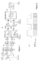
- a receiver and demodulator circuit 10 of Figure 1 comprises an antenna 20, RF amplifier 22, synchronous demodulator 30, filters 36, 37, 40, 41 and further amplifiers 38, 39, limiters 42, 43 and a four-phase detector 44.
- a transmitted FSK signal in which a data "1" state is represented by the carrier frequency modulated by, say, +f m and a data "0" state is represented by the carrier frequency modulated by -f m , is received by the antenna 20, amplified in the RF amplifier 22 and fed to the synchronous detector 30.
- the synchronous detector 30 comprises a local oscillator 32 and a 90° phase shifter 33 feeding, respectively, mixers 35 and 34.
- the RF signal from the amplifier 22 is fed to the other input of each of the mixers 34, 35 and the mixer outputs, which are in quadrature with each other, are taken to filters 36, 37, amplifiers 38, 39 and further filters 40, 41 before being amplitude-limited in limiters 42 and 43.
- the limited in-phase and quadrature signals are then processed in the four-phase detector 44, where the original transmitted data information is extracted and output along line 45.
- the filters 36, 37, 40 and 41 are all low-pass filters.
- the latter pair may, in practice, take the form of gyrators.
- An AFC circuit 50 (see Figure 3) is connected to a point B of Figure 1 and to the data output line 45.
- the baseband signal can be taken from any of points A-F, point B is chosen in this case in order to obtain a wide capture range, though this is at the expense of a narrow dynamic range, since point B is upstream of the limiting stages 42, 43.
- the baseband signal on line 51 (see Figure 3) is taken to the common pole C of a changeover switch 52, which in practice is a MOSFET analogue switch.
- the changeover poles 1, 2 of the switch 52 are connected to the inputs of frequency-to-voltage converters 54, 56, the outputs of each of which are taken to a sample-and-hold 58, 60.
- the sample-and-hold outputs feed a difference amplifier 64 which delivers, on line 66, an AFC signal for application to the oscillator 32 to be controlled.
- the data output from the FSK demodulator (line 45 of Figure 1) is taken along line 53 to the control input of the switch 52 and along line 55 to the control inputs of sample-and-holds 58, 60.
- An inverter 62 is included in the control line to one of the two sample-and-holds, so that they may be driven in anti-phase.
- the frequency of the local oscillator 32 will not remain absolutely constant, but will experience drift.
- the effect of such a drift can be seen in Figure 2, where the upper line shows the transmitted data, consisting of binary states, "1" and "0", and the lower line shows the baseband signal at any of points A-F. This baseband signal can be seen to vary in frequency, depending on the data state being transmitted.
- Converter 54 now converts the lower-than-normal baseband frequency into a corresponding voltage, which is sampled in sample-and-hold 58 and passed on to the difference amplifier 64. Meanwhile, the same change in state of the data signal has instructed the sample-and-hold 60 to hold the voltage corresponding to the higher-than-normal baseband frequency for the previous "0" data state, and this voltage is also passed on to difference amplifier 64. Difference amplifier 64 then subtracts the data "1" voltage from the data "0" voltage to form an output AFC voltage on line 66 which is fed back to the drifted oscillator 32 in such a sense as to reduce the difference between the data "1" and data "0" baseband frequencies.
- switch 52 changes over to pole 2, transferring the baseband signal on line 51 to converter 56, where its frequency is converted into a voltage which is sampled by sample-and-hold 56 and passed on to amplifier 64.
- sample-and-hold 58 is forced into its "hold” mode, so that the voltage output of converter 54 for the "1" state is held in sample-and-hold 58 and likewise fed to amplifier 64.
- Amplifier 64 forms the difference between the two voltages and sends this as a correcting signal back to the oscillator 32 as before.
- a second embodiment of the invention illustrated in Figure 4 in conjunction with Figure 1, employs digital techniques instead of analogue.
- the receiver and demodulator 10 is interfaced with a digital version 100 of the AFC circuit of the invention, the interfacing being arranged this time to allow for a wide dynamic range at the expense of capture range. This is achieved by taking the baseband signal from a point E of the receiver circuitry in Figure 1. Since this point is downstream of the limiter 42, the AFC circuit will work with an increased dynamic range over the arrangement shown in Figure 3.
- the baseband signal is taken on line 51 to the clocking inputs 75, 76 of two counters 80, 82, which correspond in this embodiment to the frequency-to-voltage converters of the previous embodiment.
- Each counter feeds a latch 84, 86, the output of which is taken to a digital subtractor 88.
- the data output signal from line 45 of Figure 1 is taken directly to gating input 83 of counter 82 and to latch-command input 85 of latch 84; similarly, an inverted version of the data output signal, by virtue of inverter 92, is taken to the gating input 81 of counter 80 and to the latch-command input 87 of latch 86.
- the output of the digital subtractor is taken to a D/A converter 90, the output of which is fed along line 94 back to the oscillator 32 whose frequency is to be corrected.
- the invention has been described in terms of the derivation of an AFC signal from a changing data output, the invention is not restricted to providing an AFC signal only when data is seen at the output. Thus, even when data is lost due to excessive drift, the arrangement according to the invention will still provide an AFC direction signal. This is primarily due to the fact that the output data signal will remain in either the high or low state when excessive frequency error occurs.
- the baseband pickup point may be at any of the points A-F, i.e. either before or after the filters 40, 41, or indeed, after the limiters 42, 43.
Landscapes
- Physics & Mathematics (AREA)
- Spectroscopy & Molecular Physics (AREA)
- Engineering & Computer Science (AREA)
- Computer Networks & Wireless Communication (AREA)
- Signal Processing (AREA)
- Digital Transmission Methods That Use Modulated Carrier Waves (AREA)
- Channel Selection Circuits, Automatic Tuning Circuits (AREA)
- Stabilization Of Oscillater, Synchronisation, Frequency Synthesizers (AREA)
- Superheterodyne Receivers (AREA)
Claims (15)
- Dispositif automatique de commande de fréquence, à utiliser dans un récepteur homodyne à manipulation par décalage de fréquence (FSK), comprenant des moyens (51, 52) d'introduction d'un signal de la bande de base venant du récepteur, et des moyens (53, 55 ; 77, 78, 92) d'introduction d'un signal de données venant du récepteur, caractérisé par des moyens (54, 56 ; 80, 82) de formation d'une première et d'une seconde valeurs représentatives de la fréquence du signal de la bande de base, pour un premier état des données et pour un second état des données, respectivement ; des moyens (58, 60, 64 ;84, 86, 88) sensibles aux moyens d'introduction (53, 55 ; 77, 78, 92) pour former la différence entre les première et seconde valeurs et établir un signal différence, et des moyens (66; 90) pour appliquer le signal différence à un oscillateur local (32) du récepteur homodyne FSK et commander la fréquence de l'oscillateur (32).
- Dispositif automatique de commande de fréquence selon la revendication 1, caractérisé en ce que les moyens de formation d'une première et d'une seconde valeurs représentatives de la fréquence du signal de la bande de base, pour un premier état des données et pour un second état des données, comprennent un premier et un second convertisseurs fréquence-tension (54, 56), respectivement, et en ce que les moyens de formation de la différence comprennent des premier et second moyens échantillonneurs-bloqueurs (58, 60) alimentés par le premier et le second moyens convertisseurs fréquence-tension (54, 56) respectivement, et un amplificateur de différence (64) ayant une première entrée alimentée par une sortie du premier moyen échantillonneur-bloqueur (58) et une seconde entrée alimentée par une sortie du second moyen échantillonneur-bloqueur (60).
- Dispositif automatique de commande de fréquence selon la revendication 2, caractérisé en ce que les moyen d'introduction d'un signal de la bande de base provenant du récepteur comprennent des moyens de commutation à bascule (52), les moyens de commutation à bascule (52) ayant une borne commune (C) qui sert à recevoir le signal de la bande de base, ainsi qu'une première et une seconde bornes de commutation (1, 2) connectées aux entrées respectives du premier et du second moyens convertisseurs fréquence-tension (54, 56).
- Dispositif automatique de commande de fréquence selon la revendication 3, caractérisé en ce que les moyens d'introduction d'un signal de données (53, 55 ; 77, 78, 92) sont disposés, lorsque le signal de données est dans son premier état, de manière à commander les moyens commutateurs à bascule (52) afin d'appliquer le signal de la bande de base au premier moyen convertisseur fréquence-tension (54), pour commander le premier moyen échantillonneur-bloqueur (58) de manière à échantillonner la première valeur, et pour commander le second moyen échantillonneur-bloqueur (60) de manière à garder la seconde valeur.
- Dispositif automatique de commande de fréquence selon la revendication 1, caractérisé en ce que les moyens de formation d'une première et d'une seconde valeurs représentatives de la fréquence du signal de base, pour un premier état des données et pour un second état des données, comprennent un moyen convertisseur fréquence-tension, et en ce que les moyens de formation de la différence comprennent un moyen commutateur à bascule, un premier et un second échantillonneurs-bloqueurs (58, 60) et un amplificateur de différence (64), dans lequel une entrée du moyen convertisseur fréquence-tension sert à recevoir le signal de la bande de base, le moyen commutateur à bascule comprend une borne commune (C), laquelle est connectée à une sortie du moyen convertisseur fréquence-tension, ainsi qu'une première et une seconde bornes de commutation (1, 2), qui sont connectées aux entrées signal respectives des premier et second moyens échantillonneurs-bloqueurs (58, 60), et l'amplificateur de différence (64) a une première entrée alimentée par la sortie du premier moyen échantillonneur-bloqueur (58) et une seconde entrée alimentée par une sortie du second moyen échantillonneur-bloqueur (60).
- Dispositif automatique de commande de fréquence selon la revendication 5, caractérisé en ce que les moyens d'introduction d'un signal de données (53, 55 ; 77, 78 ; 92) sont disposés, lorsque le signal de données est dans un premier état, de manière à commander le moyen de commutation à bascule pour connecter la sortie du moyen convertisseur fréquence-tension à l'entrée du premier moyen échantillonneur-bloqueur (58), pour commander le premier échantillonneur-bloqueur (58) de manière à échantillonner la première valeur et pour commander le second moyen échantillonneur-bloqueur (60) de manière à garder la seconde valeur.
- Dispositif automatique de commande de fréquence selon la revendication 1, caractérisé en ce que les moyens de formation d'une première et d'une seconde valeurs représentatives de la fréquence du signal de la bande de base, pour un premier état des données et pour un second état des données, comprend un premier et un second moyens de comptage (80, 82),respectivement, et en ce que le moyen de formation de la différence comprend un premier et un second moyens de loquet (84, 86) alimentés par le premier et le second moyens de comptage (80, 82), respectivement, et un moyen soustracteur numérique (88) ayant une première entrée alimentée par une sortie du premier moyen de loquet (84) et une seconde entrée alimentée par une sortie du second moyen de loquet (86).
- Dispositif automatique de commande de fréquence selon la revendication 6, caractérisé en ce que les premier et second moyens de comptage ont des entrées respectives de synchronisation (75, 76) qui sont disposées pour recevoir le signal de la bande de base, et en ce que le moyen d'introduction d'un signal de données est disposé, quand le signal de données change, de son second à son premier état de données, pour commander le premier moyen de comptage (80) de manière à démarrer le comptage, pour commander le second moyen de comptage de manière à arrêter le comptage, et pour commander le second moyen de loquet (86) de manière à verrouiller le contenu du second moyen de comptage (82), et, quand le signal de données change, de son premier à son second état, pour commander le second moyen de comptage (82) de manière à démarrer le comptage, pour commander le premier moyen de comptage (80), de manière à arrêter le comptage, et pour commander le premier moyen de loquet (84) de manière à verrouiller le contenu du premier moyen de comptage 80.
- Dispositif automatique de commande de fréquence selon la revendication 8, caractérisé en ce que la commande du premier et du second moyens de comptage (80, 82) et celle du premier et du second moyens de loquet (84, 86) se fait grâce à une première et une seconde entrées de déclenchement et à une première et une seconde entrées de commande de verrouillage respectivement appliquées aux moyens de comptage et aux moyens de verrouillage.
- Dispositif automatique de commande de fréquence selon la revendication 9, caractérisé en ce que les moyens d'application du signal différence à l'oscillateur local comprennent un convertisseur numérique-analogique (90) alimenté par la sortie du soustracteur numérique (88).
- Récepteur ou émetteur-récepteur homodyne FSK, caractérisé en ce qu'il comprend un dispositif automatique de commande de fréquence selon l'une quelconque des revendications 1 à 10.
- Procédé de commande de fréquence dans un récepteur homodyne FSK, caractérisé par les étapes consistant à: former une valeur représentative de la fréquence d'un signal de bande de base pour un premier état des données ; former une valeur représentative de la fréquence du signal de bande de base pour un second état des données ; former la différence entre les deux valeurs pour établir un signal différence, et appliquer le signal différence à un oscillateur local du récepteur pour commander la fréquence de l'oscillateur.
- Procédé de commande de fréquence dans un récepteur homodyne FSK selon la revendication 12, caractérisé par les étapes consistant à : convertir la fréquence de la bande de base, représentative d'un premier état de données en un premier signal de tension correspondant, tout en stockant un second signal de tension correspondant à la fréquence de la bande de base représentative d'un second état précédent des données convertir la fréquence de la bande de base représentative d'un second état suivant des données en un second signal de tension correspondant, tout en stockant le premier signal de tension correspondant à la fréquence de la bande de base représentative du premier état des données ; former la différence entre les deux tensions stockées et appliquer le signal différence à l'oscillateur local (32) du récepteur pour commander la fréquence de l'oscillateur (32).
- Procédé de commande de fréquence dans un récepteur homodyne FSK selon la revendication 13, caractérisé en ce que la fréquence de la bande de base est convertie en un premier et un second signaux analogiques de tension.
- Procédé de commande de fréquence dans un récepteur homodyne FSK selon la revendication 13, caractérisé en ce que la fréquence de la bande de base est convertie en premier et second signaux numériques de tension.
Applications Claiming Priority (2)
| Application Number | Priority Date | Filing Date | Title |
|---|---|---|---|
| GB9316363A GB2280801B (en) | 1993-08-06 | 1993-08-06 | Automatic frequency control arrangement |
| GB9316363 | 1993-08-06 |
Publications (2)
| Publication Number | Publication Date |
|---|---|
| EP0637882A1 EP0637882A1 (fr) | 1995-02-08 |
| EP0637882B1 true EP0637882B1 (fr) | 2001-12-19 |
Family
ID=10740097
Family Applications (1)
| Application Number | Title | Priority Date | Filing Date |
|---|---|---|---|
| EP94304951A Expired - Lifetime EP0637882B1 (fr) | 1993-08-06 | 1994-07-05 | Dispositif de commande automatique de fréquence |
Country Status (5)
| Country | Link |
|---|---|
| US (1) | US5530723A (fr) |
| EP (1) | EP0637882B1 (fr) |
| JP (1) | JP3493458B2 (fr) |
| DE (1) | DE69429476T2 (fr) |
| GB (1) | GB2280801B (fr) |
Families Citing this family (10)
| Publication number | Priority date | Publication date | Assignee | Title |
|---|---|---|---|---|
| US5701600A (en) * | 1995-07-17 | 1997-12-23 | Motorola, Inc. | Radio receiver and method of calibrating same |
| US5717721A (en) * | 1995-08-21 | 1998-02-10 | General Research Of Electronics, Inc. | Demodulation correcting circuit for FSK receiver |
| JPH10163756A (ja) * | 1996-11-28 | 1998-06-19 | Fujitsu Ltd | 自動周波数制御装置 |
| JP3070733B2 (ja) * | 1997-12-12 | 2000-07-31 | 日本電気株式会社 | 自動周波数制御方法および装置 |
| US6388248B1 (en) * | 2000-07-06 | 2002-05-14 | Eaton Corporation | Control voltage isolation system for electrical rotating apparatus utilizing fiber optics and associated method |
| KR100374944B1 (ko) * | 2001-02-02 | 2003-03-06 | 주식회사 젤라인 | 전력선통신용 주파수편이변조형 수신기의 동기장치 |
| US7369849B2 (en) * | 2002-08-06 | 2008-05-06 | General Motors Corporation | Method and system for registering an in-vehicle cellular phone |
| US7680224B2 (en) * | 2004-08-27 | 2010-03-16 | Silicon Laboratories Inc. | Apparatus and method for automatic frequency correction for a receiver system |
| US7822397B2 (en) * | 2004-08-27 | 2010-10-26 | Silicon Laboratories Inc. | Method and apparatus for frequency hopping medium access control in a wireless network |
| US7672356B2 (en) | 2005-05-19 | 2010-03-02 | Itt Manufacturing Enterprises, Inc. | Method and apparatus for detection of a frequency coded sequence in the presence of sinusoidal interference |
Family Cites Families (7)
| Publication number | Priority date | Publication date | Assignee | Title |
|---|---|---|---|---|
| GB2109201B (en) * | 1981-10-26 | 1985-03-27 | Philips Electronic Associated | Direct modulation fm receiver |
| GB2137836B (en) * | 1983-04-06 | 1986-07-23 | Multitone Electronics Plc | Fm demodulators |
| US4647864A (en) * | 1986-04-21 | 1987-03-03 | General Electric Company | Variable-delay, sine-cosine non-coherent demodulator |
| GB2213663A (en) * | 1987-12-11 | 1989-08-16 | Philips Electronic Associated | Data demodulator carrier phase locking |
| DE4013384A1 (de) * | 1990-04-26 | 1991-10-31 | Philips Patentverwaltung | Empfaenger mit einer anordnung zur frequenzablagenschaetzung |
| JPH0813049B2 (ja) * | 1990-06-20 | 1996-02-07 | 三菱電機株式会社 | 周波数誤差検出装置 |
| US5208835A (en) * | 1990-09-24 | 1993-05-04 | In-Situ, Inc. | Automatic frequency control system and method for frequency-shift-key data transmission systems |
-
1993
- 1993-08-06 GB GB9316363A patent/GB2280801B/en not_active Expired - Fee Related
-
1994
- 1994-07-05 DE DE69429476T patent/DE69429476T2/de not_active Expired - Fee Related
- 1994-07-05 EP EP94304951A patent/EP0637882B1/fr not_active Expired - Lifetime
- 1994-07-29 JP JP19623794A patent/JP3493458B2/ja not_active Expired - Fee Related
- 1994-08-03 US US08/285,407 patent/US5530723A/en not_active Expired - Lifetime
Also Published As
| Publication number | Publication date |
|---|---|
| DE69429476T2 (de) | 2002-05-16 |
| GB2280801B (en) | 1997-12-10 |
| GB9316363D0 (en) | 1993-09-29 |
| DE69429476D1 (de) | 2002-01-31 |
| JPH07170302A (ja) | 1995-07-04 |
| JP3493458B2 (ja) | 2004-02-03 |
| US5530723A (en) | 1996-06-25 |
| GB2280801A (en) | 1995-02-08 |
| EP0637882A1 (fr) | 1995-02-08 |
Similar Documents
| Publication | Publication Date | Title |
|---|---|---|
| US5584068A (en) | Direct conversion receiver | |
| WO1994016505B1 (fr) | Demodulateur par deplacement de phase | |
| CA1235754A (fr) | Demodulateur numerique de signaux en quadrature | |
| US6539066B1 (en) | Integrable radio receiver circuit for frequency-modulated digital signals | |
| US5648985A (en) | Universal radio architecture for low-tier personal communication system | |
| US5440268A (en) | AFC circuit for QPSK demodulator | |
| EP0141422B1 (fr) | Détecteur de fréquence | |
| EP0637882B1 (fr) | Dispositif de commande automatique de fréquence | |
| US3940695A (en) | Doppler correction of transmission frequencies | |
| US5539355A (en) | Frequency-shift-keying detector using digital circuits | |
| ES8402479A1 (es) | Un demodulador de banda base para senales de fm. | |
| EP0651520B1 (fr) | Dispositifs de contrôle pour des radiorécepteurs numériques | |
| EP0054323B1 (fr) | Déphaseur pour impulsions d'horloge | |
| US5926750A (en) | Receiver | |
| JPS5831065B2 (ja) | Fsk復調装置 | |
| US5307378A (en) | Digital radio communication apparatus | |
| EP0259867B1 (fr) | Démodulateur pour signaux modulés en PSK | |
| US5193103A (en) | Digital phase locked loop circuit | |
| CA2242075A1 (fr) | Demodulateur de signaux modules par deplacement de frequence a 4 niveaux | |
| CN1104820A (zh) | 检波器 | |
| US4757272A (en) | Four phase PSK demodulator | |
| US3108158A (en) | Synchronous detection multiplex system | |
| EP0151394B1 (fr) | Démodulateur pour des signaux numériques à modulation de fréquence | |
| US5020079A (en) | Apparatus for generating a minimum-shift-keying signal | |
| EP0134600B1 (fr) | Circuit démodulateur pour modulation de fréquence |
Legal Events
| Date | Code | Title | Description |
|---|---|---|---|
| PUAI | Public reference made under article 153(3) epc to a published international application that has entered the european phase |
Free format text: ORIGINAL CODE: 0009012 |
|
| AK | Designated contracting states |
Kind code of ref document: A1 Designated state(s): DE FR |
|
| 17P | Request for examination filed |
Effective date: 19950804 |
|
| RAP1 | Party data changed (applicant data changed or rights of an application transferred) |
Owner name: MITEL SEMICONDUCTOR LIMITED |
|
| 17Q | First examination report despatched |
Effective date: 20000407 |
|
| GRAG | Despatch of communication of intention to grant |
Free format text: ORIGINAL CODE: EPIDOS AGRA |
|
| GRAG | Despatch of communication of intention to grant |
Free format text: ORIGINAL CODE: EPIDOS AGRA |
|
| GRAH | Despatch of communication of intention to grant a patent |
Free format text: ORIGINAL CODE: EPIDOS IGRA |
|
| GRAH | Despatch of communication of intention to grant a patent |
Free format text: ORIGINAL CODE: EPIDOS IGRA |
|
| GRAA | (expected) grant |
Free format text: ORIGINAL CODE: 0009210 |
|
| AK | Designated contracting states |
Kind code of ref document: B1 Designated state(s): DE FR |
|
| REF | Corresponds to: |
Ref document number: 69429476 Country of ref document: DE Date of ref document: 20020131 |
|
| PLBE | No opposition filed within time limit |
Free format text: ORIGINAL CODE: 0009261 |
|
| STAA | Information on the status of an ep patent application or granted ep patent |
Free format text: STATUS: NO OPPOSITION FILED WITHIN TIME LIMIT |
|
| 26N | No opposition filed | ||
| REG | Reference to a national code |
Ref country code: FR Ref legal event code: CD |
|
| PGFP | Annual fee paid to national office [announced via postgrant information from national office to epo] |
Ref country code: FR Payment date: 20030711 Year of fee payment: 10 |
|
| PGFP | Annual fee paid to national office [announced via postgrant information from national office to epo] |
Ref country code: DE Payment date: 20030717 Year of fee payment: 10 |
|
| PG25 | Lapsed in a contracting state [announced via postgrant information from national office to epo] |
Ref country code: DE Free format text: LAPSE BECAUSE OF NON-PAYMENT OF DUE FEES Effective date: 20050201 |
|
| PG25 | Lapsed in a contracting state [announced via postgrant information from national office to epo] |
Ref country code: FR Free format text: LAPSE BECAUSE OF NON-PAYMENT OF DUE FEES Effective date: 20050331 |
|
| REG | Reference to a national code |
Ref country code: FR Ref legal event code: ST |