EP0640917A2 - Roll-Callschaltung für Halbleiterspeicher - Google Patents
Roll-Callschaltung für Halbleiterspeicher Download PDFInfo
- Publication number
- EP0640917A2 EP0640917A2 EP94113393A EP94113393A EP0640917A2 EP 0640917 A2 EP0640917 A2 EP 0640917A2 EP 94113393 A EP94113393 A EP 94113393A EP 94113393 A EP94113393 A EP 94113393A EP 0640917 A2 EP0640917 A2 EP 0640917A2
- Authority
- EP
- European Patent Office
- Prior art keywords
- roll call
- circuit
- transistors
- group
- signal
- Prior art date
- Legal status (The legal status is an assumption and is not a legal conclusion. Google has not performed a legal analysis and makes no representation as to the accuracy of the status listed.)
- Granted
Links
Images


Classifications
-
- G—PHYSICS
- G11—INFORMATION STORAGE
- G11C—STATIC STORES
- G11C29/00—Checking stores for correct operation ; Subsequent repair; Testing stores during standby or offline operation
- G11C29/70—Masking faults in memories by using spares or by reconfiguring
- G11C29/78—Masking faults in memories by using spares or by reconfiguring using programmable devices
- G11C29/835—Masking faults in memories by using spares or by reconfiguring using programmable devices with roll call arrangements for redundant substitutions
-
- G—PHYSICS
- G11—INFORMATION STORAGE
- G11C—STATIC STORES
- G11C29/00—Checking stores for correct operation ; Subsequent repair; Testing stores during standby or offline operation
- G11C29/70—Masking faults in memories by using spares or by reconfiguring
- G11C29/78—Masking faults in memories by using spares or by reconfiguring using programmable devices
- G11C29/80—Masking faults in memories by using spares or by reconfiguring using programmable devices with improved layout
- G11C29/808—Masking faults in memories by using spares or by reconfiguring using programmable devices with improved layout using a flexible replacement scheme
Definitions
- the present invention relates to a roll call circuit, and more specifically to a roll call reading circuit for a semiconductor memory having a plurality of redundant word lines or a plurality of redundant column lines.
- Recent semiconductor memories are inclined to have a large storage capacity, and therefore, have an increased number of word lines and column lines. With this inclination, the recent semiconductor memories have redundant word lines and redundant column lines for lowering a fraction defective. Therefore, most of the semiconductor memories are provided with a roll call circuit for discriminating use or non-use of each redundant memory line (such as redundant word lines and redundant column lines) at the time of evaluating a product and of analyzing a defective product.
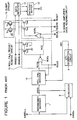
- the shown conventional roll call circuit includes a data-out buffer 12 for outputting data on an input/output pad I/O, a data amplifier 17 for amplifying data on a pair of complementary lines RWBST and RWBSN of an internal read/write bus so as to supply the amplified data to the data-out buffer 12, a sense amplifier data reading circuit 16 receiving a memory cell data from a sense amplifier (not shown in Figure 1) to supply the received memory cell data to the pair of complementary lines RWBST and RWBSN, and a roll call result reading circuit 15 for supplying a roll call discrimination result to the pair of complementary lines RWBST and RWBSN.
- the shown conventional roll call circuit includes a redundancy decoder 1 receiving internal address signals XADD1 to XADD9 which correspond to an X address supplied to external address input pins A1 to A9 (not shown), respectively. For example, if the X address supplied to the address input pin A1 is "1", the signal XADD1 is brought to a logical high level, or the X address supplied to the address input pin A1 is "0" (zero), the signal XADD1 is brought to a logical low level. Similarly, the signals XADD2 to XADD9 are brought to the logical high level or the logical low level in accordance with the value of the X address supplied to the address input pins A2 to A9, respectively.
- This redundancy decoder 1 determines whether or not a redundancy word line should be selected.
- the shown conventional roll call circuit also includes an X decoder 6 receiving the signals XADD1 to XADD9, an internal address signal XADD0 brought to the logical high level or the logical low level in accordance with the value of the X address supplied to an external address input pins A0 (not shown), and an output XRDS of the redundancy decoder 1.
- This X decoder 6 determines on the basis of its inputs XADD0, XADD1 to XADD9, which of words lines should be selected.
- the shown conventional roll call circuit furthermore includes a roll call decoder 14 receiving the output XRDS of the redundancy decoder 1, a one-shot precharge signal YRD generated by an ATD generation circuit 9, and a signal RCLB.
- the one-shot precharge signal YRD generated by the ATD generation circuit 9 is used for precharging a dynamic circuit (not shown in Figure 1) incorporated in the roll call decoder 14.
- the roll call decoder 14 At the time of a roll call testing, the roll call decoder 14 generates an output RCSB on the basis of the result of the roll call testing
- the sense amplifier data reading circuit 16 includes a pair of transfer gates composed of N-channel transistors Tr45 and Tr46, respectively, which are respectively connected between the pair of complementary lines RWBST and RWBSN and a pair of complementary data lines READT and READN from the sense amplifier, and a NOR gate NOR3 for outputting a control signal to a gate of each of the transfer gate transistors Tr45 and Tr46.
- the NOR gate NOR3 has one input connected to receive an input signal BSLB and the other input connected to receive an output RCE of the roll call result reading circuit 15.
- the roll call result reading circuit 15 includes a NOR gate NOR2 having one input connected to an output RCSB of the roll call decoder 14 and the other input connected to receive the signal RCLB, a transfer gate N-channel transistor Tr43 connected between the line RWBSN and ground and having a gate connected to an output of the NOR gate NOR2, and another transfer gate N-channel transistor Tr44 connected between a voltage supply line and the line RWBST and having a gate connected to the output of the NOR gate NOR2.
- the pair of complementary lines RWBST and RWBSN are clamped to a voltage supply voltage by means of a clamp circuit 13 formed of a pair of a gate-grounded P-channel transistors Tr9 and Tr10 connected between the voltage supply line and the pair of complementary lines RWBST and RWBSN, respectively.
- the signal RCLB is a test mode activation signal which is brought to the logical low level only when the roll call test is carries out. Therefore, at the time of reading the memory cell data, since signal RCLB is at the logical high level, the signal RCE is at the logical low level. Accordingly, during a low period of the input signal BSLB, the N-channel transistors Tr45 and Tr46 are ON, so that the sense amplifier data READT and READN are transferred to the lines RWBST and RWBSN, respectively, and therefore, amplified by the data amplifier 17 so as to outputted through the data-out buffer 12 to the input/output pad I/O. In this condition, since the signal RCE is at the logical low level, the N-channel transistors Tr43 and Tr44 are OFF, and therefore, no data is sent from the roll call result reading circuit 15 to the lines RWBST and RWBSN.
- the signal RCLB is brought to the logical low level. Therefore, the data on the lines RWBST and RWBSN.is determined by the level of the output signal RCSB of the roll call result reading circuit 14. If the output signal RCSB is at the logical low level, the signal RCE is brought to the logical high level, so that the N-channel transistors Tr43 and Tr44 are ON and the N-channel transistors Tr45 and Tr46 are OFF. Accordingly, the line RWBST is brought to the logical high level, and the line RWBSN is brought to the logical low level. This data is amplified by the data amplifier 17 and outputted through the data-out buffer 12 to the input/output pad I/O.
- the sense amplifier data is transferred to the lines RWBST and RWBSN, and amplified by the data amplifier 17 so as to outputted through the data-out buffer 12 to the input/output pad I/O.
- the roll call decoder 14 generates an output RCSB on the basis of the result of the roll call testing. Therefore, if the memory cell is previously written to the effect that the sense amplifier data READT is at the logical high level and the sense amplifier data READN is at the logical low level, the data outputted on the input/output pad I/O changes dependently upon whether the signal RSSB is at the logical high level or at the logical low level.
- the shown roll call decoder 14 includes an inverter INV14 receiving the one-shot precharge signal YRD, a P-channel transistor Tr48 having a gate connected to an output of the inverter INV14, and another P-channel transistor Tr47 having a gate connected to receive the input signal RCLB. These transistors Tr47 and Tr48 are connected in series between the voltage supply line and a precharge node "N". The input signal RCLB is also applied to a gate of an N-channel transistor Tr49, which is connected between the precharge node "N" and ground.
- N-channel transistor Tr50 which has a gate connected to receive the output signal XRDS, is also connected between the precharge node “N” and ground.
- the precharge node “N” is connected to a cascaded inverters INV15 and INV16, which operate to buffer a level on the precharge node “N” so as to generate the output RCSB.
- the precharge node "N" is precharged to the voltage supply voltage level during the logical high level period of the one-shot precharge signal YRD. If the input signal XRDS is at the high level, a level on the precharge node “N” is determined by a resistance division ratio of the transistors Tr47, Tr48 and Tr50.
- the inverter INV15 is set or configured to have such a threshold that the inverter INV16 outputs a logical high level as the output RSCB at this time.
- the input RCLB is at the logical high level, and therefore, the transistor Tr49 is ON so that the precharge node "N" is fixed to a ground level.
- the XRDS is at the logical high level, and if the redundancy word line is not used, the XRDS is at the logical low level. Therefore, the roll call can be realized.
- Another object of the present invention is to provide a roll call circuit for a semiconductor memory having a plurality of redundant word or column lines, which roll call circuit can perform the roll call test even if the semiconductor memory is a defective product having a defect in a memory cell.
- Still another object of the present invention is to provide a roll call circuit for a semiconductor memory having a plurality of redundant word or column lines, which roll call circuit can text use or non-use of the plurality of redundant word or column lines by use of one roll call decoder.
- a roll call circuit for a semiconductor memory having a plurality of redundant memory cells, the roll call circuit comprising a circuit for cutting off a path for transferring a memory cell information to an output pad at the time of a roll call test, and another circuit for transferring the result of the roll call test to the path so that the result of the roll call test is outputted from the output pad at the time of the roll call test.
- FIG 3 there is shown a circuit diagram of one embodiment of the roll call circuit in accordance with the present invention.
- elements similar or corresponding to those shown in Figure 1 are given the same Reference Numerals or Signs.
- the shown embodiment includes a data-out buffer 12 for outputting data onto an input/output pad I/O, a data amplifier 11 for amplifying data on a pair of complementary lines RWBST and RWBSN of an internal read/write bus so as to supply the amplified data to the data-out buffer 12, a sense amplifier data reading circuit 8 receiving a memory cell data from a sense amplifier 20 to supply the received memory cell data to the pair of complementary lines RWBST and RWBSN, and a roll call result reading circuit 7 for supplying a roll call discrimination result to the pair of complementary lines RWBST and RWBSN.
- the sense amplifier 20 is coupled to a memory cell matrix including a number of memory cells 22 and a plurality of redundant memory cells 24, which are arranged in the form of a matrix having a plurality of rows and a plurality of columns.
- the shown embodiment includes four redundancy decoders 1, 2, 3 and 4 each receiving internal address signals XADD1 to XADD9 for determining whether or not a redundancy word line should be selected, an X decoder 6 receiving the signals XADD1 to XADD9, another internal address signal XADD0 and redundancy selection signals XRDS1, XRDS2, XRDS3 and XRDS4 outputted from the redundancy decoders 1, 2, 3 and 4, for the purpose of determining which of words lines should be selected.
- the shown embodiment also includes a roll call decoder 5 receiving the redundancy selection signals XRDS1, XRDS2, XRDS3 and XRDS4 of the redundancy decoders 1, 2, 3 and 4, the signal XADD0, an internal address signal YADD0, a one-shot precharge signal YRD generated by an ATD generation circuit 9, and a signal RCLB.
- the internal address signal YADD0 is brought to the logical high level when "1" is given as a Y address or the logical low level when "0" is given as a Y address.
- the one-shot precharge signal YRD generated by the ATD generation circuit 9 is used for precharging a dynamic circuit (not shown in Figure 3) incorporated in the roll call decoder 5.
- the roll call decoder 5 At the time of a roll call testing, the roll call decoder 5 generates an output RCSB on the basis of the result of the roll call testing.
- the sense amplifier data reading circuit 8 includes a data amplifier 10 having a pair of complementary inputs connected to a pair of complementary data output lines READT and READN of the sense amplifier 20, respectively.
- a pair of complementary data outputs of the data amplifier 10 are connected to a gate of two source-grounded N-channel transistors Tr6 and Tr8, respectively.
- a transfer gate N-channel transistor Tr5 is connected between the line RWBSN and a drain of the transistor Tr6, and an another transfer gate N-channel transistor Tr7 is connected between the line RWBST and a drain of the transistor Tr8.
- the sense amplifier data reading circuit 8 also includes an NAND gate NAND2 receiving the signal YRD and the signal RCLB, and a NOR gate NOR1 receiving an output DEDB of the NAND gate NAND2 and a signal BSLB and having an output connected to a gate of each of the transfer gate transistors Tr5 and Tr7.
- the roll call result reading circuit 7 includes an N-channel transistor Tr4 having a drain connected to a high voltage supply voltage and a gate connected to an output RCSB of the roll call decoder 5, an inverter INV3 receiving the output RCSB of the roll call decoder 5, a source-grounded N-channel transistor Tr2 having a gate connected to an output of the inverter INV3, a transfer gate N-channel transistor Tr1 connected between the line RWBSN and a drain of the transistor Tr2, and an another transfer gate N-channel transistor Tr3 connected between the line RWBST and a source of the transistor Tr4.
- the roll call result reading circuit 7 further includes an inverter INV1 receiving the signal RCLB, a NAND gate NAND1 receiving an output of the inverter INV1 and the signal YRD, and another inverter INV2 having an input connected to an output of the NAND gate NAND1 and also having an output DEDR connected to a gate of each of the transfer gate N-channel transistor Tr1 and Tr3.
- the pair of complementary lines RWBST and RWBSN are clamped to the high voltage supply voltage by means of a clamp circuit 13 formed of a pair of a gate-grounded P-channel transistors Tr9 and Tr10 connected between the high voltage supply voltage and the pair of complementary lines RWBST and RWBSN, respectively.
- the signal DEDB is brought to the logical low level during a high level period of the one-shot precharge signal YRD. Accordingly, when the input signal BSLB is at the logical low level, the transfer gate N-channel transistors Tr5 and Tr7 are turned ON, so that a voltage difference is created between the lines RWBST and RWBSN, as the result of an amplification function of the data amplifier 10 which amplifies the memory cell data from the sense amplifier 20. At this time, since the signal DEDR is at the logical low level, the transfer gate N-channel transistors Tr1 and Tr3 are OFF, and therefore, no data is transferred from the roll call result reading circuit 7 to the lines RWBST and RWBSN.
- the signal DEDR is brought to the logical high level during a period in which the one-shot precharge signal YRD is at a logical high level, so that the transfer gate N-channel transistors Tr1 and Tr3 are turned ON. Accordingly, a voltage difference is created between the lines RWBST and RWBSN in accordance with the condition of the output RCSB of the roll call decoder 5. On the other hand, since the transfer gate N-channel transistors Tr5 and Tr7 are OFF, the lines RWBST and RWBSN are isolated from the data amplifier 10.
- FIG. 4 there is shown a circuit diagram of one example of the roll call decoder 5 included in the roll call circuit shown in Figure 3.
- the roll call decoder 5 includes an inverter INV4 receiving the one-shot precharge signal YRD, a P-channel transistor Tr24 having a gate connected to an output of the inverter INV4, and another P-channel transistor Tr23 having a gate connected to receive the input signal RCLB. These transistors Tr23 and Tr24 are connected in series between the high voltage supply voltage and a precharge node "N". The input signal RCLB is also applied to a gate of an N-channel transistor Tr25, which is connected between the precharge node "N" and ground.
- each of which is composed of three series-connected N-channel transistors Tr11, Tr12 and Tr13, Tr14, Tr15 and Tr16, Tr17, Tr18 and Tr19, or Tr20, Tr21 and Tr22.
- a gate of the transistors Tr11, Tr14, Tr17 and Tr20 are connected to receive the signals XRDS1, XRDS2, XRDS3 and XRDS4, respectively.
- a gate of the transistors Tr12 and Tr18 are connected to receive the signal XADD0, and a gate of the transistors Tr15 and Tr21 are connected to an output of an inverter INV5 having an input receiving the signal XADD0.
- a gate of the transistors Tr13 and Tr16 are connected to receive the signal YADD0, and a gate of the transistors Tr19 and Tr22 are connected to an output of an inverter INV6 having an input receiving the signal YADD0.
- the precharge node “N” is connected to an input of an inverter INV7, which has an output connected to an input of an inverter INV8, which generates the signal RCSB at its output.
- the precharge node "N" is precharged to the high voltage supply voltage level during the logical high level period of the one-shot precharge signal YRD.
- the inverter INV7 is set or configured to have such a threshold that the inverter INV8 outputs a logical high level as the output RSCB at this time.
- the four redundancy selection signals XRDS1, XRDS2, XRDS3 and XRDS4 are supplied to the roll call decoder 5.
- Each of these redundancy selection signals XRDS1, XRDS2, XRDS3 and XRDS4 selects a redundant word line independent of each other. If the redundant word line is used, a corresponding redundancy selection signal XRDS1, XRDS2, XRDS3 or XRDS4 is at the logical high level. Otherwise, the redundancy selection signal XRDS1, XRDS2, XRDS3 or XRDS4 is at the logical low level.
- the level of the redundancy selection signals XRDS2, XRDS3 and XRDS4 can be known by controlling XADD0 and YADD0.
- redundancy selection signals XRDS1, XRDS2, XRDS3 and XRDS4 are at the logical high level or at the logical low level, is determined by a combination of XADD1 to XADD9.
- the use or non-use of the redundant word lines is determined independently of XADD0 and the Y address.
- the input RCLB is at the logical high level, and therefore, the transistor Tr25 is ON so that the precharge node "N" is fixed to a ground level.
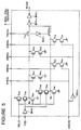
- FIG. 5 there is shown a circuit diagram of another example of the roll call decoder 5 included in the roll call circuit shown in Figure 3.
- the second embodiment of the roll call decoder 5 includes an inverter INV9 receiving the one-shot precharge signal YRD, a P-channel transistor Tr36 having a gate connected to an output of the inverter INV9, and another P-channel transistor Tr35 having a gate connected to receive the input signal RCLB. These transistors Tr35 and Tr36 are connected in series between the high voltage supply voltage and a first precharge node "N1".
- the input signal RCLB is also applied to a gate of an N-channel transistor Tr37, which is connected between the first precharge node "N1" and ground.
- the second embodiment of the roll call decoder 5 also includes a P-channel transistor Tr39 having a gate connected to an output of the inverter INV9, and another P-channel transistor Tr38 having a gate connected to receive the input signal RCLB. These transistors Tr38 and Tr39 are connected in series between the high voltage supply voltage and a second precharge node "N2".
- the input signal RCLB is also applied to a gate of an N-channel transistor Tr40, which is connected between the second precharge node "N2" and ground.
- a gate of the transistors Tr27, Tr31, Tr29 and Tr33 are connected to receive the signals XRDS1, XRDS2, XRDS3 and XRDS4, respectively.
- a gate of the transistors Tr28 and Tr32 are connected to receive the signal XADD0, and a gate of the transistors Tr30 and Tr34 are connected to an output of an inverter INV10 having an input receiving the signal XADD0.
- the first precharge node “N1" is connected through a transfer gate N-channel transistor Tr41 to an input of an inverter INV12
- the second precharge node “N2” is connected through a transfer gate N-channel transistor Tr42 to the input of the inverter INV12.
- An output of the inverter INV12 is connected to an input of another inverter INV13, which outputs the signal RCSB.
- a gate of the transistor Tr41 is connected to receive the signal YADD0
- a gate of the transistor Tr42 is connected to an output of an inverter INV11 having an input receiving the signal YADD0.
- the level of the first and second precharge nodes "N1" and “N2” are determined in accordance with the redundancy selection signals XRDS1, XRDS2 XRDS3 and XRDS4 and XADD0, and one of the first and second precharge nodes "N1" and “N2" is supplied to the inverter INV12 through the transfer gates controlled by YADD0.
- the level of the first and second precharge nodes "N1" and "N2" is determined by the resistance division ratio of the four transistors. Namely, since the number of the series-connected transistors is reduced, the ON resistance of the transistors becomes small.
- XADD0 and YADD0 are used for selecting the redundancy selection signals XRDS1, XRDS2, XRDS3 and XRDS4.
- XRDS1, XRDS2, XRDS3 and XRDS4 are used for selecting the redundancy selection signals XRDS1, XRDS2, XRDS3 and XRDS4.
- the roll call circuit in accordance with the present invention is constructed to output the roll call result without reading out the memory cell information, it is possible to carry out the roll call testing even if the semiconductor memory is a defective product having a defect in a memory cell.
- the roll call circuit in accordance with the present invention is so constructed that a plurality of redundancy selection signals are supplied to one roll call decoder and decoded or selected by utilizing address bits which are influenced by the selection and non-selection of the redundant word or column lines, it is possible text use or non-use of the plurality of redundant word or column lines by use of the one roll call decoder. Therefore, it is possible to reduce the required circuit area and the required number of external pads.
Landscapes
- For Increasing The Reliability Of Semiconductor Memories (AREA)
- Static Random-Access Memory (AREA)
- Dram (AREA)
- Read Only Memory (AREA)
Applications Claiming Priority (3)
| Application Number | Priority Date | Filing Date | Title |
|---|---|---|---|
| JP21131993 | 1993-08-26 | ||
| JP211319/93 | 1993-08-26 | ||
| JP21131993A JP2570589B2 (ja) | 1993-08-26 | 1993-08-26 | ロールコール回路 |
Publications (3)
| Publication Number | Publication Date |
|---|---|
| EP0640917A2 true EP0640917A2 (de) | 1995-03-01 |
| EP0640917A3 EP0640917A3 (de) | 1998-03-18 |
| EP0640917B1 EP0640917B1 (de) | 2003-05-21 |
Family
ID=16603983
Family Applications (1)
| Application Number | Title | Priority Date | Filing Date |
|---|---|---|---|
| EP94113393A Expired - Lifetime EP0640917B1 (de) | 1993-08-26 | 1994-08-26 | Roll-Callschaltung für Halbleiterspeicher |
Country Status (5)
| Country | Link |
|---|---|
| US (1) | US5517458A (de) |
| EP (1) | EP0640917B1 (de) |
| JP (1) | JP2570589B2 (de) |
| KR (1) | KR0138716B1 (de) |
| DE (1) | DE69432690T2 (de) |
Cited By (1)
| Publication number | Priority date | Publication date | Assignee | Title |
|---|---|---|---|---|
| EP1115063A1 (de) * | 2000-01-06 | 2001-07-11 | Fujitsu Limited | Nichtflüchtige Halbleiterspeicheranordnung mit Fehlersteuerung |
Families Citing this family (6)
| Publication number | Priority date | Publication date | Assignee | Title |
|---|---|---|---|---|
| JP2848339B2 (ja) * | 1996-06-14 | 1999-01-20 | 日本電気株式会社 | 冗長デコード回路 |
| JP2930029B2 (ja) * | 1996-09-20 | 1999-08-03 | 日本電気株式会社 | 半導体メモリ装置 |
| JP3168985B2 (ja) * | 1998-06-04 | 2001-05-21 | 日本電気株式会社 | ロールコールテスト装置 |
| JP3339446B2 (ja) * | 1999-02-09 | 2002-10-28 | 日本電気株式会社 | 半導体記憶装置 |
| JP2014186785A (ja) * | 2013-03-25 | 2014-10-02 | Micron Technology Inc | 半導体装置 |
| JP7171286B2 (ja) * | 2018-07-20 | 2022-11-15 | ラピスセミコンダクタ株式会社 | 半導体メモリ装置 |
Family Cites Families (7)
| Publication number | Priority date | Publication date | Assignee | Title |
|---|---|---|---|---|
| DE3311427A1 (de) * | 1983-03-29 | 1984-10-04 | Siemens AG, 1000 Berlin und 8000 München | Integrierter dynamischer schreib-lesespeicher |
| EP0241203A3 (de) * | 1986-04-03 | 1989-08-09 | Advanced Micro Devices, Inc. | Erkennung von reparierten Speichergeräten |
| JPH01245497A (ja) * | 1988-03-28 | 1989-09-29 | Nec Corp | 半導体メモリ |
| JPH0322298A (ja) * | 1989-06-19 | 1991-01-30 | Nec Corp | 半導体記憶装置 |
| JPH03160695A (ja) * | 1989-11-17 | 1991-07-10 | Nec Corp | 半導体記憶装置 |
| JPH03283197A (ja) * | 1990-03-30 | 1991-12-13 | Nec Corp | 半導体メモリ |
| US5343429A (en) * | 1991-12-06 | 1994-08-30 | Mitsubishi Denki Kabushiki Kaisha | Semiconductor memory device having redundant circuit and method of testing to see whether or not redundant circuit is used therein |
-
1993
- 1993-08-26 JP JP21131993A patent/JP2570589B2/ja not_active Expired - Lifetime
-
1994
- 1994-08-25 KR KR1019940020990A patent/KR0138716B1/ko not_active Expired - Fee Related
- 1994-08-26 DE DE69432690T patent/DE69432690T2/de not_active Expired - Lifetime
- 1994-08-26 EP EP94113393A patent/EP0640917B1/de not_active Expired - Lifetime
- 1994-08-26 US US08/296,468 patent/US5517458A/en not_active Expired - Lifetime
Cited By (2)
| Publication number | Priority date | Publication date | Assignee | Title |
|---|---|---|---|---|
| EP1115063A1 (de) * | 2000-01-06 | 2001-07-11 | Fujitsu Limited | Nichtflüchtige Halbleiterspeicheranordnung mit Fehlersteuerung |
| US6288940B1 (en) | 2000-01-06 | 2001-09-11 | Fujitsu Limited | Non-volatile semiconductor memory device |
Also Published As
| Publication number | Publication date |
|---|---|
| KR0138716B1 (ko) | 1998-06-15 |
| EP0640917B1 (de) | 2003-05-21 |
| US5517458A (en) | 1996-05-14 |
| KR950006876A (ko) | 1995-03-21 |
| DE69432690T2 (de) | 2004-04-08 |
| EP0640917A3 (de) | 1998-03-18 |
| DE69432690D1 (de) | 2003-06-26 |
| JPH0765595A (ja) | 1995-03-10 |
| JP2570589B2 (ja) | 1997-01-08 |
Similar Documents
| Publication | Publication Date | Title |
|---|---|---|
| US6519192B2 (en) | Semiconductor memory device having a large band width and allowing efficient execution of redundant repair | |
| US6269035B1 (en) | Circuit and method for a multiplexed redundancy scheme in a memory device | |
| JP3691608B2 (ja) | 半導体メモリ装置 | |
| EP0335125B1 (de) | Dynamischer RAM-Speicher mit Redundanz und verbesserter Prüfbarkeit | |
| US4914632A (en) | Semiconductor devices having redundancy circuitry and operating method therefor | |
| KR100284716B1 (ko) | 반도체 기억 장치 | |
| JP2785717B2 (ja) | 半導体記憶装置 | |
| KR100252053B1 (ko) | 칼럼 방향의 데이터 입출력선을 가지는 반도체메모리장치와불량셀 구제회로 및 방법 | |
| KR937000951A (ko) | 병렬 테스트 장치를 갖는 집적 반도체 메모리와 중복방법 | |
| EP0622803B1 (de) | Adressenpuffer | |
| JPH0877776A (ja) | 半導体記憶装置 | |
| US6868021B2 (en) | Rapidly testable semiconductor memory device | |
| US6552939B1 (en) | Semiconductor memory device having disturb test circuit | |
| US6956780B2 (en) | Semiconductor memory device having direct sense amplifier implemented in hierarchical input/output line architecture | |
| EP0640917B1 (de) | Roll-Callschaltung für Halbleiterspeicher | |
| US6269033B1 (en) | Semiconductor memory device having redundancy unit for data line compensation | |
| EP0953912B1 (de) | Halbleiterspeicheranordnung mit Redundanz | |
| US6930934B2 (en) | High efficiency redundancy architecture in SRAM compiler | |
| KR20030043668A (ko) | 반도체 기억 장치 | |
| US20010053086A1 (en) | Semiconductor memory device with memory test circuit | |
| US5894440A (en) | Semiconductor memory device and data transferring structure and method therein | |
| JPH1173792A (ja) | 半導体記憶装置 | |
| US6519193B2 (en) | Semiconductor integrated circuit device having spare word lines | |
| KR0132400B1 (ko) | 반도체 메모리장치의 멀티비트 테스트회로 | |
| US6975548B2 (en) | Memory device having redundant memory cell |
Legal Events
| Date | Code | Title | Description |
|---|---|---|---|
| PUAI | Public reference made under article 153(3) epc to a published international application that has entered the european phase |
Free format text: ORIGINAL CODE: 0009012 |
|
| AK | Designated contracting states |
Kind code of ref document: A2 Designated state(s): DE FR GB NL |
|
| PUAL | Search report despatched |
Free format text: ORIGINAL CODE: 0009013 |
|
| AK | Designated contracting states |
Kind code of ref document: A3 Designated state(s): DE FR GB NL |
|
| 17P | Request for examination filed |
Effective date: 19980206 |
|
| 17Q | First examination report despatched |
Effective date: 20010906 |
|
| GRAG | Despatch of communication of intention to grant |
Free format text: ORIGINAL CODE: EPIDOS AGRA |
|
| GRAG | Despatch of communication of intention to grant |
Free format text: ORIGINAL CODE: EPIDOS AGRA |
|
| GRAH | Despatch of communication of intention to grant a patent |
Free format text: ORIGINAL CODE: EPIDOS IGRA |
|
| GRAH | Despatch of communication of intention to grant a patent |
Free format text: ORIGINAL CODE: EPIDOS IGRA |
|
| GRAA | (expected) grant |
Free format text: ORIGINAL CODE: 0009210 |
|
| RAP1 | Party data changed (applicant data changed or rights of an application transferred) |
Owner name: NEC ELECTRONICS CORPORATION Owner name: NEC CORPORATION |
|
| AK | Designated contracting states |
Designated state(s): DE FR GB NL |
|
| REG | Reference to a national code |
Ref country code: GB Ref legal event code: FG4D |
|
| REF | Corresponds to: |
Ref document number: 69432690 Country of ref document: DE Date of ref document: 20030626 Kind code of ref document: P |
|
| ET | Fr: translation filed | ||
| PLBE | No opposition filed within time limit |
Free format text: ORIGINAL CODE: 0009261 |
|
| STAA | Information on the status of an ep patent application or granted ep patent |
Free format text: STATUS: NO OPPOSITION FILED WITHIN TIME LIMIT |
|
| 26N | No opposition filed |
Effective date: 20040224 |
|
| REG | Reference to a national code |
Ref country code: GB Ref legal event code: 732E |
|
| REG | Reference to a national code |
Ref country code: FR Ref legal event code: TP |
|
| NLS | Nl: assignments of ep-patents |
Owner name: NEC ELECTRONICS CORPORATION Effective date: 20071024 |
|
| PGFP | Annual fee paid to national office [announced via postgrant information from national office to epo] |
Ref country code: FR Payment date: 20090814 Year of fee payment: 16 |
|
| PGFP | Annual fee paid to national office [announced via postgrant information from national office to epo] |
Ref country code: NL Payment date: 20090816 Year of fee payment: 16 Ref country code: GB Payment date: 20090826 Year of fee payment: 16 Ref country code: DE Payment date: 20090821 Year of fee payment: 16 |
|
| REG | Reference to a national code |
Ref country code: NL Ref legal event code: V1 Effective date: 20110301 |
|
| GBPC | Gb: european patent ceased through non-payment of renewal fee |
Effective date: 20100826 |
|
| REG | Reference to a national code |
Ref country code: FR Ref legal event code: ST Effective date: 20110502 |
|
| PG25 | Lapsed in a contracting state [announced via postgrant information from national office to epo] |
Ref country code: NL Free format text: LAPSE BECAUSE OF NON-PAYMENT OF DUE FEES Effective date: 20110301 |
|
| REG | Reference to a national code |
Ref country code: DE Ref legal event code: R119 Ref document number: 69432690 Country of ref document: DE Effective date: 20110301 |
|
| PG25 | Lapsed in a contracting state [announced via postgrant information from national office to epo] |
Ref country code: DE Free format text: LAPSE BECAUSE OF NON-PAYMENT OF DUE FEES Effective date: 20110301 Ref country code: FR Free format text: LAPSE BECAUSE OF NON-PAYMENT OF DUE FEES Effective date: 20100831 |
|
| PG25 | Lapsed in a contracting state [announced via postgrant information from national office to epo] |
Ref country code: GB Free format text: LAPSE BECAUSE OF NON-PAYMENT OF DUE FEES Effective date: 20100826 |