EP0640926A1 - Prioritätskodierer - Google Patents
Prioritätskodierer Download PDFInfo
- Publication number
- EP0640926A1 EP0640926A1 EP94410068A EP94410068A EP0640926A1 EP 0640926 A1 EP0640926 A1 EP 0640926A1 EP 94410068 A EP94410068 A EP 94410068A EP 94410068 A EP94410068 A EP 94410068A EP 0640926 A1 EP0640926 A1 EP 0640926A1
- Authority
- EP
- European Patent Office
- Prior art keywords
- request
- mask
- requests
- rank
- bits
- Prior art date
- Legal status (The legal status is an assumption and is not a legal conclusion. Google has not performed a legal analysis and makes no representation as to the accuracy of the status listed.)
- Granted
Links
Images

Classifications
-
- G—PHYSICS
- G06—COMPUTING OR CALCULATING; COUNTING
- G06F—ELECTRIC DIGITAL DATA PROCESSING
- G06F13/00—Interconnection of, or transfer of information or other signals between, memories, input/output devices or central processing units
- G06F13/14—Handling requests for interconnection or transfer
- G06F13/36—Handling requests for interconnection or transfer for access to common bus or bus system
- G06F13/362—Handling requests for interconnection or transfer for access to common bus or bus system with centralised access control
- G06F13/364—Handling requests for interconnection or transfer for access to common bus or bus system with centralised access control using independent requests or grants, e.g. using separated request and grant lines
-
- G—PHYSICS
- G06—COMPUTING OR CALCULATING; COUNTING
- G06F—ELECTRIC DIGITAL DATA PROCESSING
- G06F13/00—Interconnection of, or transfer of information or other signals between, memories, input/output devices or central processing units
- G06F13/14—Handling requests for interconnection or transfer
- G06F13/20—Handling requests for interconnection or transfer for access to input/output bus
- G06F13/24—Handling requests for interconnection or transfer for access to input/output bus using interrupt
- G06F13/26—Handling requests for interconnection or transfer for access to input/output bus using interrupt with priority control
Definitions
- the present invention relates to a priority level coder which is a circuit serving to acknowledge the highest priority request among a set of requests arriving in the form of active signals at the coder. Acknowledging a request consists in validating a circuit (often a microprocessor) so that the latter performs the task corresponding to the request.
- a priority level coder receives one or more simultaneous requests on a set of assigned request lines of respective ranks, for example from 1 to n, and acknowledges only one request at a time by acknowledgment lines.
- the acknowledgment lines correspond directly to the request lines and the encoder transmits on the acknowledgment lines only the only acknowledged request.
- the acknowledgment lines provide, in binary form, the rank of the acknowledged request.
- the priorities assigned to the request lines are distinct, the priorities being for example assigned in decreasing order to the ranks of the request lines.
- the linear coder always acknowledges the request for the lowest rank, and a request for a given rank is not acknowledged as long as there are requests for lower rank.
- a linear encoder is conventionally made up of a non-sequential logic circuit, of the carry propagation type, which acknowledges the request for the lowest rank shortly (depending on the carry propagation delay) after any change in the states query lines.
- the request lines are assigned the same priority level.
- Such an encoder must guarantee, if several requests are active at the same time, that each of these requests is acknowledged at a given time.
- a conventional circular encoder consists of a sequential logic circuit which performs a circular scanning of the request lines at the rate of a clock. At each clock cycle, the sequential circuit scans a request line. If the scanned request line is active, the corresponding acknowledgment is sent, and the scanning of the request lines continues from the last scanned line. When the request row of last rank, n, is scanned, the scanning starts again on the request row of rank 1 ...
- a disadvantage of the above-mentioned circular encoder is that it only processes one request line per clock cycle. In other words, if the circuit has just scanned the row of rank i and the next active request is of rank j (j> i), the request of rank j is only acknowledged after j-i clock cycles afterwards.
- An object of the present invention is to provide a circular priority level encoder enabling requests of any rank to be acknowledged at successive clock cycles.
- Another object of the present invention is to provide an encoder of mixed priority level making it possible, in a programmable manner, to treat part of the requests as requests of distinct priorities (linear coding) and another part of the requests as requests. of identical priority (circular coding), and this while acknowledging a request at each clock cycle.
- the masking register comprises an initialization input activated when the acknowledgment output of the linear encoder is at zero.
- the invention also provides a mixed priority level encoder further comprising means for forcing an active state of the selected bits of the masks supplied by the mask generator.
- the coder comprises means for authorizing the loading of a mask into the masking register only if the acknowledged request corresponds to the bits not forced to an active state of the masks.
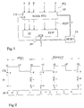
- a circular priority level coder comprises a linear priority level coder (LINP) 10.
- This linear coder receives request lines from ranks 1 to n via a register masking (MASK REG) 12.
- RQ register masking
- RQM register masking
- the acknowledgment output ACK of the linear encoder 10 is connected to a mask generator (MGEN) 14 which supplies a mask M to the masking register 12, which is a function of the rank of the request acknowledged by the linear encoder 10.
- a mask M supplied by the generator 14 comprises a bit associated with each request line RQ.
- the masking register 12 is such that an active state of a request line RQ is transmitted to the linear encoder 10 only if the corresponding bit of the mask is active, for example at 1.
- the masking register 12 receives a clock signal CK which causes, on each rising edge for example, the storage of the states of the request lines RQ and of the mask M supplied by the mask generator 14.
- the masking register includes an entry for "asynchronous S" (ie which, as soon as it is activated, sets the mask contained in the masking register to 1).
- This setting input to 1 is validated when the linear encoder 10 has no request to be acknowledged, that is to say when its ACK output is at 0.
- the ACK output is supplied to a NOR gate 16 the output of which is supplied to the input to 1S of the masking register 12.
- the mask generator 14 is such that it provides a mask whose bits of ranks 1 to i are at 0 and the remaining bits at 1 when the linear coder 10 acknowledges the request of rank i.
- Such a mask generator can be easily produced by a person skilled in the art using logic gates.
- FIG. 2 illustrates, using a timing diagram, the operation of the circular encoder according to the invention.
- This figure represents the shape of the clock signal CK, the masks M loaded in the masking register 12 and the acknowledgment ACK of various requests.
- Instants t1 to t4 designate successive rising edges of the clock CK and instants t1 'to t3' designate the falling edges.
- an initial mask is loaded into the masking register 12, all the bits of which are at 1, and the states of the request lines RQ are stored in this register.
- the linear encoder 10 does not acknowledge any request, its ACK output is at 0. All the requests on the lines RQ are transmitted to the linear encoder 10. It is assumed that only the row of rank i is active. Some time after the instant t1, for example in the vicinity of the instant t1 'at the falling edge of the clock CK, the linear coder 10 acknowledges the request i. As soon as this acknowledgment is made, the mask generator 14 establishes a mask M whose bits of ranks 1 to i are at 0 and the other bits at 1.
- the aforementioned mask established by the mask generator 14 is loaded into the masking register 12 and the states of the request lines RQ are stored.
- the lines RQ present new requests of ranks j and k (j ⁇ k) lower than rank i.
- these requests of rank j and k are masked; the linear encoder 10 receives no request.
- the linear encoder 10 supplies the value 0 on its acknowledgment output ACK.
- the masking register is set to 1 by gate 16, this which then causes the transmission of requests of rank j and k to the linear encoder 10.
- the linear encoder 10 acknowledges the request of rank j, rank j being less than rank k.
- the mask generator 14 then establishes a mask M whose bits of rank 1 to j are at 0 and the other bits at 1.
- this new mask is loaded into the masking register 12 and the new requests on the lines RQ are stored.
- the requests of rank j and k are always active. However, the request for rank j is now masked and does not reach the linear encoder 10. Only the request for rank k is transmitted to the encoder 10 which acknowledges this request in the vicinity of an instant t3 '. Upon this acknowledgment, the mask generator 14 establishes a new mask M, the bits of rank 1 to k are at 0 and the other bits to 1 ...
- the timing diagram of FIG. 2 shows that the circuit of FIG. 1 operates as a circular priority level coder which has the advantage of fulfilling an active request at each clock cycle.
- FIG. 3 shows an embodiment of a mixed priority level coder according to the present invention.
- This encoder is used to process low ranking requests as as separate priority requests (linear coding), and high ranking requests as identical priority requests (circular coding).
- linear coding linear coding
- high ranking requests identical priority requests
- a set of OR gates 18 has been added, each receiving a bit of a register (REG) 20 and a bit of a mask M1 supplied by the mask generator 14.
- the outputs of the gates OR 18 provide the mask M to the masking register 12.
- register 20 is write-accessible by the microprocessor, which makes it possible to write values to this register by program.
- the requests of rank 1 to i of the register 20 are always transmitted to the linear encoder 10.
- the requests of rank 1 to i are permanently processed so classical linear by the linear encoder 10, as requests for distinct priorities.
- the mask generator 14 operating as previously described, the remaining requests, of rows i + l to n, are processed in a circular manner.
- the linear coder 10 acknowledges the highest priority among these active requests.
- the mask generator 14 supplies each of these acknowledgments with a mask whose first bits are at 0 but which are forced to 1 by the OR gates 18.
- the circuit behaves like the circuit of FIG. 1, that is to say in a circular manner, for requests of rank higher than i.
- FIG. 4 represents an example of a logic circuit added to the circuit of FIG. 3, which allows the mixed coder according to the invention to process the requests in a circular or linear manner according to any combinations determined by the register 20.
- Each ACK acknowledgment line is connected to a first input of a respective AND gate 40.
- Each L / C line of output from register 20 is connected to a second, inverting input of the corresponding AND gate 40.
- the outputs of the doors 40 are connected to an OR gate 42.
- the output of gate 42 is active only when a circular priority request is acknowledged.
- the output of this gate 42 validates the transmission of the clock signal CK to the masking register 12 by means of an AND gate 44. Consequently, a new mask M is loaded into the masking register 12 only if a request for circular priority is acknowledged.
Landscapes
- Engineering & Computer Science (AREA)
- Theoretical Computer Science (AREA)
- Physics & Mathematics (AREA)
- General Engineering & Computer Science (AREA)
- General Physics & Mathematics (AREA)
- Communication Control (AREA)
- Electronic Switches (AREA)
Applications Claiming Priority (2)
| Application Number | Priority Date | Filing Date | Title |
|---|---|---|---|
| FR9310576 | 1993-08-31 | ||
| FR9310576A FR2709579B1 (fr) | 1993-08-31 | 1993-08-31 | Codeur de niveau de priorité. |
Publications (2)
| Publication Number | Publication Date |
|---|---|
| EP0640926A1 true EP0640926A1 (de) | 1995-03-01 |
| EP0640926B1 EP0640926B1 (de) | 2001-11-07 |
Family
ID=9450587
Family Applications (1)
| Application Number | Title | Priority Date | Filing Date |
|---|---|---|---|
| EP94410068A Expired - Lifetime EP0640926B1 (de) | 1993-08-31 | 1994-08-29 | Prioritätskodierer |
Country Status (5)
| Country | Link |
|---|---|
| US (1) | US5568485A (de) |
| EP (1) | EP0640926B1 (de) |
| JP (1) | JPH07152586A (de) |
| DE (1) | DE69428953T2 (de) |
| FR (1) | FR2709579B1 (de) |
Cited By (1)
| Publication number | Priority date | Publication date | Assignee | Title |
|---|---|---|---|---|
| EP0782081A1 (de) * | 1995-12-29 | 1997-07-02 | BULL HN INFORMATION SYSTEMS ITALIA S.p.A. | Arbitrierungseinheit mit kreisförmiger Priorität, insbesondere für Multiprozessorsysteme mit synchronen symmetrischen Prozessoren |
Families Citing this family (12)
| Publication number | Priority date | Publication date | Assignee | Title |
|---|---|---|---|---|
| DE69426625T2 (de) * | 1994-09-28 | 2001-09-06 | Stmicroelectronics S.R.L., Agrate Brianza | Steuerungseinheit für Unterbrechungskanäle in einem Mikrokontroller |
| US6681315B1 (en) | 1997-11-26 | 2004-01-20 | International Business Machines Corporation | Method and apparatus for bit vector array |
| US6028452A (en) * | 1998-02-27 | 2000-02-22 | Digital Equipment Corporation | Method and apparatus for a fast variable precedence priority encoder with optimized round robin precedence update scheme |
| AU745572B2 (en) * | 1998-11-16 | 2002-03-21 | Canon Kabushiki Kaisha | Multi-Level random access priority encoder |
| US6591331B1 (en) | 1999-12-06 | 2003-07-08 | Netlogic Microsystems, Inc. | Method and apparatus for determining the address of the highest priority matching entry in a segmented content addressable memory device |
| US6647449B1 (en) * | 2000-10-05 | 2003-11-11 | Hewlett-Packard Development Company, L.P. | System, method and circuit for performing round robin arbitration |
| US6696988B2 (en) | 2000-12-29 | 2004-02-24 | Intel Corporation | Method and apparatus for implementing circular priority encoder |
| US6868529B1 (en) * | 2001-08-31 | 2005-03-15 | Turin Networks | Method and apparatus for efficient implementation of round robin control unit |
| US7099972B2 (en) * | 2002-07-03 | 2006-08-29 | Sun Microsystems, Inc. | Preemptive round robin arbiter |
| US7236499B2 (en) * | 2003-06-23 | 2007-06-26 | Intel Corporation | Resource arbitration in accordance with a masked request vector |
| US20100138618A1 (en) * | 2008-12-03 | 2010-06-03 | Vns Portfolio Llc | Priority Encoders |
| JP4897851B2 (ja) * | 2009-05-14 | 2012-03-14 | インターナショナル・ビジネス・マシーンズ・コーポレーション | コンピュータ・システム及びコンピュータ・システムの制御方法 |
Citations (3)
| Publication number | Priority date | Publication date | Assignee | Title |
|---|---|---|---|---|
| DE3334123A1 (de) * | 1983-09-16 | 1985-04-11 | Siemens AG, 1000 Berlin und 8000 München | Schaltungsanordnung zur prioritaetsgerechten zuteilung eines systembusses fuer teilnehmer eines multiprozessorsystems |
| GB2225919A (en) * | 1988-12-06 | 1990-06-13 | Zeiss Jena Veb Carl | Process and apparatus for bus assignment to data processing devices |
| DE4024029A1 (de) * | 1990-07-28 | 1992-01-30 | Teldix Gmbh | Entscheidungslogik zur priorisierung und synchronisierung zeitlich asynchroner signale |
Family Cites Families (9)
| Publication number | Priority date | Publication date | Assignee | Title |
|---|---|---|---|---|
| US5083261A (en) * | 1983-11-03 | 1992-01-21 | Motorola, Inc. | Dynamically alterable interrupt priority circuit |
| US5039986A (en) * | 1988-11-15 | 1991-08-13 | International Business Machines Corporation | High speed dynamic allocator for various length time slots |
| US5095460A (en) * | 1989-04-25 | 1992-03-10 | Digital Equipment Corporation | Rotating priority encoder operating by selectively masking input signals to a fixed priority encoder |
| JP2833796B2 (ja) * | 1989-10-11 | 1998-12-09 | 日本電気株式会社 | バス調停装置 |
| JPH03137757A (ja) * | 1989-10-24 | 1991-06-12 | Mitsubishi Electric Corp | 優先順位制御方式 |
| US5265258A (en) * | 1991-03-19 | 1993-11-23 | Motorola, Inc. | Partial-sized priority encoder circuit having look-ahead capability |
| JP2625589B2 (ja) * | 1991-04-22 | 1997-07-02 | インターナショナル・ビジネス・マシーンズ・コーポレイション | マルチプロセッサ・システム |
| US5257383A (en) * | 1991-08-12 | 1993-10-26 | Stratus Computer, Inc. | Programmable interrupt priority encoder method and apparatus |
| US5321640A (en) * | 1992-11-27 | 1994-06-14 | Motorola, Inc. | Priority encoder and method of operation |
-
1993
- 1993-08-31 FR FR9310576A patent/FR2709579B1/fr not_active Expired - Fee Related
-
1994
- 1994-08-29 EP EP94410068A patent/EP0640926B1/de not_active Expired - Lifetime
- 1994-08-29 DE DE69428953T patent/DE69428953T2/de not_active Expired - Fee Related
- 1994-08-30 US US08/298,075 patent/US5568485A/en not_active Expired - Lifetime
- 1994-08-30 JP JP6204884A patent/JPH07152586A/ja active Pending
Patent Citations (3)
| Publication number | Priority date | Publication date | Assignee | Title |
|---|---|---|---|---|
| DE3334123A1 (de) * | 1983-09-16 | 1985-04-11 | Siemens AG, 1000 Berlin und 8000 München | Schaltungsanordnung zur prioritaetsgerechten zuteilung eines systembusses fuer teilnehmer eines multiprozessorsystems |
| GB2225919A (en) * | 1988-12-06 | 1990-06-13 | Zeiss Jena Veb Carl | Process and apparatus for bus assignment to data processing devices |
| DE4024029A1 (de) * | 1990-07-28 | 1992-01-30 | Teldix Gmbh | Entscheidungslogik zur priorisierung und synchronisierung zeitlich asynchroner signale |
Non-Patent Citations (1)
| Title |
|---|
| "ROUND ROBIN SELECTION DEVICE USING A FEEDBACK PRIORITY ENCODER", IBM TECHNICAL DISCLOSURE BULLETIN, vol. 29, no. 3, August 1986 (1986-08-01), ARMONK, NY, US, pages 1361 - 1362 * |
Cited By (2)
| Publication number | Priority date | Publication date | Assignee | Title |
|---|---|---|---|---|
| EP0782081A1 (de) * | 1995-12-29 | 1997-07-02 | BULL HN INFORMATION SYSTEMS ITALIA S.p.A. | Arbitrierungseinheit mit kreisförmiger Priorität, insbesondere für Multiprozessorsysteme mit synchronen symmetrischen Prozessoren |
| US5870560A (en) * | 1995-12-29 | 1999-02-09 | Bull Hn Information Systems Italia S.P.A. | Arbitraion unit with round-robin priority, particularly for multiprocessor systems with syncronous symmetrical processors |
Also Published As
| Publication number | Publication date |
|---|---|
| FR2709579A1 (fr) | 1995-03-10 |
| JPH07152586A (ja) | 1995-06-16 |
| US5568485A (en) | 1996-10-22 |
| DE69428953T2 (de) | 2002-06-27 |
| EP0640926B1 (de) | 2001-11-07 |
| DE69428953D1 (de) | 2001-12-13 |
| FR2709579B1 (fr) | 1995-11-17 |
Similar Documents
| Publication | Publication Date | Title |
|---|---|---|
| EP0640926B1 (de) | Prioritätskodierer | |
| FR2667706A1 (fr) | Antememoire hierarchique a circuits integres. | |
| BE897586A (fr) | Circuit parallele de controle de redondance cyclique | |
| EP0151653A1 (de) | Vorrichtung zur Parallel-Serien/Serien-Parallelwandlung von aus variabler Länge bestehenden Bitkonfigurationen | |
| US5264737A (en) | One-shot signal generation circuitry for use in semiconductor memory integrated circuit | |
| EP0442829B1 (de) | Taktfrequenzverdoppler | |
| EP0599746A1 (de) | Schnelle Zähler zum alternativen Auf- und Abzählen von Impulsfolgen | |
| FR2627655A1 (fr) | Circuit de reconnaissance de synchronisation ligne | |
| EP0540427A1 (de) | Schnittstellenschaltung für IC Karte | |
| EP0863512B1 (de) | Doppelzugriffspeicher | |
| US5377347A (en) | Data processor for generating pulse signal in response to external clock including flipflop | |
| FR2588088A1 (fr) | Dispositif de generation de signaux de temps | |
| FR2596890A1 (fr) | Systeme de traitement de l'information avec comparaison anticipee de la programmation | |
| FR2656964A1 (fr) | Doubleur/diviseur d'un flux de bits serie. | |
| EP0169089B1 (de) | Elementare Datenverarbeitungsvorrichtung | |
| EP0962855B1 (de) | Schnell Zugriffzeit in Pufferschaltungen | |
| EP0449190B1 (de) | Programmschalteinrichtung zur Erzeugung von binären Ausgangssignalen als Reaktion auf ein Taktsignal | |
| EP0500481B1 (de) | Schaltung und Verfahren zur Auswahl der k-grössten Daten einer Datenfolge | |
| EP0648018A1 (de) | Schaltung zur Anzeige der Phasenverhältnisse zwischen mehreren Signalen mit gleicher Frequenz und ihre Anwendung in einer Schaltung zur Korrektur der Phasen zwischen diesen Signalen | |
| EP0643394B1 (de) | Schreib-/Lesetaktvergleichungsanordnung für einen Pufferspeicher | |
| FR2661770A1 (fr) | Procede de conversion de mode pour un dispositif de memoire a deux portes d'entree/sortie. | |
| FR2710777A1 (fr) | Dispositif électronique de mémoire à accès séquentiel. | |
| EP0717349B1 (de) | Anordnung zur Verwaltung eines FIFO-Speichers | |
| EP1739567A1 (de) | Vorrichtung zur asynchronen Arbitration und Mikrokontroller, der eine solche Arbitrationsvorrichtung umfasst | |
| WO2002101533A1 (fr) | Dispositif electronique comportant un clavier de saisie alphanumerique |
Legal Events
| Date | Code | Title | Description |
|---|---|---|---|
| PUAI | Public reference made under article 153(3) epc to a published international application that has entered the european phase |
Free format text: ORIGINAL CODE: 0009012 |
|
| AK | Designated contracting states |
Kind code of ref document: A1 Designated state(s): DE FR GB IT |
|
| 17P | Request for examination filed |
Effective date: 19950804 |
|
| RAP3 | Party data changed (applicant data changed or rights of an application transferred) |
Owner name: STMICROELECTRONICS S.A. |
|
| GRAG | Despatch of communication of intention to grant |
Free format text: ORIGINAL CODE: EPIDOS AGRA |
|
| 17Q | First examination report despatched |
Effective date: 20001012 |
|
| GRAG | Despatch of communication of intention to grant |
Free format text: ORIGINAL CODE: EPIDOS AGRA |
|
| GRAH | Despatch of communication of intention to grant a patent |
Free format text: ORIGINAL CODE: EPIDOS IGRA |
|
| GRAH | Despatch of communication of intention to grant a patent |
Free format text: ORIGINAL CODE: EPIDOS IGRA |
|
| GRAA | (expected) grant |
Free format text: ORIGINAL CODE: 0009210 |
|
| AK | Designated contracting states |
Kind code of ref document: B1 Designated state(s): DE FR GB IT |
|
| PG25 | Lapsed in a contracting state [announced via postgrant information from national office to epo] |
Ref country code: IT Free format text: LAPSE BECAUSE OF FAILURE TO SUBMIT A TRANSLATION OF THE DESCRIPTION OR TO PAY THE FEE WITHIN THE PRE;WARNING: LAPSES OF ITALIAN PATENTS WITH EFFECTIVE DATE BEFORE 2007 MAY HAVE OCCURRED AT ANY TIME BEFORE 2007. THE CORRECT EFFECTIVE DATE MAY BE DIFFERENT FROM THE ONE RECORDED.SCRIBED TIME-LIMIT Effective date: 20011107 |
|
| REF | Corresponds to: |
Ref document number: 69428953 Country of ref document: DE Date of ref document: 20011213 |
|
| RAP2 | Party data changed (patent owner data changed or rights of a patent transferred) |
Owner name: STMICROELECTRONICS S.A. |
|
| REG | Reference to a national code |
Ref country code: GB Ref legal event code: IF02 |
|
| GBT | Gb: translation of ep patent filed (gb section 77(6)(a)/1977) |
Effective date: 20020115 |
|
| PLBE | No opposition filed within time limit |
Free format text: ORIGINAL CODE: 0009261 |
|
| STAA | Information on the status of an ep patent application or granted ep patent |
Free format text: STATUS: NO OPPOSITION FILED WITHIN TIME LIMIT |
|
| 26N | No opposition filed | ||
| PGFP | Annual fee paid to national office [announced via postgrant information from national office to epo] |
Ref country code: DE Payment date: 20030911 Year of fee payment: 10 |
|
| PG25 | Lapsed in a contracting state [announced via postgrant information from national office to epo] |
Ref country code: DE Free format text: LAPSE BECAUSE OF NON-PAYMENT OF DUE FEES Effective date: 20050301 |
|
| PGFP | Annual fee paid to national office [announced via postgrant information from national office to epo] |
Ref country code: FR Payment date: 20050809 Year of fee payment: 12 |
|
| PGFP | Annual fee paid to national office [announced via postgrant information from national office to epo] |
Ref country code: GB Payment date: 20050824 Year of fee payment: 12 |
|
| GBPC | Gb: european patent ceased through non-payment of renewal fee |
Effective date: 20060829 |
|
| REG | Reference to a national code |
Ref country code: FR Ref legal event code: ST Effective date: 20070430 |
|
| PG25 | Lapsed in a contracting state [announced via postgrant information from national office to epo] |
Ref country code: GB Free format text: LAPSE BECAUSE OF NON-PAYMENT OF DUE FEES Effective date: 20060829 |
|
| PG25 | Lapsed in a contracting state [announced via postgrant information from national office to epo] |
Ref country code: FR Free format text: LAPSE BECAUSE OF NON-PAYMENT OF DUE FEES Effective date: 20060831 |