EP0648018A1 - Schaltung zur Anzeige der Phasenverhältnisse zwischen mehreren Signalen mit gleicher Frequenz und ihre Anwendung in einer Schaltung zur Korrektur der Phasen zwischen diesen Signalen - Google Patents
Schaltung zur Anzeige der Phasenverhältnisse zwischen mehreren Signalen mit gleicher Frequenz und ihre Anwendung in einer Schaltung zur Korrektur der Phasen zwischen diesen Signalen Download PDFInfo
- Publication number
- EP0648018A1 EP0648018A1 EP94410085A EP94410085A EP0648018A1 EP 0648018 A1 EP0648018 A1 EP 0648018A1 EP 94410085 A EP94410085 A EP 94410085A EP 94410085 A EP94410085 A EP 94410085A EP 0648018 A1 EP0648018 A1 EP 0648018A1
- Authority
- EP
- European Patent Office
- Prior art keywords
- signal
- signals
- flip
- circuit
- ckj
- Prior art date
- Legal status (The legal status is an assumption and is not a legal conclusion. Google has not performed a legal analysis and makes no representation as to the accuracy of the status listed.)
- Granted
Links
Images



Classifications
-
- G—PHYSICS
- G06—COMPUTING OR CALCULATING; COUNTING
- G06F—ELECTRIC DIGITAL DATA PROCESSING
- G06F1/00—Details not covered by groups G06F3/00 - G06F13/00 and G06F21/00
- G06F1/04—Generating or distributing clock signals or signals derived directly therefrom
- G06F1/10—Distribution of clock signals, e.g. skew
-
- G—PHYSICS
- G01—MEASURING; TESTING
- G01R—MEASURING ELECTRIC VARIABLES; MEASURING MAGNETIC VARIABLES
- G01R31/00—Arrangements for testing electric properties; Arrangements for locating electric faults; Arrangements for electrical testing characterised by what is being tested not provided for elsewhere
- G01R31/28—Testing of electronic circuits, e.g. by signal tracer
- G01R31/30—Marginal testing, e.g. by varying supply voltage
- G01R31/3016—Delay or race condition test, e.g. race hazard test
-
- H—ELECTRICITY
- H03—ELECTRONIC CIRCUITRY
- H03K—PULSE TECHNIQUE
- H03K5/00—Manipulating of pulses not covered by one of the other main groups of this subclass
- H03K5/22—Circuits having more than one input and one output for comparing pulses or pulse trains with each other according to input signal characteristics, e.g. slope, integral
- H03K5/26—Circuits having more than one input and one output for comparing pulses or pulse trains with each other according to input signal characteristics, e.g. slope, integral the characteristic being duration, interval, position, frequency, or sequence
Definitions
- the present invention relates to electronic circuits, various elements of which require the use of a clock distributed in the form of several clock signals of the same frequency and normally of the same phase, and more particularly relates to a circuit making it possible to prevent phase shifts between these clock signals are too large.
- a large number of circuits include elements, such as scales, counters, etc. which must be synchronized to a common clock signal.
- various elements to be synchronized are scattered, so that the clock signal is brought to these elements by links of different lengths, some of which are relatively long compared to others.
- the capacity of a link increases with its length.
- a clock link is generally controlled by an amplifier delivering a maximum current determined by the size of its transistors.
- the slope of the edges of a clock signal delivered on a line increases with the maximum current of the amplifier. and decreases with the length of the line (the capacity of the line).
- a clock signal is assumed to have steep edges.
- the output current of the amplifiers must be increased.
- the current in a line is increased beyond a certain limit, it is also necessary to increase the section of the line, because it would otherwise risk deteriorating in the long term.
- the increase in section of a line can, in general, be obtained only by increasing the width of the conductors on the chip. This increase in width is limited and often incompatible with a large number of integrated circuit design systems because it causes, in addition to an increase in the area of the chip, problems of placement and routing of the elements of the chip.
- FIG. 1 represents a solution commonly adopted for distributing a clock on an integrated circuit chip.
- the elements of the integrated circuit are grouped into several zones 10 of gathered form (rectangular close to the square), so that the connections inside these zones have a reduced maximum length.
- Each zone 10 is supplied with a separate clock signal CK1, CK2 ... via a respective current amplifier 12.
- the amplifiers 12 all receive a global clock signal CK0 supplied by a clock generator 14 via an amplifier 16.
- each clock signal CK1, CK2 ... is supplied to a line of reduced length. Consequently, in order to obtain edges of acceptable stiffness of the clock signals, it is not necessary to supply these clock lines with too large a current necessitating the increase in their section.
- lines CK1, CK2 etc. are generally of different lengths, and thus have different capacities.
- the amplifiers 12 being substantially of the same characteristics, different slope fronts are obtained on the clock lines. These different slopes correspond to phase shifts (skew) between the clock signals. As will be seen below, too great a phase shift between two clock signals can be harmful.
- Circuits particularly sensitive to the phase shifts between the clock signals are the shift registers, in the case where flip-flops of these shift registers are in different areas, that is to say that they are validated by different clock signals.
- FIG. 2 shows two flip-flops 20 and 21 of type D connected in a shift register configuration.
- the flip-flop 20 is validated, for example, by the clock signal CK1 and receives a signal to be shifted, originating for example from a previous flip-flop, on an input D.
- the flip-flop 21 is validated by the clock signal CK2, for example, and receives on its input D the output Q1 of the flip-flop 20.
- the input D of the flip-flop 20 is at 0 and the outputs Q1 and Q2 respectively at 1 and at 0.
- FIG. 3A represents a timing diagram illustrating normal operation of the shift register of FIG. 2, in the worst case where the clock signal CK1 is in phase advance with respect to the clock signal CK2, of duration Ts.
- a rising edge of the clock signal CK1 occurs.
- the input D of the flip-flop 20 is at 0, the output Q1 of this flip-flop is at 1 and the output Q2 of the flip-flop 21 is at 0.
- the flip-flop 20 responds to this edge with a certain delay Tp called propagation time of the rocker.
- Tp propagation time of the rocker.
- a flip-flop has what is called a holding time Th which corresponds to the minimum time during which a state must be maintained at the input of the flip-flop after its validation time for this value to be effectively taken into account (transferred to the output of the scale). If this holding time Th is not respected, the rocker operates erroneously.
- the holding time Th of the flip-flop 21 is assumed to be respected, that is to say that we have Ts ⁇ Tp-Th.
- FIG. 3B represents a case of erroneous operation.
- the phase shift Ts between the signals CK1 and CK2 is increased, so that we have Ts> Tp-Th.
- the output Q2 switches to the state that takes the output Q1 after time t3, that is to say remains at 0 instead of switching to 1; state 1 is lost.
- An object of the present invention is to provide a circuit making it possible, automatically, to reduce the phase shifts between several clock signals.
- the present invention firstly provides a circuit for indicating the first or last signal activated from among n signals, comprising flip-flops associated respectively with signal pairs, a first signal each couple being applied to a reset input of the flip-flop and a second signal of each couple to a reset input.
- Logic gates are associated respectively with each signal considered, connected to indicate that the signal considered is the first or the last activated when the flip-flops associated with all the signal pairs including the signal under consideration are in appropriate respective states after the activation of the first or last activated signal.
- the circuit comprises a flip-flop for each pair of signals, the pairs being formed so that two distinct signals are found only once in a pair, and a gate associated with a signal considered being active when the flip-flops associated with the pairs of signals, whose signal considered is the first signal, are in a first state, and the flip-flops associated with couples, whose signal considered is the second signal, are in a second state, opposite to the first.
- said signals are periodic signals of the same frequency, the states of said gates being supplied to flip-flops of a validated register when said signals are all in an active state.
- a circuit for adjusting the phase shifts between several clock signals of the same frequency delivered respectively by amplifiers The output impedances of the amplifiers are adjustable and the circuit includes the aforementioned indication circuit for indicating the clock signal with maximum phase delay, and a circuit for controlling the increase in the output impedances of the amplifiers associated with the signals d clock other than the maximum phase delay clock signal.
- control circuit comprises means for incrementally increasing the impedance of an amplifier associated with a signal in phase advance until the flip-flop state associated with the pair of signals toggles including the maximum phase delay signal and said phase advance signal.
- each amplifier comprises a plurality of inverters that can be individually connected in parallel or not on a first inverter, depending on the state of a register whose content is modified by successive pulses supplied by the control circuit.
- the present invention aims to adjust to a minimum value the phase shifts between clock signals, so as to prevent an excessive phase shift between two of the signals causing a malfunction of flip-flops or other elements of a circuit. For this, provision is first made for a circuit making it possible to provide indications on the phase relationships between the clock signals.
- One aspect of the present invention is to provide such a circuit.
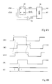
- FIG. 4A is intended to illustrate, using a simplified example with two clock signals CK1 and CK2, the principle of a circuit making it possible to provide an indication of phase relation.
- This circuit comprises a flip-flop RS 30 receiving on a "reset” input R the clock signal CK1 and on an “reset” input S the clock signal CK2.
- a direct output Q of the rocker When a 1 is present on input S and a 0 on input R, a direct output Q of the rocker is set to 1 and an inverted output Q * to 0. When a 1 is present on input R and a 0 on the input S, the direct output Q is set to 0 and the inverted output Q * to 1. When the states on the inputs R and S are identical, the flip-flop retains its state. The signal on the direct output Q is noted Q2 / 1 and the signal on the inverted output Q * is noted Q1 / 2.
- the output Q1 / 2 indicates by switching to 1 after a rising edge of the signal CK1, that the signal CK1 is in phase advance with respect to the signal CK2.
- the output Q2 / 1 is the logical inverse of the output Q1 / 2, and indicates, if it switches to 1 after a rising edge of the signal CK2, that the signal CK2 is in phase advance compared to the signal CK1.
- the outputs Q2 / 1 and Q1 / 2 are stored in a register 32 in order to continuously supply the phase relationship between the clocks CK1 and CK2.
- the register 32 is validated by the output EN of an AND gate 34 receiving the signals CK1 and CK2.
- the outputs Q1 / 2 and Q2 / 1 stored in register 32 are designated respectively by the references H1 and H2.
- FIG. 4B represents a timing diagram of the operation of the circuit of FIG. 4A.
- a rising edge of the signal CK1 occurs which is in phase deviation with respect to the signal CK2.
- the signals CK2, Q1 / 2, and EN are at 0.
- the signal H1 is in any state. This rising edge of the signal CK1 causes, after a propagation delay, the switching to 1 of the output Q1 / 2 (and the switching to 0 of the output Q2 / 1).
- the signal H1 remains at 1 to indicate this phase relationship continuously.
- the signal H2 remains at 0 to indicate that the signal CK2 is delayed in phase with respect to the signal CK1. If, over time, the phase relationship between the signals CK1 and CK2 is reversed, the states of the signals H1 and H2 are reversed, as described for time t2, to indicate this new phase relationship.
- FIG. 5 represents an embodiment of a circuit making it possible to indicate, among n clock signals CK1 to CKn, the two signals having respectively the maximum delay and the minimum delay.
- a flip-flop 30 receiving on its setting input 0 R a signal CKi and on its setting input 1 S a signal CKj provides on its direct output a signal Qj / i, and on its inverted output a signal Qi / j.
- a signal Qi / j indicates by switching to 1 after a rising edge of the signal CKi, that the signal CKi is in phase advance with respect to the signal CKj.
- the signal Lp is activated when each flip-flop 30 receiving the clock signal CKp indicates by one of its outputs Q that the signal CKp is delayed in phase with respect to the other clock signal that the flip-flop receives.
- an Hq signal is activated when each flip-flop 30 receiving the clock signal CKq indicates by one of its outputs Q that the clock signal CKq is in phase advance with respect to the other clock signal which the flip-flop receives.
- the registers 50 and 54 are validated after each last rising edge of the signals CK1 to CKn, for example by the output EN of an AND gate 58 receiving the signals CK1 to CKn.
- the indication circuit of FIG. 5 presents numerous applications other than those which will be described below. It can be used with any set of signals with a certain repetition of variation over time and which are such that the active edge of the most late signal occurs before an inactive edge of the most early signal.
- the circuit can, for example, be used to detect the first request from a set of requests of the same priority arriving at a microprocessor. By using multiplexers suitably controlled by the signals L1 to Ln and H1 to Hn, the circuit can supply the clock signal having the maximum phase advance and / or the clock signal having the maximum phase delay.
- FIG. 6 represents an embodiment of the circuit according to the invention making it possible to adjust the phase shifts between the clock signals CKl to CKn to a minimum value.
- This circuit is designed to detect the clock signal having the maximum phase delay and to increase the output impedances of the amplifiers (FIG. 1) supplying the other clock signals, so as to bring the phases of these other clock signals to a value close to the maximum delay. Indeed, by increasing the impedance of an amplifier, we decrease the slope of the edges of the clock signal which it supplies, which corresponds to increasing the phase delay of this clock signal.
- Each of the clock signals CK1 to CKn is delivered by a respective amplifier 60 with adjustable output impedance.
- Amplifiers 60 receive a common clock signal CK0.
- the output impedances of the amplifiers 60 are adjusted by respective signals C1 to Cn delivered by a control circuit 62 taking into account the states of n lines R1 to Rn.
- This control circuit is clocked by the global clock signal CK0, for example.
- the states of the lines R constitute the result supplied by a comparison circuit 64 receiving the clock signals CK1 to CKn.
- This comparison circuit 64 an embodiment of which is described below in relation to FIG. 7, and the control circuit 62 receive an initialization signal RST.
- the results R supplied by the comparison circuit 64 are established in the following manner, following an initialization RST.
- the control circuit 62 is provided for gradually increasing the output impedance of the amplifier 60 associated with each signal CKj until the line Rj switches to 0, indicating then that the clock signal CKj is delayed by phase with respect to the clock signal CKp.
- the impedances of the amplifiers 60 are increased by successive steps after they are initialized, by the signal RST, to their minimum values.
- the control circuit 62 to increase an impedance per step, supplies as many pulses as steps on the appropriate control line C (C1 to Cn).
- Such a control circuit can easily be made by a person skilled in the art using logic gates.
- Each signal Ci for example, is supplied by an AND gate receiving the signal Ri and the clock signal CK0.
- an adjustment phase when all the lines R are at 0, the clock signals which were in phase advance with respect to the signal CKp are all in phase delay with respect to the signal CKp.
- Such an adjustment phase is carried out on each activation of the initialization signal RST. This signal is activated when the circuit is energized, for example, or periodically.
- FIG. 7 represents an embodiment of comparison circuit 64.
- This circuit comprises an indication circuit 70 such as that described in relation to FIG. 5.
- the lines L1 to Ln indicating the clock signal having the delay of maximum phase, are supplied to a register 72 validated by the signal RST.
- n and j ⁇ p respectively receive the outputs Qj / p flip-flops 30 of the indication circuit 70.
- the outputs of the three-state doors 74 are merged into n lines connected to the input of a register 76.
- This register 76 is validated by the signal EN supplied by the indication circuit 70 and contains the result R above.
- each other result line Rj is set to the state of the output Qj / p which indicates that the signal CKj is in phase advance or not with respect to the CKp signal.
- FIG. 8 represents an embodiment of amplifier 60 with adjustable output impedance supplying a clock signal CKi.
- This amplifier includes a first inverter consisting of a P-channel MOS transistor MP1 and an N-channel MOS transistor MN1, the drains of which are connected respectively to a high potential Vcc and to a low potential Vss, the sources of which are connected together to form the output of the inverter, and the gates of which are connected together to form the input of the inverter, receiving the signal CK0.
- a plurality of additional inverters are provided, formed of P-channel MOS transistors MP2 and N-channel MOS transistors MN2, which can be connected in parallel to the inverter MP1 / MN1 or else disconnected.
- the sources of the transistors MP2 are connected to the potential Vcc and the sources of the transistors MN2 are connected to the potential Vss.
- the drains of the transistors MP2 and MN2 are connected to the clock output CKi by switches KP and KN respectively.
- the two switches KP and KN of each inverter MP2 / MN2 are controlled by a respective bit of a register 80.
- the register 80 is configured either as a shift register or as a counter.
- the content of register 80 is initialized by the signal RST so that all of the MP2 / MN2 inverters are connected in parallel to the MP1 / MN1 inverter, i.e. so that the output impedance of the amplifier 60 is minimal.
- the transistors MP2 are all the same size and the transistors MN2 the same.
- successive pulses of the control signal Ci introduce successive 1s in the shift register 80, so as to disconnect an inverter MP2 / MN2 at each pulse.
- register 80 is a counter, this is successively incremented by pulses of the control signal Ci.
- the transistors of the inverter MP2 / MN2 associated with the bit of rank 0 of register 80 have a given surface and the transistors of an inverter MP2 / MN2 associated with the bit of rank i of the register 80 have an area 2 i times greater.
Landscapes
- Engineering & Computer Science (AREA)
- Physics & Mathematics (AREA)
- General Engineering & Computer Science (AREA)
- General Physics & Mathematics (AREA)
- Theoretical Computer Science (AREA)
- Nonlinear Science (AREA)
- Manipulation Of Pulses (AREA)
- Stabilization Of Oscillater, Synchronisation, Frequency Synthesizers (AREA)
- Tests Of Electronic Circuits (AREA)
Applications Claiming Priority (2)
| Application Number | Priority Date | Filing Date | Title |
|---|---|---|---|
| FR9312452 | 1993-10-11 | ||
| FR9312452A FR2711287B1 (fr) | 1993-10-11 | 1993-10-11 | Circuit d'indication de relation de phase entre plusieurs signaux de même fréquence et son application à un circuit d'ajustage des déphasages entre ces signaux. |
Publications (2)
| Publication Number | Publication Date |
|---|---|
| EP0648018A1 true EP0648018A1 (de) | 1995-04-12 |
| EP0648018B1 EP0648018B1 (de) | 1998-07-01 |
Family
ID=9451994
Family Applications (1)
| Application Number | Title | Priority Date | Filing Date |
|---|---|---|---|
| EP94410085A Expired - Lifetime EP0648018B1 (de) | 1993-10-11 | 1994-10-10 | Schaltung zur Anzeige der Phasenverhältnisse zwischen mehreren Signalen mit gleicher Frequenz und ihre Anwendung in einer Schaltung zur Korrektur der Phasen zwischen diesen Signalen |
Country Status (5)
| Country | Link |
|---|---|
| US (1) | US5568072A (de) |
| EP (1) | EP0648018B1 (de) |
| JP (1) | JP2959972B2 (de) |
| DE (1) | DE69411346T2 (de) |
| FR (1) | FR2711287B1 (de) |
Families Citing this family (3)
| Publication number | Priority date | Publication date | Assignee | Title |
|---|---|---|---|---|
| JP3557275B2 (ja) | 1995-03-29 | 2004-08-25 | 株式会社ルネサステクノロジ | 半導体集積回路装置及びマイクロコンピュータ |
| US5880612A (en) * | 1996-10-17 | 1999-03-09 | Samsung Electronics Co., Ltd. | Signal de-skewing using programmable dual delay-locked loop |
| US6404240B1 (en) * | 2000-10-30 | 2002-06-11 | Semiconductor Components Industries Llc | Circuit and method of a three state phase frequency lock detector |
Citations (2)
| Publication number | Priority date | Publication date | Assignee | Title |
|---|---|---|---|---|
| US4639615A (en) * | 1983-12-28 | 1987-01-27 | At&T Bell Laboratories | Trimmable loading elements to control clock skew |
| US5036230A (en) * | 1990-03-01 | 1991-07-30 | Intel Corporation | CMOS clock-phase synthesizer |
Family Cites Families (10)
| Publication number | Priority date | Publication date | Assignee | Title |
|---|---|---|---|---|
| JPS5953515B2 (ja) * | 1976-10-25 | 1984-12-25 | 株式会社日立製作所 | 時間差検出回路 |
| US4604582A (en) * | 1985-01-04 | 1986-08-05 | Lockheed Electronics Company, Inc. | Digital phase correlator |
| US5087829A (en) * | 1988-12-07 | 1992-02-11 | Hitachi, Ltd. | High speed clock distribution system |
| JP2522413B2 (ja) * | 1989-10-17 | 1996-08-07 | 日本電気株式会社 | 位相周波数比較器 |
| US5164677A (en) * | 1990-01-16 | 1992-11-17 | Digital Equipment Corporation | Method and apparatus for synchronizing signals |
| US5118975A (en) * | 1990-03-05 | 1992-06-02 | Thinking Machines Corporation | Digital clock buffer circuit providing controllable delay |
| DE69130043T2 (de) * | 1990-09-18 | 1999-04-15 | Fujitsu Ltd., Kawasaki, Kanagawa | Elektronische Anordnung mit einem Bezugsverzögerungsgenerator |
| CA2071264C (en) * | 1991-06-18 | 1999-11-30 | Perry W. Lou | Regulated delay line |
| US5146121A (en) * | 1991-10-24 | 1992-09-08 | Northern Telecom Limited | Signal delay apparatus employing a phase locked loop |
| JP3455982B2 (ja) * | 1993-01-14 | 2003-10-14 | 株式会社デンソー | 偶数段リングオシレータ及びパルス位相差符号化回路 |
-
1993
- 1993-10-11 FR FR9312452A patent/FR2711287B1/fr not_active Expired - Fee Related
-
1994
- 1994-10-03 US US08/317,132 patent/US5568072A/en not_active Expired - Lifetime
- 1994-10-07 JP JP6243610A patent/JP2959972B2/ja not_active Expired - Fee Related
- 1994-10-10 EP EP94410085A patent/EP0648018B1/de not_active Expired - Lifetime
- 1994-10-10 DE DE69411346T patent/DE69411346T2/de not_active Expired - Fee Related
Patent Citations (2)
| Publication number | Priority date | Publication date | Assignee | Title |
|---|---|---|---|---|
| US4639615A (en) * | 1983-12-28 | 1987-01-27 | At&T Bell Laboratories | Trimmable loading elements to control clock skew |
| US5036230A (en) * | 1990-03-01 | 1991-07-30 | Intel Corporation | CMOS clock-phase synthesizer |
Non-Patent Citations (1)
| Title |
|---|
| "Low-Cost Clock Generation Circuit.", IBM TECHNICAL DISCLOSURE BULLETIN, vol. 30, no. 11, April 1988 (1988-04-01), ARMONK, US, pages 394 - 396 * |
Also Published As
| Publication number | Publication date |
|---|---|
| JPH07181233A (ja) | 1995-07-21 |
| FR2711287B1 (fr) | 1996-01-05 |
| JP2959972B2 (ja) | 1999-10-06 |
| DE69411346D1 (de) | 1998-08-06 |
| DE69411346T2 (de) | 1999-02-25 |
| EP0648018B1 (de) | 1998-07-01 |
| FR2711287A1 (fr) | 1995-04-21 |
| US5568072A (en) | 1996-10-22 |
Similar Documents
| Publication | Publication Date | Title |
|---|---|---|
| EP0645888B1 (de) | Digitale Verzögerungsleitung | |
| EP0648017B1 (de) | Vorrichtung zur Überwachung der Phasenverschiebung zwischen zwei Taktsignalen | |
| FR2827684A1 (fr) | Controleur de memoire presentant une capacite d'ecriture 1x/mx | |
| FR2563955A1 (fr) | Circuit retardateur de signaux numeriques | |
| FR2788902A1 (fr) | Boucles a retard asservies et procedes qui dephasent un signal d'horloge retarde en fonction d'une valeur de phase de reference | |
| EP0306392B1 (de) | Abfühlschaltung für Adressenumschaltungen | |
| FR2781940A1 (fr) | Amplificateur dont la sortance varie en fonction du temps | |
| FR2768276A1 (fr) | Generateur d'alea | |
| FR2664080A1 (fr) | Circuit de pilotage d'ecriture ayant des moyens de precharge. | |
| EP3376670B1 (de) | Konfigurierbare verzögerungsleitung | |
| EP0648018B1 (de) | Schaltung zur Anzeige der Phasenverhältnisse zwischen mehreren Signalen mit gleicher Frequenz und ihre Anwendung in einer Schaltung zur Korrektur der Phasen zwischen diesen Signalen | |
| EP0863512B1 (de) | Doppelzugriffspeicher | |
| FR2849228A1 (fr) | Dispositif de transfert de donnees entre deux sous-systemes asynchrones disposant d'une memoire tampon | |
| FR2861848A1 (fr) | Systmeme et procede d'evaluation de la vitesse d'un circuit | |
| US6222408B1 (en) | Synchronous delay circuit | |
| FR2718272A1 (fr) | Mémoire vive vidéo et procédé pour fournir en sortie des données série. | |
| EP0715415A1 (de) | Vorrichtung zur Parallelserienwandlung von binären Daten mit hoher Datenrate | |
| EP0686977B1 (de) | Zelle für Schieberegister | |
| FR2898223A1 (fr) | Circuit de distribution d'un signal initial a structure en arbre protege contre les aleas logiques. | |
| FR2610154A1 (fr) | Generateur de signaux de cadencement, notamment pour les systemes informatises de test de circuits integres | |
| FR2534729A1 (fr) | Dispositif de traitement de signal utilisant des systemes de transfert de charge | |
| EP0707260A1 (de) | Asynchrone Speicheranordnung mit seriellem Zugriff und entsprechendes Speicher- und Leseverfahren | |
| EP1739567A1 (de) | Vorrichtung zur asynchronen Arbitration und Mikrokontroller, der eine solche Arbitrationsvorrichtung umfasst | |
| FR2720852A1 (fr) | Dispositif de détection de transition engendrant une impulsion de durée variable. | |
| EP0169089B1 (de) | Elementare Datenverarbeitungsvorrichtung |
Legal Events
| Date | Code | Title | Description |
|---|---|---|---|
| PUAI | Public reference made under article 153(3) epc to a published international application that has entered the european phase |
Free format text: ORIGINAL CODE: 0009012 |
|
| AK | Designated contracting states |
Kind code of ref document: A1 Designated state(s): DE FR GB IT |
|
| 17P | Request for examination filed |
Effective date: 19950915 |
|
| 17Q | First examination report despatched |
Effective date: 19961212 |
|
| GRAG | Despatch of communication of intention to grant |
Free format text: ORIGINAL CODE: EPIDOS AGRA |
|
| GRAG | Despatch of communication of intention to grant |
Free format text: ORIGINAL CODE: EPIDOS AGRA |
|
| GRAH | Despatch of communication of intention to grant a patent |
Free format text: ORIGINAL CODE: EPIDOS IGRA |
|
| GRAH | Despatch of communication of intention to grant a patent |
Free format text: ORIGINAL CODE: EPIDOS IGRA |
|
| GRAA | (expected) grant |
Free format text: ORIGINAL CODE: 0009210 |
|
| AK | Designated contracting states |
Kind code of ref document: B1 Designated state(s): DE FR GB IT |
|
| REF | Corresponds to: |
Ref document number: 69411346 Country of ref document: DE Date of ref document: 19980806 |
|
| GBT | Gb: translation of ep patent filed (gb section 77(6)(a)/1977) |
Effective date: 19980903 |
|
| RAP4 | Party data changed (patent owner data changed or rights of a patent transferred) |
Owner name: STMICROELECTRONICS S.A. |
|
| PLBE | No opposition filed within time limit |
Free format text: ORIGINAL CODE: 0009261 |
|
| STAA | Information on the status of an ep patent application or granted ep patent |
Free format text: STATUS: NO OPPOSITION FILED WITHIN TIME LIMIT |
|
| 26N | No opposition filed | ||
| REG | Reference to a national code |
Ref country code: GB Ref legal event code: IF02 |
|
| PGFP | Annual fee paid to national office [announced via postgrant information from national office to epo] |
Ref country code: DE Payment date: 20031023 Year of fee payment: 10 |
|
| PG25 | Lapsed in a contracting state [announced via postgrant information from national office to epo] |
Ref country code: DE Free format text: LAPSE BECAUSE OF NON-PAYMENT OF DUE FEES Effective date: 20050503 |
|
| PGFP | Annual fee paid to national office [announced via postgrant information from national office to epo] |
Ref country code: FR Payment date: 20050825 Year of fee payment: 12 |
|
| PGFP | Annual fee paid to national office [announced via postgrant information from national office to epo] |
Ref country code: GB Payment date: 20051005 Year of fee payment: 12 |
|
| PG25 | Lapsed in a contracting state [announced via postgrant information from national office to epo] |
Ref country code: IT Free format text: LAPSE BECAUSE OF NON-PAYMENT OF DUE FEES;WARNING: LAPSES OF ITALIAN PATENTS WITH EFFECTIVE DATE BEFORE 2007 MAY HAVE OCCURRED AT ANY TIME BEFORE 2007. THE CORRECT EFFECTIVE DATE MAY BE DIFFERENT FROM THE ONE RECORDED. Effective date: 20051010 |
|
| GBPC | Gb: european patent ceased through non-payment of renewal fee |
Effective date: 20061010 |
|
| REG | Reference to a national code |
Ref country code: FR Ref legal event code: ST Effective date: 20070629 |
|
| PG25 | Lapsed in a contracting state [announced via postgrant information from national office to epo] |
Ref country code: GB Free format text: LAPSE BECAUSE OF NON-PAYMENT OF DUE FEES Effective date: 20061010 |
|
| PG25 | Lapsed in a contracting state [announced via postgrant information from national office to epo] |
Ref country code: FR Free format text: LAPSE BECAUSE OF NON-PAYMENT OF DUE FEES Effective date: 20061031 |