EP0641049B1 - Dispositif optique à semi-conducteur et sa méthode de fabrication - Google Patents
Dispositif optique à semi-conducteur et sa méthode de fabrication Download PDFInfo
- Publication number
- EP0641049B1 EP0641049B1 EP94306456A EP94306456A EP0641049B1 EP 0641049 B1 EP0641049 B1 EP 0641049B1 EP 94306456 A EP94306456 A EP 94306456A EP 94306456 A EP94306456 A EP 94306456A EP 0641049 B1 EP0641049 B1 EP 0641049B1
- Authority
- EP
- European Patent Office
- Prior art keywords
- layer
- region
- waveguide
- optical
- layers
- Prior art date
- Legal status (The legal status is an assumption and is not a legal conclusion. Google has not performed a legal analysis and makes no representation as to the accuracy of the status listed.)
- Expired - Lifetime
Links
Images












Classifications
-
- G—PHYSICS
- G02—OPTICS
- G02B—OPTICAL ELEMENTS, SYSTEMS OR APPARATUS
- G02B6/00—Light guides; Structural details of arrangements comprising light guides and other optical elements, e.g. couplings
- G02B6/10—Light guides; Structural details of arrangements comprising light guides and other optical elements, e.g. couplings of the optical waveguide type
- G02B6/12—Light guides; Structural details of arrangements comprising light guides and other optical elements, e.g. couplings of the optical waveguide type of the integrated circuit kind
- G02B6/12004—Combinations of two or more optical elements
-
- G—PHYSICS
- G02—OPTICS
- G02B—OPTICAL ELEMENTS, SYSTEMS OR APPARATUS
- G02B6/00—Light guides; Structural details of arrangements comprising light guides and other optical elements, e.g. couplings
- G02B6/24—Coupling light guides
- G02B6/26—Optical coupling means
- G02B6/30—Optical coupling means for use between fibre and thin-film device
- G02B6/305—Optical coupling means for use between fibre and thin-film device and having an integrated mode-size expanding section, e.g. tapered waveguide
-
- H—ELECTRICITY
- H01—ELECTRIC ELEMENTS
- H01S—DEVICES USING THE PROCESS OF LIGHT AMPLIFICATION BY STIMULATED EMISSION OF RADIATION [LASER] TO AMPLIFY OR GENERATE LIGHT; DEVICES USING STIMULATED EMISSION OF ELECTROMAGNETIC RADIATION IN WAVE RANGES OTHER THAN OPTICAL
- H01S5/00—Semiconductor lasers
- H01S5/02—Structural details or components not essential to laser action
- H01S5/026—Monolithically integrated components, e.g. waveguides, monitoring photo-detectors, drivers
-
- G—PHYSICS
- G02—OPTICS
- G02B—OPTICAL ELEMENTS, SYSTEMS OR APPARATUS
- G02B6/00—Light guides; Structural details of arrangements comprising light guides and other optical elements, e.g. couplings
- G02B6/10—Light guides; Structural details of arrangements comprising light guides and other optical elements, e.g. couplings of the optical waveguide type
- G02B6/12—Light guides; Structural details of arrangements comprising light guides and other optical elements, e.g. couplings of the optical waveguide type of the integrated circuit kind
- G02B2006/12083—Constructional arrangements
- G02B2006/12128—Multiple Quantum Well [MQW]
-
- G—PHYSICS
- G02—OPTICS
- G02B—OPTICAL ELEMENTS, SYSTEMS OR APPARATUS
- G02B6/00—Light guides; Structural details of arrangements comprising light guides and other optical elements, e.g. couplings
- G02B6/10—Light guides; Structural details of arrangements comprising light guides and other optical elements, e.g. couplings of the optical waveguide type
- G02B6/12—Light guides; Structural details of arrangements comprising light guides and other optical elements, e.g. couplings of the optical waveguide type of the integrated circuit kind
- G02B2006/12166—Manufacturing methods
- G02B2006/12195—Tapering
-
- H—ELECTRICITY
- H01—ELECTRIC ELEMENTS
- H01S—DEVICES USING THE PROCESS OF LIGHT AMPLIFICATION BY STIMULATED EMISSION OF RADIATION [LASER] TO AMPLIFY OR GENERATE LIGHT; DEVICES USING STIMULATED EMISSION OF ELECTROMAGNETIC RADIATION IN WAVE RANGES OTHER THAN OPTICAL
- H01S5/00—Semiconductor lasers
- H01S5/02—Structural details or components not essential to laser action
- H01S5/026—Monolithically integrated components, e.g. waveguides, monitoring photo-detectors, drivers
- H01S5/0265—Intensity modulators
-
- H—ELECTRICITY
- H01—ELECTRIC ELEMENTS
- H01S—DEVICES USING THE PROCESS OF LIGHT AMPLIFICATION BY STIMULATED EMISSION OF RADIATION [LASER] TO AMPLIFY OR GENERATE LIGHT; DEVICES USING STIMULATED EMISSION OF ELECTROMAGNETIC RADIATION IN WAVE RANGES OTHER THAN OPTICAL
- H01S5/00—Semiconductor lasers
- H01S5/10—Construction or shape of the optical resonator, e.g. extended or external cavity, coupled cavities, bent-guide, varying width, thickness or composition of the active region
- H01S5/1003—Waveguide having a modified shape along the axis, e.g. branched, curved, tapered, voids
- H01S5/1014—Tapered waveguide, e.g. spotsize converter
-
- H—ELECTRICITY
- H01—ELECTRIC ELEMENTS
- H01S—DEVICES USING THE PROCESS OF LIGHT AMPLIFICATION BY STIMULATED EMISSION OF RADIATION [LASER] TO AMPLIFY OR GENERATE LIGHT; DEVICES USING STIMULATED EMISSION OF ELECTROMAGNETIC RADIATION IN WAVE RANGES OTHER THAN OPTICAL
- H01S5/00—Semiconductor lasers
- H01S5/10—Construction or shape of the optical resonator, e.g. extended or external cavity, coupled cavities, bent-guide, varying width, thickness or composition of the active region
- H01S5/1053—Comprising an active region having a varying composition or cross-section in a specific direction
- H01S5/106—Comprising an active region having a varying composition or cross-section in a specific direction varying thickness along the optical axis
-
- H—ELECTRICITY
- H01—ELECTRIC ELEMENTS
- H01S—DEVICES USING THE PROCESS OF LIGHT AMPLIFICATION BY STIMULATED EMISSION OF RADIATION [LASER] TO AMPLIFY OR GENERATE LIGHT; DEVICES USING STIMULATED EMISSION OF ELECTROMAGNETIC RADIATION IN WAVE RANGES OTHER THAN OPTICAL
- H01S5/00—Semiconductor lasers
- H01S5/10—Construction or shape of the optical resonator, e.g. extended or external cavity, coupled cavities, bent-guide, varying width, thickness or composition of the active region
- H01S5/1053—Comprising an active region having a varying composition or cross-section in a specific direction
- H01S5/1064—Comprising an active region having a varying composition or cross-section in a specific direction varying width along the optical axis
-
- H—ELECTRICITY
- H01—ELECTRIC ELEMENTS
- H01S—DEVICES USING THE PROCESS OF LIGHT AMPLIFICATION BY STIMULATED EMISSION OF RADIATION [LASER] TO AMPLIFY OR GENERATE LIGHT; DEVICES USING STIMULATED EMISSION OF ELECTROMAGNETIC RADIATION IN WAVE RANGES OTHER THAN OPTICAL
- H01S5/00—Semiconductor lasers
- H01S5/20—Structure or shape of the semiconductor body to guide the optical wave ; Confining structures perpendicular to the optical axis, e.g. index or gain guiding, stripe geometry, broad area lasers, gain tailoring, transverse or lateral reflectors, special cladding structures, MQW barrier reflection layers
-
- H—ELECTRICITY
- H01—ELECTRIC ELEMENTS
- H01S—DEVICES USING THE PROCESS OF LIGHT AMPLIFICATION BY STIMULATED EMISSION OF RADIATION [LASER] TO AMPLIFY OR GENERATE LIGHT; DEVICES USING STIMULATED EMISSION OF ELECTROMAGNETIC RADIATION IN WAVE RANGES OTHER THAN OPTICAL
- H01S5/00—Semiconductor lasers
- H01S5/20—Structure or shape of the semiconductor body to guide the optical wave ; Confining structures perpendicular to the optical axis, e.g. index or gain guiding, stripe geometry, broad area lasers, gain tailoring, transverse or lateral reflectors, special cladding structures, MQW barrier reflection layers
- H01S5/22—Structure or shape of the semiconductor body to guide the optical wave ; Confining structures perpendicular to the optical axis, e.g. index or gain guiding, stripe geometry, broad area lasers, gain tailoring, transverse or lateral reflectors, special cladding structures, MQW barrier reflection layers having a ridge or stripe structure
- H01S5/227—Buried mesa structure ; Striped active layer
- H01S5/2272—Buried mesa structure ; Striped active layer grown by a mask induced selective growth
-
- H—ELECTRICITY
- H01—ELECTRIC ELEMENTS
- H01S—DEVICES USING THE PROCESS OF LIGHT AMPLIFICATION BY STIMULATED EMISSION OF RADIATION [LASER] TO AMPLIFY OR GENERATE LIGHT; DEVICES USING STIMULATED EMISSION OF ELECTROMAGNETIC RADIATION IN WAVE RANGES OTHER THAN OPTICAL
- H01S5/00—Semiconductor lasers
- H01S5/30—Structure or shape of the active region; Materials used for the active region
- H01S5/34—Structure or shape of the active region; Materials used for the active region comprising quantum well or superlattice structures, e.g. single quantum well [SQW] lasers, multiple quantum well [MQW] lasers or graded index separate confinement heterostructure [GRINSCH] lasers
- H01S5/3428—Structure or shape of the active region; Materials used for the active region comprising quantum well or superlattice structures, e.g. single quantum well [SQW] lasers, multiple quantum well [MQW] lasers or graded index separate confinement heterostructure [GRINSCH] lasers layer orientation perpendicular to the substrate
-
- Y—GENERAL TAGGING OF NEW TECHNOLOGICAL DEVELOPMENTS; GENERAL TAGGING OF CROSS-SECTIONAL TECHNOLOGIES SPANNING OVER SEVERAL SECTIONS OF THE IPC; TECHNICAL SUBJECTS COVERED BY FORMER USPC CROSS-REFERENCE ART COLLECTIONS [XRACs] AND DIGESTS
- Y10—TECHNICAL SUBJECTS COVERED BY FORMER USPC
- Y10S—TECHNICAL SUBJECTS COVERED BY FORMER USPC CROSS-REFERENCE ART COLLECTIONS [XRACs] AND DIGESTS
- Y10S438/00—Semiconductor device manufacturing: process
- Y10S438/942—Masking
Definitions
- the present invention relates to an optical semiconductor device and a method of manufacturing the same and more particularly to an optical semiconductor device having a high output semiconductor laser used for a light source of an information processing unit such as an optical printer and an optical disk unit, a semiconductor laser amplifier used for light amplification, an optical active element such as a semiconductor laser used in a transmitter of an optical communication apparatus or a photodiode used in a receiver thereof and an optical waveguide, and a method of manufacturing the same.
- DFB distributed feedback
- DBR distributed Bragg reflector
- a mode transducer is a mechanism for narrowing an output beam of a semiconductor laser originally having an output angle as wide as 30 to 40 degrees, and for facilitating optical coupling in the case in which a semiconductor laser and an optical fiber are formed into a module.
- the light spot diameter gets smaller, however, coupling with the optical fiber becomes more difficult.
- a semiconductor laser requiring a high output such as a laser for exciting a fiber type optical amplifier using an optical fiber doped with erbium or a semiconductor laser for writing information in a optical disk, suffers from the problem that an optical power density rises at a laser end face and damage to the end face is liable to be caused.
- a semiconductor laser amplifier may have the drawback that the optical output is saturated easily when beam confinement is intense.
- Photodiodes that have a rapid speed of response and a high quantum efficiency are required, and furthermore, photodiodes that can be formed into a thin shape and that can permit convenient electrical wiring are demanded.
- An end face incidence waveguide type photodiode is available as a photodiode which meets these requirements.
- reactive components of light absorption such as free carrier absorption of a cladding layer are reduced so that the quantum efficiency is increased, thus improving sensitivity.
- a semiconductor laser, a semiconductor laser amplifier, and a photodiode having an optical waveguide in which beam confinement is intense inside and beam confinement is weak at an end face,are demanded in the fields of optical communication and optical information processing.
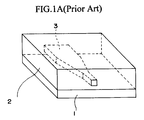
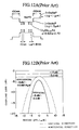
- FIG. 1A to FIG. 1C waveguides for converting an optical beam diameter composed of a semiconductor have been proposed as shown in FIG. 1A to FIG. 1C.
- the semiconductor waveguide shown in FIG. 1A is disclosed in [1] the Institute of Electronic Information Communications in Japan, National Autumn Meeting 1992, Lecture Number C-201 for example.
- the semiconductor waveguide shown in FIGs. 1B and 1C has been proposed in [2] the Institute of Electronic Information Communications in Japan, National Autumn Meeting 1992, Lecture Number C-202 for instance.
- [3] T.L. KOCH et al., IEEE PHOTONICS TECHNOLOGY LETTERS, VOL. 2, NO. 2, 1990 another semiconductor waveguide is proposed in a mode transducer integrated Fabry-Pérot semiconductor laser (hereinafter referred to also as an FP-LD) having a waveguide for converting an optical beam diameter.
- FP-LD mode transducer integrated Fabry-Pérot semiconductor laser
- the optical beam diameter converting waveguide shown in FIG. 1A has an InGaAsP core layer 3 surrounded by an InP substrate 1 and an InP cladding layer 2 at top and bottom and left and right.
- the lateral dimension (width) of the InGaAsP core layer 3 is wide at one end face and gets narrower with greater proximity to the opposite end face, and the optical beam diameter spreads in the lateral direction with greater proximity to the said opposite end face (where the width of the core layer is narrowed) in accordance with the variation of the core-layer width.
- the thickness of the InGaAsP core layer 3 is uniform, and the plane pattern thereof is formed by lithography technique using an exposure mask.
- the semiconductor waveguide is effective for converting an optical beam diameter in a lateral direction, but the optical beam diameter in a longitudinal direction (a thickness direction of the layer) is not converted.
- the optical beam diameter in the thickness direction of the core layer is generally smaller than that in the width direction thereof, conversion of the optical beam diameter in the longitudinal direction is important for the improvement of the optical coupling efficiency with an optical fiber, an optical semiconductor element or the like. Since the optical beam diameter in the thickness direction of the layer is not converted in the semiconductor waveguide for converting the optical beam diameter shown in FIG. 1A, a significant effect cannot be expected as regards the improvement of the optical coupling efficiency between the semiconductor optical waveguide and an optical fiber or the like.
- a semiconductor waveguide used to convert the optical beam diameter, and a waveguide-shaped photodiode into an integral construction. Since the thickness and the composition of the core layers become uniform in the optical axis direction, however, the end face of the semiconductor waveguide also becomes a light absorption region and the optical loss is increased. Furthermore, since a PN junction is exposed at the end face, a dark current is increased. When the dark current is more or less increased, there is a problem that a signal-to-noise ratio may deteriorate undesirably, especially in a case in which very high sensitivity is required.
- the semiconductor waveguide for converting the optical beam diameter shown in FIGS. 1B and 1C has a construction that the optical beam diameter is converted in the thickness direction of the film.
- This semiconductor waveguide has a first InP cladding layer 5 laminated on an InP substrate 4, a multi-quantum well (MQW) layer 6 composed of an InP well and an InAlAs barrier formed thereon and a second InP cladding layer 7 formed on the MQW layer 6. Further, an InGaAsP core layer 8 is formed in the MQW layer 6, and the film thickness at one end thereof is reduced in the MQW layer 6. Besides, the MQW layer 6 serves as a cladding layer for the core layer 8 and as a core layer for the first and the second InP cladding layers 5 and 7. The core layer 8 is formed both in a gain region 9 and a mode conversion region 10. Further, the core layer 8 in the mode conversion region 10 is formed in a tapered shape in the thickness direction, and gets thinnerwith increasing distance from the gain region 9.
- MQW multi-quantum well
- the light advancing in such a semiconductor waveguide is confined in the MQW layer 6 and further confined more intensely in the cladding layer 7.
- the optical beam diameter is converted at a portion where the film thickness of the core layer 8 is changed.
- a near field pattern at a taper bottom end portion is spread.
- a far field pattern which is a diffracted pattern of the near field pattern is contracted. Accordingly, an output angle of a beam emitted from the taper bottom end is narrowed, which makes coupling with an optical fiber easier.
- Three cone-shaped patterns in FIG. 1C show intensity distribution of a photoelectric field.
- the core layer 8 shown in FIG. 1C has a structure in which an InGaAsP layer 8a and an InP layer 8b are laminated alternately as shown in an enlarged view led out from the main view with a dashed line, and the InGaAsP layers 8a and 8b are subject to stepwise patterning using the InP layer 8b as an etching stop layer, thus varying the film thickness of the core layer 8 in stepwise manner.
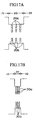
- the FP-LD described in the above-mentioned citation [3] is structured by forming a first InP cladding layer 102, a waveguide layer 103, a multiple quantum well (MQW) active layer 104 and a second InP cladding layer 105 one upon another on an InP substrate 101 as shown in FIG. 2.
- the MQW active layer 104 is structured of an InGaAs well layer and an InGaAsP barrier layer, and is formed only in a gain region 110.
- the waveguide layer 103 is formed in both the gain region 110 and a mode conversion region 111.
- a reference numeral 106 represents a contact layer formed on the second InP cladding layer 105
- 107 represents an etching stop layer formed in the second cladding layer.
- the waveguide layer 103 in the mode conversion region 111 is formed in a tapered form in the thickness direction, and gets thinner with greater distance from the gain region 110.
- the waveguide layer 103 has a structure in which an InGaAsP layer 103a and an InP layer 103b are laminated alternately. Further, the InP layer 103b is used as an etching stop layer, and the InGaAsP layer 103a and the InP layer 103b are subjected to patterning to form a step form while changing the etching proof mask a plurality of times, thus forming the film thickness of the waveguide layer 103 in the mode conversion region in a tapered form.
- the near field pattern thereof at the taper bottom end portion spreads since optical confinement is weaker in the mode conversion region 111 than that in the gain region 110, thus resulting in that the far field pattern that is a diffracted pattern of the near field pattern is narrowed. Accordingly, the output angle of a beam emitted from the taper bottom end is narrowed, thus making coupling with an optical fiber easier.
- the waveguide layer 103 forming a resonator has a construction in which the number of layers becomes less with greater proximity to the output end, and the tapered form of the waveguide layer 103 is obtainable by changing the etching-proof mask a plurality of times. Therefore, this construction is liable to include a crystal defect and adverse effects on the characteristics of a light emitting element are liable to be produced.
- the active layer 104 in the gain region 110 and the tapered waveguide layer 103 in the mode conversion region 111 are different layers and formed of almost the same composition in the construction described in the above-mentioned citation [3], a part of the laser light is liable to be absorbed in the portion near the gain region 110 of the tapered waveguide layer 103. Accordingly, lowering of an optical output and a slope efficiency (a differential value of a leading edge of a current to light intensity characteristic curve) is unavoidable as compared with a laser element in which the mode converter is not integrated.
- the tapered waveguide is located in a resonator in the FP-LD described in the citation [3], even the fundamental characteristics of the semiconductor laser can be affected, and a threshold current in pulse measurement rises up to 70 mA in an element having double end cleavage. Moreover, no report has been made that continuous oscillation has occurred at room temperature in an element having double end cleavage.
- the tapered form of the waveguide layer is obtained by means of an etching method, it becomes difficult to form the tapered form sufficiently uniformly from one device to the next, thus presenting the risk that the yield may be lowered in addition to poor controllability of the beam spot configuration. Moreover, a crystal defect is liable to be produced in the waveguide layer forming the resonator and adverse effects on the characteristics of a light emitting element are liable to be produced. Furthermore, the waveguide layer is composed of a single material, and does not have an MQW layer in a tapered form such as described in the citation [3].
- This device may be considered to include: a support structure having a semiconductor substrate; and a quantum well structure formed on the said support structure and having a stack of layers including at least one well layer and two barrier layers sandwiching the well layer, the said quantum well structure including an active optical region, forming at least part of the said active optical element, and also including a waveguide region having a first end adjacent to the said active optical region and a second end adjacent to an interface portion of the device at which an output optical beam is emitted from the device, or an input optical beam is received by the device, when the device is in use, the said waveguide region of the quantum well structure forming at least part of a core layer of the said waveguide and serving to couple the active optical element optically to the said interface portion when the device is in use, there being upper and lower cladding layers above and below the core layer respectively.
- a method of manufacturing the device may be considered to include: forming a masking film of dielectric material on an upper main face of a support structure including a semiconductor layer; patterning the masking film so as to expose respective first and second regions of said semiconductor layer of the said support structure, the said first region being elongate and the said second region having a first end adjoining one end of the said first region and a second end, of greater width than the said first region, adjacent to an intended interface portion of the finished device at which, in use of the said finished device, an output optical beam is to be emitted from the device or an input optical beam is to be received by the device; and forming layers successively over the first and second regions so as to provide over both regions a quantum well structure having a stack of the layers including at least one well layer and two barrier layers sandwiching the well layer, and so as to provide over at least the said second region upper and lower cladding layers above and below the said quantum well structure respectively, at least the said well layer being formed by a selective area growth method so that
- the quantum well structure is relatively thick in the active optical region in which a laser is formed and relatively thin in the waveguide region. There is a step change in thickness in a short boundary region between the active optical region and the waveguide region.
- EP-A-0495202 discloses a passive beam-converter arrangement for coupling a semiconductor optical element such as a laser to an optical conductor such as a monomode fiber.
- the arrangement has a first optical waveguide embedded in a second, larger optical waveguide.
- the first optical waveguide tapers as it extends into the second waveguide and ends at a distance from the end face of the second waveguide so that an optical wave propagating through the first waveguide spreads as a consequence of the reducing thickness of the first waveguide, until guidance of the wave is taken over by the second waveguide.
- an optical semiconductor device in which an active optical element and a waveguide are formed integrally, the device including: a support structure having a semiconductor substrate; and a quantum well structure formed on the said support structure and having a stack of layers including at least one well layer and two barrier layers sandwiching the well layer, the said quantum well structure being formed in an active optical region of the said active optical element, and also being formed in a waveguide region that has a first end adjacent to the said active optical region and that has a second end adjacent to an interface portion of the device at which an output optical beam is emitted from the device, or an input optical beam is received by the device, when the device is in use, the quantum well structure in the said waveguide region forming at least part of a core layer of the said waveguide and serving to couple the active optical element optically to the said interface portion when the device is in use, there being upper and lower cladding layers above and below the core layer respectively; characterised in that the thickness of the said well layer decreases gradually over the length of the said
- the active optical element such as a semiconductor laser, a light emitting diode or a photodiode
- the optical waveguide are formed in a monolithic manner, and the diameter of an optical beam in a thickness direction of the core layer at an end face of the optical waveguide can be suitably large for good coupling efficiency to an external optical conductor.
- the waveguide which serves as a mode converter, has reduced optical absorption
- the active optical element can, for example, perform stable laser oscillation at a low threshold.
- a part of the active optical element is constituted by one part (the active optical region) of the quantum well structure which has for example a stripe form, whilst another part (the waveguide region)of the same quantum well structure constitutes a part of the waveguide, and the quantum well structure in the waveguide region is made thinner with greater distance from the active optical region without changing the number of layers, thus converting the diameter of the optical beam.
- optical confinement gets weaker in the thickness direction of the core layer as the light goes toward the end portion (interface portion).
- the optical beam diameter gets larger.
- optical confinement becomes more intense as the light travels toward the active optical element, and the optical beam diameter gets smaller as it travels to reach the active optical element.
- the efficiency of optical coupling between the optical active element and the optical fiber is improved by going through the optical waveguide.
- the optical waveguide and the active optical element are formed as one body, positioning from the outside becomes unnecessary and so the optical coupling loss is reduced.
- an energy band gap of the core layer of the optical waveguide becomes larger with greater distance from the active optical element. Therefore, when the active optical element is a semiconductor laser or a semiconductor laser amplifier, the light having a laser-oscillated wavelength is not absorbed significantly by the optical waveguide and so the absorption loss in the optical semiconductor device is reduced.
- the optical beam diameter becomes larger at a distant position from the active optical element and becomes smaller at a near position therefrom.
- the coupling efficiency between the optical active element and the optical fiber is further improved by having the optical waveguide lie therebetween.
- the cladding layer of the optical waveguide is preferably formed with a non-doped semiconductor, so that light absorption by free carriers is reduced, thus controlling attenuation of light intensity. Further, when a cladding layer of the optical waveguide and a cladding layer of the optical active element are separated from each other by a groove the parasitic capacity of the active optical element can be reduced.
- the width of the waveguide core layer preferably increases gradually in the direction away from the active optical element so that a mode of the light expands in the width direction through the core layer of the optical waveguide, and hence the optical beam diameter in the width (lateral) direction can also be increased at the interface portion.
- the thickness of the quantum well structure in the waveguide region may be twice or more at the input end (first end) of the region than at the output end (second end). According to the foregoing, the shape of the beam spot emitted from the quantum well structure becomes a circle or a shape very close to a circle, and moreover, the beam output angle thereof falls within the range from 20 degrees to 10 degrees. Hence, the coupling efficiency with an optical fiber or the like is improved by a large margin.
- the waveguide region of the quantum well structure forming part of the waveguide for mode conversion, is thinner than the active optical region of the quantum well structure forming part of the active optical element and a ground level of the quantum well is higher in the waveguide for mode conversion than that in the active optical element.
- a light absorption wavelength edge in the waveguide for mode conversion at the output end portion (interface portion) has a shorter wavelength than the oscillation wavelength in the active optical element.
- a circular beam spot can be formed by forming the quantum well structure in a stripe shape and setting the ratio of minimum values of both end widths of the stripe-shaped quantum well structure to 0.8 to 1.2, thus making optical coupling with an optical fiber or the like easier.
- the film thickness of the quantum well structure gets thinner gradually from the end portion of the active optical region (gain region) to the light output end of the waveguide for mode conversion, there is a risk that a part of the waveguide for mode conversion in the vicinity of the gain region may become a saturable absorption layer, thus inflicting a serious loss.
- a current is applied locally by providing an electrode or extending a contact layer in a boundary region near the gain region in the waveguide for mode conversion, so that the boundary region becomes transparent reliably and significant light absorption does not occur.
- the electrode formed in the boundary region near the gain region in the waveguide for mode conversion may be obtained either by extending the electrode in the gain region or by forming it separately from the electrode in the gain region, but it is easier to control the light absorption quantity by using a separate electrode.
- a method of manufacturing an optical semiconductor device in which an active optical element and a waveguide are formed integrally including: forming a masking film of dielectric material on an upper main face of a support structure including a semiconductor substrate; patterning the masking film so as to expose respective first and second regions of semiconductor material of the said support structure, the said first region corresponding to an active optical region of the said active optical element and being elongate, and the said second region corresponding to a waveguide region and increasing gradually in width from a first end thereof adjoining one end of the said first region to a second end thereof adjacent to an intended interface portion of the finished device at which, in use of the said finished device, an output optical beam is to be emitted from the device or an input optical beam is to be received by the device; and forming layers successively over the first and second regions so as to provide over both regions a quantum well structure having a stack of the layers including at least one well layer and two barrier layers sandwiching the well layer, the quantum well structure over the said
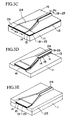
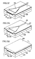
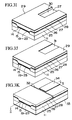
- FIG. 3A to FIG. 3K are perspective views showing a manufacturing process of a first optical semiconductor device according to an embodiment of the present invention.
- FIG. 4A and FIG. 4B are partial sectional views of the manufacturing process
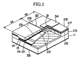
- FIG. 5 is a partly cut out perspective view of a completed optical semiconductor device.
- a diffraction grating 13 is formed by an interference exposure method in a region including a semiconductor laser forming region 12 on a surface of an n-InP substrate 11.
- the diffraction grating 13 is formed of irregularities repeated at a constant pitch in the waveguide direction.
- n-InGaAsP whose composition is specified by a wavelength ⁇ g of 1.5 ⁇ m showing the composition is accumulated in a thickness of 150 nm by an epitaxial growth method, thereby to form a guide layer 14. Furthermore, an n-InP buffer layer (cladding layer) 15 is formed thereon in a thickness of 10 nm to produce a support structure.
- a dielectric masking film 16 such as SiO 2 or Si x N y is formed on the support structure by a thermal CVD method and an opening is formed by a lithography method in the dielectric film 16 at the semiconductor laser forming region 12 and a waveguide forming region 17, thereby to form a spatula-shaped window 18.
- the configuration of the semiconductor laser forming region 12 is rectangle having a longer side in the waveguide direction.
- the waveguide forming region 17 has a shape obtained by combining a trapezium portion, in which the width thereof widens continuously at a constant angle with greater distance from the end portion of the semiconductor laser forming region 12, and a rectangular portion that is in contact with the base of the trapezium portion.
- the width W 1 of the window 18 at the end portion of the semiconductor laser forming region 12 (first end of the waveguide region) is 15 to 20 ⁇ m
- the width W 2 of the base of the trapezium portion (second end) of the waveguide forming region 17 is 150 to 200 ⁇ m.
- a first InGaAsP guide layer 19 is grown epitaxially, and an MQW layer (quantum well structure) 20 composed of three InGaAs well layers and InGaAsP barrier layers having a wavelength ⁇ g of 1.3 ⁇ m sandwiching the well layers therebetween, a second InGaAsP guide layer 21, a p-InP cladding layer 22 and an n-InGaAsP etching stop layer 23 are grown one after another epitaxially.
- MQW layer quantum well structure
- the layers 19 to 23 may be formed after the surface of the n-InP cladding layer 15 exposed from the window 18 is etched slightly. This etching is for purifying the surface of the cladding layer 15.
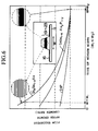
- These semiconductor layers 19 to 23 are not grown on the dielectric film 16 which has no growth nucleus, but are grown in the region of the window 18 selectively. Moreover, since the crystal growth speed becomes lower as the pattern width W of the window 18 gets larger, the film thickness of these semiconductor layers 19 to 23 depends on the pattern width W of the window 18, and the final film thickness becomes thin at the wide end (W 2 ) as shown in FIG. 6. Accordingly, the respective semiconductor layers 19 to 23 laminated on the buffer layer 15 through the window 18 are thickest in the semiconductor laser forming region 12 and get thinner gradually toward the bottom end portion of the waveguide forming region 17 from the end portions thereof.
- the thickness of an InGaAs well layer 20a and the thickness of an InGaAsP barrier layer 20b in the semiconductor laser forming region 12 are 6 nm and 16 nm, respectively
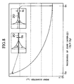
- the thickness of the InGaAs well layer 20a and the thickness of the InGaAsP barrier layer 20b at the bottom end portion of the waveguide forming region 17 become 1.5 nm and 4 nm, respectively. Therefore, the energy band thereof appears as shown in FIG. 7A in the semiconductor laser forming region 12 and appears as shown in FIG. 7B in the waveguide forming region 17, respectively.
- the film thickness of the guide layers 19 and 21 at the bottom end portion of the waveguide forming region 17 is set to 10 nm, and the film thickness of the p-InP cladding layer 22 and the film thickness in the semiconductor laser forming region 12 of the InGaAsP etching stop layer 23 areset to 500 nm and 10 nm, respectively.
- This mask pattern 24 has a configuration like a spatula exposing edge portions on both sides of the top of the etching stop layer 23.
- it is rectangular in shape (having the width W 3 of 1.5 pm) in the semiconductor laser forming region 12, and has a configuration obtained by putting together a trapezium, having a width W 4 of 8 um at the base, and a quadrilateral, extending from the trapezium base without varying in width, in the waveguide forming region 17.
- etching is applied continuously up to the etching stop layers 23 located on both sides of the mask pattern 24 and the top of the n-InP substrate 11, thus defining the final width of the semiconductor laser and the waveguide for converting optical beam diameter.
- the width of the active layer of the semiconductor laser becomes 1.5 ⁇ m, and that of the bottom end of the waveguide becomes 8 ⁇ m.
- an InP high resistance layer 25 doped with iron is formed by an epitaxial method on the n-InP substrate 11 exposed on both sides of the mask pattern 24 as shown in FIG. 3E. Then, as shown in FIG. 3F, an n-InP current block layer 26 and an InGaAsP etching stop layer 27 are grown epitaxially on the high resistance layer 25.
- FIG. 4A is a sectional view taken along a line I-I in FIG. 3H.
- the reason why non-doped InP is used instead of p-InP is to reduce light absorption by free carriers in the optical beam diameter conversion waveguide.
- a dielectric film 29 is formed, patterning is applied to this film 29 thereby to form a window 30 in the semiconductor laser forming region 12 and thereabout, and the InP cladding layer 28 exposed from the window 30 is etched selectively.
- the etching depth is controlled by the InGaAsP etching stop layers 23 and 27.
- a p-InP cladding layer 31 is grown epitaxially on the p-InP cladding layer 22 through the window 30 as shown in FIG. 3J, thereby to aim at levelling the cladding layer 31 and the non-doped InP cladding layer 28.
- patterning is applied to the non-doped InP cladding layer 28 and the p-InP cladding layer 22 below the layer 28, the InGaAsP etching stop layers 23 and 27 and the current block layer 26, thereby to form a groove 32 for separating the semiconductor laser forming region 12 and the waveguide forming region 17 from each other.
- the guide layer 21 is finally made to function as an etching stop layer.
- FIG. 4B is a sectional view taken along a line II-II in FIG. 3K.
- the width of the MQW layer 20 which becomes a core layer may be made constant. In this case, it is sufficient to set the width of the mask 24 in FIG. 3D constant, e.g., to W 3 .
- the above-mentioned semiconductor laser 35 oscillates by applying a current across the n-side electrode 33 and the p-side electrode 34, and, when the laser light is outputted to the optical beam diameter conversion waveguide 36, the laser light advances while being confined within the MQW layer 20.
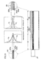
- the film thickness gets thinner with increasing distance from the semiconductor laser 35, and the optical beam diameter in the film thickness direction increases.
- the MQW layer 20 which is the core layer of the waveguide 36
- optical confinement gets weaker as the film thickness D thereof gets thinner.
- the light emitted from the MQW layer 20 (having a thickness of D 1 ) of the semiconductor laser 35 spreads out in the film thickness direction as it propagates towards the bottom end portion (having a thickness of D 2 ) of the optical beam diameter conversion waveguide 36.
- a photoelectric field intensity distribution P 1 in the semiconductor laser 35 has a sharp peak of intensity in the MQW layer 20
- a photoelectric field intensity distribution P 2 at the bottom end portion of the optical beam diameter conversion waveguide 36 has a broad spread, which is almost the same as that of a light intensity distribution P 3 of an optical fiber 37 connected to the end portion thereof.
- the energy band gap between a quantum level on the valence band side and a quantum level on a conductive band side becomes larger as the well layer gets thinner, and moreover, the energy band gap between the valence band and the conductive band becomes larger (Eg 1 ⁇ Eg 2 ) as the film thickness gets thinner as shown in FIG. 7A and FIG. 7B.
- Eg 1 ⁇ Eg 2 the energy band gap between the valence band and the conductive band becomes larger
- an edge of the absorption vs. wavelength characteristic for the end face of the optical beam diameter conversion waveguide 36 falls on the side shorter than a wavelength ⁇ 0 of the light outputted from the semiconductor laser 35 as shown in FIG. 10B. Therefore, the optical beam diameter conversion waveguide 36 does not absorb the light. As a result, attenuation of the light intensity in the optical beam diameter conversion waveguide 36 is reduced, and the intensity of the light outputted to the optical fiber 37 is increased.
- the refractive index of the MQW can be regarded as the average of the refractive indices, taking into account the thicknesses of the well layer and the barrier layer. Accordingly, the MQW layer 20 at the bottom end of the optical beam diameter conversion waveguide 36 has a refractive index smaller than that of the MQW layer 20 of the semiconductor laser 35, and the difference in the refractive index from the cladding layers 22 and 15 above and below the MQW layer 20 is reduced, thus enlarging the optical beam diameter.
- the width of the MQW layer 20 becomes wider towards the output end. Therefore, the beam diameter of the light confined therein also gets wider in the width (lateral) direction in accordance with the change of the width thereof.
- the MQW layer 20 gets thinner, optical confinement not only in the film thickness direction but also in the direction perpendicular to the film thickness (the lateral direction) gets weaker even if the width of the MQW layer 20 is fixed. Accordingly, the optical beam diameter spreads, thus improving the coupling efficiency.
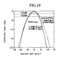
- the horizontal axis (abscissa) represents an offset between the respective central axes of the optical fiber 37 and the waveguide 36
- the vertical axis (ordinate) represents the coupling loss between the fiber and waveguide.
- a solid line shows the coupling loss in a vertical direction (the film thickness direction of the MQW layer)
- a dashed line shows the coupling loss in a horizontal direction (the width direction of the MQW layer).
- FIG. 13 Since it is desired to couple the above-mentioned optical semiconductor device with the optical fiber 37 without requiring any adjustment, an example thereof is shown in FIG. 13.
- a silicon wafer 41 is partitioned into a plurality of sections, and bonding pads 42 for fixing the optical semiconductor device shown in FIG. 5 and a V-shaped groove 43 for mounting the bottom end portion of the optical fiber 37 are formed in each section. Further, in a region where the optical semiconductor device is to be mounted, an extending electrode 44 to be connected to the p-side electrode 34 of the semiconductor laser 35 is formed.
- the V-shaped groove 43 is formed by etching the wafer 41 with a KOH solution through a window formed in a dielectric film 45 covering the surface of the silicon wafer 41. In this case, positions of the V-shaped groove 43 and the bonding pads 42 are set in advance so that the positions of the optical output portion of the optical semiconductor device and the V-shaped groove 43 coincide with each other.
- the optical fiber 37 is placed in the V-shaped groove 43 and fixed there, once the silicon wafer 41 has been partitioned into chip-form sections and the p-side electrode 34 of the semiconductor laser 35 has been connected to the extending electrode 44 and bonded onto the chips, thus completing the coupling.
- an electric field absorbing type optical modulator 40 may also be formed between the semiconductor laser 35 and the optical beam diameter conversion waveguide 36 by means of the separate p-side electrode 34A as shown in FIG. 9.
- the taper configuration in the mode converting region 17 of the MQW layer of the device is obtained by defining the shape of the mask which is used for growing a film, without changing the etching process, crystal defects are less likely to be produced in the part of MQW layer having the tapered form. As a result, less adverse effects on the characteristics arise from such crystal defects in this layer. Moreover, the taper configuration can be formed with small error and high yield, thus making it possible to obtain beam spots having a uniform configuration.
- a mask having a spatula-shaped window 18 such as shown in FIG. 3A is used in order to vary the film thickness of the semiconductor layers 19 to 23 forming the optical beam diameter conversion waveguide 36.
- the waveguide forming region 17 of the window 18 has the above-mentioned trapezium shape which widens uniformly at a fixed angle, but alternatively, as shown in Fig. 14, a window 38 having a pattern that widens in stepwise manner may also be formed by forming portions 38A to 38D where the width is not changed and spreading portions 38E to 38H alternately.
- the film thickness of the semiconductor layers 19 to 23 of the window optical beam diameter conversion waveguide 36 becomes thinner stepwise toward the bottom end portion as shown in FIG. 15, and the characteristic thereof is almost the same as that of the first embodiment.
- the width of the window 18 of the mask is changed by as many steps as possible.
- the variation of the thickness of the semiconductor layers may be made larger by making the variation of the width larger.
- a plurality of windows 38A are arranged at predetermined intervals in parallel with a dielectric film 16A in a configuration in which regions corresponding to the semiconductor beam forming regions 12 and optical beam diameter conversion waveguide regions 17 shown in FIG. 3A are connected in series repeatedly as shown in FIG. 16.
- a plurality of optical semiconductor devices each having a semiconductor laser and an optical beam diameter conversion waveguide are formed continuously on the substrate through a process such as that described hereinbefore with reference to the first embodiment. Thereupon, it is sufficient to cleave the substrate 11 along cut lines L 11 to L 14 and L 21 to L 26 so as to separate the individual optical semiconductor devices.
- the guide layers 19 and 21 are provided above and below the MQW layer 20 in the first embodiment described above, but a construction without these layers may also be adopted.
- the energy band thereof appears as shown in FIG. 17A and FIG. 17B.
- the well layer and the barrier layer become as thin as several nm near to the bottom end portion of the optical beam diameter conversion waveguide 36. Therefore, when the guide layers 19 and 21 are not provided, the difference of the refractive index in the width (lateral) direction may be too small and optical confinement becomes weaker.
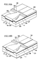
- a groove 32 for separating the optical semiconductor laser 35 from the optical beam diameter conversion waveguide 36 is filled with an insulating material 38 such as polyimide to be flattened, and then patterning is applied to the cladding layer 28 by a photolithography method with a dielectric film such as SiO 2 or SiN as a mask, thereby to form the ridge construction.
- An n-side electrode 33 and a p-side electrode 34 are formed thereafter as shown in FIG. 18B.
- the cladding layers 15, 22 and 28 above and below the MQW layer 20 which becomes the core layer are made of the same material as that of the semiconductor laser 35, but cladding layers 15A and 22A may be formed of a material such as InGaAsP having a refractive index smaller than that of the cladding layer of the semiconductor laser 35 as shown in FIG. 20.
- optical confinement in the optical beam diameter conversion waveguide 36 is reduced thus making it possible to make the optical beam diameter in the film thickness direction larger. Furthermore, when the cladding layers 15A and 22A are non-doped, light absorption by free carriers is reduced.
- an InGaAsP etching stop layer 23A is provided between the guide layer 21 and the cladding layer 22, thus adjusting the etching depth when the cladding layers 22 and 28 located in the optical beam diameter conversion waveguide 36 are removed, and an upper non-doped InGaAs cladding layer 22A is formed after the etching.
- a semiconductor laser is used as an active element connected to the optical beam diameter conversion waveguide in the first embodiment described above, but a photodiode may also be adopted.
- the element thereof When a reverse bias is applied to the semiconductor laser 35, the element thereof functions as an end face wave conductive type photodiode of a pin junction construction.
- a photodiode of pn junction and an end face light emitting type light emitting diode of pn junction or pin junction may also be used as an optical active element.
- the construction of the core layer of the optical beam diameter conversion waveguide connected to the photodiode or the light emitting diode is the same as that of the optical absorption layer or the active layer of the optical active element.
- the photodiode when it is formed in one body with the optical beam diameter conversion waveguide, it may also be arranged to form a recessed portion in a photodiode forming region and to form a photodiode therein as shown in FIG. 21 for instance.
- a dielectric mask having an almost spatula-shaped window similar to those shown in FIG. 3A and FIG. 15 for instance is used, and an n-InP cladding layer 54, an InGaAs core layer 55 and a non-doped InP cladding layer 56 are formed on the etching stop layer 53 through that window.
- the core layer 55 and the upper and lower cladding layers 54 and 56 are thick in the region of a photodiode 57 and get thinner in the direction toward the bottom end portion of an optical beam diameter conversion waveguide 58. This is due to the same principle as that of the first embodiment.
- those semiconductors located in the forming region of the photodiode 57 among the semiconductors on the etching stop layer 53 are removed so as to form a recessed portion 59, and an n-InP layer 60, an i-InGaAs layer 61 and a p-InP layer 62 are laminated one after another therein thereby to form the pin junction portion of the photodiode 57.
- a p-side electrode 63 is formed on the p-InP layer 62, and an n-side electrode 64 is formed under the n-InP substrate 51.
- the energy band gap of the core layers 55 located before and after the photodiode 57 in the direction of light propagation is set to a wavelength shorter than 1.3 ⁇ m at the optical wavelength conversion
- the i-InGaAs layer 61 is thicker than the core layer 55 and the energy band gap becomes smaller, thus making it possible to use light having a wavelength band longer than 1.3 ⁇ m, and the coefficient of optical absorption and the optical confinement efficiency are improved, thus making it possible to obtain a high quantum efficiency with a short absorption layer.
- the photodiode 57 buried in the recessed portion 59 may be of an ordinary pn junction type by impurity diffusion.
- optical beam diameter conversion waveguides 58A and 58B are formed before and after the recessed portion 59 in the direction of light propagation, respectively.
- Optical signals ⁇ 1 + ⁇ 2 + ⁇ 3 having a plurality of wavelengths are inputted to the waveguide 58A on the input side, and only the signal ⁇ 1 of a specific wavelength is removed by the photodiode 57 formed in the recessed portion 59, the remaining signals ⁇ 2 and ⁇ 3 being outputted from the waveguide 58B on the output side.
- the material of the core layer of the photodiode 57 a semiconductor having an energy band gap suitable for removing only the light having a specific wavelength.
- the light ⁇ 2 , ⁇ 3 When the light ⁇ 2 , ⁇ 3 is passed through the photodiode 57, the light spreads in the width direction through the core layer 55 of the optical beam diameter conversion waveguide 58B, and optical confinement gets weaker in the thickness direction of the core layer with greater proximity to the end portion. Thus, the optical beam diameter gets large. Further, when the light ⁇ 1 , ⁇ 2 , ⁇ 3 enters the core layer 55 of the optical beam diameter conversion waveguide 58A, the optical confinement becomes more intense with greater proximity to the photodiode 57, and the optical beam diameter get smaller.
- FIG. 23 shows an optical semiconductor device in which a travelling wave type laser amplifier and an optical beam diameter conversion waveguide are formed in a monolithic manner.
- This device is obtained by forming an n-InP buffer layer 62 and an n-InP cladding layer 63 on the n-InP substrate 61, forming an active layer (core layer) 64 structured of MQW composed of i-InGaAs and i-InGaAsP thereon, and forming thereafter a p-InP cladding layer 65 and a p-InP contact layer 66 at the center thereof. Further, an n-side electrode 67 is formed under the n-InP substrate 61, and a p-side electrode 68 is connected to the contact layer 66.
- respective semiconductor layers above the n-InP cladding layer 63 are thickest at the central region thereof, and get thinner towards the end portions in respective regions before and after the central region.
- the two regions in which semiconductor layer film thicknesses vary become optical beam diameter conversion waveguides 69A and 69B, and a semiconductor laser amplifier 70 is formed by a semiconductor layer in the central region thereof.
- the variation of the thickness of the semiconductor film is achieved by epitaxial growth using another mask having a window showing a narrow width at the center having a shape looking like two masks such as shown in FIG. 3A and FIG. 14 put together.
- a p-side electrode 68 may also be formed on the optical beam diameter conversion waveguides 69A and 69B.
- a pin junction is formed between the semiconductor laser amplifier 70 and the active layer (core layer) 64 of the optical beam diameter conversion waveguides 69A and 69B in the optical semiconductor device shown in FIG. 23, but, in an alternative embodiment in which a pn junction of the active layer 64 of the laser amplifier 70 is formed, the pn junction is also formed for the active layer 64 of the optical beam diameter conversion waveguides 69A and 69B.
- this semiconductor laser amplifier 70 is driven by applying a positive bias to the electrodes 67 and 68. Since light is absorbed when a reverse bias is applied, however, it is also possible to use the optical semiconductor device shown in FIG. 23 as an electric field absorbing type optical modulator.
- the light propagation loss of the semiconductor is reduced by either forming no electrode on the top side of the optical beam diameter conversion waveguide or non-doping a semiconductor forming a cladding layer.
- impurities are doped in the cladding layer, however, if the thickness of doping is restricted as small as possible, absorption by free carriers is reduced and the light propagation loss is reduced.
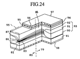
- FIG. 24 is a perspective sectional view showing a Fabry-Pérot semiconductor laser according to an embodiment of the present invention.
- This semiconductor laser has a construction such that a gain peak appears in a 1.3 ⁇ m band, and the construction will be described along the manufacturing process.
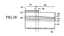
- a first mask 84 having an opening over at least a gain region 79 and a mode conversion regic 80 is formed on an n-type (n - ) InP substrate 81.
- the mask 84 is obtained by patterning an insulating film such as a silicon nitride film by photolithography, and the configuration of the opening 85 of the mask 84 has a rectangular portion 85a having a length of 400 ⁇ m measured in a light travelling direction in thegain region 79, a trapezium portion 85b having a length of 350 ⁇ m and a width Which increases uniformly at a constant angle with greater distance from the base of the rectangular portion 85a, and an extended portion 85cextending further from the base of the trapezium portion 85b.
- an n-InP cladding layer 82, a first SCH layer 83 composed of In x Ga 1-x As y P 1-y (0 ⁇ x ⁇ 1, 0 ⁇ y ⁇ 1), an MQW layer 86, a second SCH layer 87 composed of In x Ga 1- - x As y P 1-y , and a p-InP cladding layer 88 are grown, one after another, epitaxially on an n-type InP substrate 81 exposed from the first mask 84.
- the n-InP cladding layer 82 is grown to a thickness of 100 nm
- the first and the second SCH layers 83 and 87 are grown to a thickness of 100 nm
- the p-InP cladding layer 88 is grown to a thickness of 200 nm.
- Crystals of these layers are not grown on the mask 84 which has no growth nucleus, but are grown selectively on the n-type InP substrate 81 located in the opening portion 85 of the mask 84. Moreover, in these layers, the film thickness is thickest in the stripe-shaped gain region 79 of the opening portion 85 of the mask 84, and the film thickness gets smaller with increasing distance from the gain region 79 in the mode converting region 80 extending therefrom. Such a method of growing a film is called a selective area growth method.
- the thickness of well layers 86a of the MQW layer 86 at the bottom end portion of the mode converting region 80 is 1/3 of the film thickness in the gain region 79.
- This MQW layer 86 functions as an active layer in the gain region 79, and serves as a waveguide in the mode converting region 80. Since the MQW layer 86 is formed in a tapered shape in the mode converting region 80, that region may also be referred to as a tapered region hereinafter.
- the MQW layer 86 is made up of three well layers 86a composed of In x Ga 1-x , As y , P 1-y , (0 ⁇ x' ⁇ 1, 0 ⁇ y' ⁇ 1) and barrier layers 86b composed of In x ,, Ga 1- - x ,,As y ,, P 1-y ,, (0 ⁇ x" ⁇ 1, 0 ⁇ y” ⁇ 1) sandwiched therebetween, and the thickness of the well layer 86a is 7 nm and the thickness of the barrier layer 86b is 15 nm in the gain region 79, respectively.
- a second mask 89 is formed on the p-InP cladding layer 88 and extends in the light travelling direction as shown in FIG. 27A which is a sectional view taken along a line IV-IV in FIG. 25B.
- the mask 89 is obtained by applying patterning to a silicon nitride film thereby to form it in a rectangular stripe shape 1.5 ⁇ m in width.
- the beam spot is formed in a circular or nearly circular shape with the ratio of the minimum values of the stripe widths in the gain region 79 and the mode converting region 80 set to 0.8 to 1.2.
- the p-InP cladding layer 88 to the upper part of the n-InP cladding layer 82 are shaped by etching in an almost perpendicular direction using the second mask 89 as shown in FIG. 27B. Then, a first p-InP buried layer 90 and an n-InP buried layer 91 are formed one after another on the n-InP cladding layer 82 located on both sides of the second mask 89 as shown in FIG. 27C, without removing the second mask 89.
- p-InP is laminated on the p-InP cladding layer 88 and the n-InP buried layer 91, thereby to increase the thickness of the second cladding layer 88 and also to form a second p-InP buried layer 92 on the n-InP buried layer 91 so as to form a current blocking layer 93 (see Figure 24) having a thyristor construction on both sides of the MQW layer 86.
- p+ type InGaAsP is laminated on p-InP as shown in FIG. 26B, which is used as a contact layer 94. This contact layer 94 is made not to cover the tapered region 80 either by using a mask for preventing crystal growth or by applying patterning to the semiconductor layer.
- an insulating film 95 is formed on the contact layer 94, the buried layer 92 and the second cladding layer 88, and an opening portion 96 is formed only above the MQW layer 86 of the gain region 79 by applying patterning to the insulating film 95 by photolithography.
- a p-side electrode 97 is formed on the contact layer 94 and an n-side electrode 98 is formed on the under surface of the n-InP substrate 81 as shown in FIG. 26C. Furthermore, both side faces of the InP substrate 81 and the semiconductor layers formed on the substrate 81 are cleaved. Besides, a reflecting film may also be formed on the cleaved surface of the gain region 79.
- FIG. 24 shows a partly-cut-away perspective view of a Fabry-Perot semiconductor laser formed by the process as described above. Since the taper configuration in the mode converting region 80 of the MQW layer of this semiconductor laser is obtained by defining the shape of the mask, which is used for growing a film, without changing the etching process, crystal defects are less likely to be produced in the tapered part of the MQW layer. As a result, adverse effects on the characteristics due to crystal defects are not produced in this layer. Moreover, the taper configuration is formed with small error and high yield, thus making it possible to obtain beam spots having a uniform configuration.
- the light which has oscillated in the gain region 79 resonates with the reflection from the end face of the gain region 79 and the end face of the mode converting region 80 and is outputted from the end face on the side of the mode converting region 80.
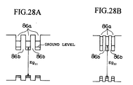
- the potential at the ground level of the quantum well becomes larger as a well layer 86a gets thinner owing to a quantum size effect, and the band gap between the conductive band and the valence band of the well is also expanded. Since a band gap Eg 11 in the gain region 79 shown in FIG. 28A is smaller than a band gap Eg 22 in the mode converting region 80 shown in FIG. 28B, the MQW layer 86 in the mode converting region 80 transmits the light oscillated in the gain
- the variation of the film thickness of the MQW layer 86 in the tapered region 80 is gentle, however, a part of the tapered MQW layer 86 that is near the gain region 79 may become a saturable absorption layer.
- a saturable absorption layer is in existence, the light is absorbed until the layer is saturated by the carriers. Therefore, the threshold gets higher and a kink is produced in the optical output vs. current characteristic (I-L characteristic) curve, thus making sufficient light intensity no longer obtainable.
- the structure such that the p-side electrode 97 and the contact layer 94 in the gain region 79 of the semiconductor laser extended to a saturable absorption region 78 in the vicinity of the tapered region 80, and a current is also injected into the MQW layer 86 of the saturable absorption region 78.
- a current is also injected to the MQW layer 86 of the saturable absorption region 78 through the electrode 97, and light absorption in that region of the MQW layer 86 is countered by injection of carriers, so that the layer 86 does not become a saturable absorption layer, but becomes transparent and transmits the light.
- a kink is no longer produced in the I-L characteristic curve, thus obtaining a characteristic such as shown in FIG. 30.
- wavelength characteristic is shifted toward the short side of the oscillation wavelength (the side having lower wavelengths than the oscillation wavelength) and almost no saturable absorption region is generated in the mode converting region 80, neither hysteresis nor kinks are generated along the L-I curve, and it has been confirmed that reflection or radiation of light at the junction portion of the active region 79 and the tapered region 80 in the MQW layer 86 is controlled to be sufficiently low.
- the full width at half maximum (FWHM) of an output beam is 11.8° in the film thickness (vertical) direction and 8.0° in the lateral (horizontal) direction of the film as shown in FIGs. 31A and 31B, thus obtaining a beam output angle narrower than before.
- the thickness of the well layer 86a of the MQW layer 86 in the tapered region 80 was set to 1/5 of the thickness of the well layer 86a in the gain region 79.
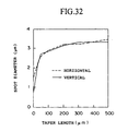
- the mode of the light cannot follow the change of the film thickness and adequate functioning as a mode converter is not obtainable when the length is such that the film thickness changes suddenly, i.e., the taper length is 50 ⁇ m or less.
- changes in film thickness which are suitable for proper functioning as a mode converter can be provided when the taper length is 50 ⁇ m or more even if the change of the spot diameter is gentle.
- no change is noticed in the spot diameter when the taper length reaches 500 ⁇ m or more, and lengths longer than 500 ⁇ m therefore are unnecessary.
- the optimum taper length is 50 ⁇ m or more and preferably 50 to 500 ⁇ m.
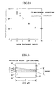
- FIG. 33 shows a result of calculating how the beam output angle from the output end is changed when the film thickness ratio between the input end and the output end (input end film thickness/output end film thickness) of the mode converting region 80 of the MQW layer 86 that becomes the tapered waveguide is changed from 1 to 5.
- a normal three-dimensional beam propagation method is used for computation, which has been made on an MQW waveguide of a 1.3 ⁇ m band.
- the film thickness of the MQW layer 86 at the input end is set to 0.1 ⁇ m
- the thickness of the SCH layers 83 and 87 is set to 0.1 ⁇ m
- the length l of the waveguide is set to 200 ⁇ m
- a loss-less waveguide in which change of the film thickness is uniform has been assumed.
- the lateral width of the tapered waveguide was set constant at 1 ⁇ m over the whole length of the waveguide.
- a square dot shows an emission angle of a beam in a horizontal direction with respect to the substrate surface
- a rhombic dot shows an emission angle of a beam in a vertical direction with respect to the substrate surface.
- the emission angle is narrowed as the film thickness ratio becomes larger, and the angle reaches 15 degrees and 12 degrees when the film thickness ratio is 3 and 4, respectively. Further, the fact that the values of emission angles in the horizontal direction and the vertical direction for the same ratio become closer to one another as the ratio increases shows that the beam configuration becomes nearly circular, and a desirable result for the coupling with an optical fiber is obtained as the beam configuration gets nearer to a circle.
- the film thickness ratio of the MQW layer 86 is preferably 3 or higher.
- the film thickness ratio is 2
- an improvement can be expected in the coupling efficiency owing to the fact that the beam gets nearer to a circle than a conventional laser and the mode configuration of the laser becomes close to the mode configuration of the optical fiber.
- the MQW layer of the optical modulation region may be made of a composition having a shorter wavelength as compared with the composition of the MQW layer of the gain region.
- the composition formed in the optical modulation region may be of wavelength 1.20 ⁇ m to 1.22 ⁇ m.
- the composition in the optical modulation region may be of wavelength approximately 1.40 ⁇ m to 1.45 ⁇ m.
- the film thickness ratio falls within the range of 1.5 to 2.
- the composition is formed to have a film thickness ratio larger than the above, sufficient light absorption becomes unachievable unless the voltage for optical modulation is increased since the composition wavelength in the optical modulation region is too high. As a result, the working voltage of elements has to be raised.
- the film thickness of the MQW layer in the gain region of the integrated light source and optical modulator described in those patent provisional publications is up to two times the film thickness of the MQW layer of the optical modulation region.
- the change of the film thickness of the MQW layer is smaller, and it thus differs from an effective change quantity of the film thickness of a semiconductor laser having an integrated mode converter embodying the present invention.
- the effective ranges of the change of the film thickness are different as between an optical modulator integrated light source and an optical mode converter integrated light source, and, in a light source having an integrated mode converter, it is required to make the film thickness of the waveguide layer of the mode converter two times or more at the input end against the output end, and a circular beam is obtainable by making the film thickness ratio five times.
- the change of the film thickness does not need to be uniform, and the film thickness may change suddenly in the vicinity of the gain region 79 and change gently with greater distance therefrom, or conversely may change gently in the vicinity of the gain region 79, or the rate of change of the film thickness may be changed gently a plurality of times. Further, the film thickness thereof may also be changed gently stepwise.
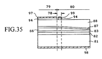
- two p-side electrodes 97 and 99 may be formed separately in the gain region 79 and the saturable absorption region 78 respectively as shown in FIG. 35. With this, a current injection quantity in the saturable absorption region 78 becomes less and power consumption is reduced.
- the contact layer 94 composed of an impurity-containing semiconductor has a higher resistance than a p-side electrode 97 made of metal, and a current injected into the MQW layer 86 through the contact layer 94 gets smaller with increasing distance from the gain region 79. Hence, it is possible to control supply of an excessive current.
- a Fabry-Perot construction has been adopted in the present embodiment, but a DBR laser construction may also be adopted by providing a diffraction grating above or below the MQW layer 86 of the mode converting region 80. Further, a diffraction grating may be provided along the MQW layer of the gain region so as to obtain a DFB laser construction.
- the MQW layer is structured with InGaAsP/InP or InGaAs/InP group materials in the above mentioned embodiment, but an MQW formed of an GaAs/AlGaAs or AlGaAs/AlGaAs group material, an GaInP/AlGaInP or AlGaInP/AlGaInP group material or other compound semiconductor materials may also be used.
- the growth of the compound semiconductor layer may be performed by MOCVD, MBE or other epitaxial growth methods.
Landscapes
- Physics & Mathematics (AREA)
- General Physics & Mathematics (AREA)
- Optics & Photonics (AREA)
- Condensed Matter Physics & Semiconductors (AREA)
- Electromagnetism (AREA)
- Engineering & Computer Science (AREA)
- Microelectronics & Electronic Packaging (AREA)
- Semiconductor Lasers (AREA)
- Optical Integrated Circuits (AREA)
Claims (36)
- Un dispositif optique à semiconducteur dans lequel un élément optique actif (35; 57; 70) et un guide d'ondes (36; 58; 69A; 69B) sont formés de manière intégrée, le dispositif comprenant :caractérisé en ce que l'épaisseur de la couche de puits (20a; 86a) diminue progressivement sur la longueur de la région de guide d'ondes (17; 80) à partir de sa première extrémité jusqu'à sa seconde extrémité.une structure de support (11, 13-15; 81-83) ayant un substrat semiconducteur (11; 81); etune structure de puits quantiques (20; 86) formée sur la structure de support et ayant une pile de couches comprenant au moins une couche de puits (20a, 86a) et deux couches de barrière (20b; 86b) entre lesquelles la couche de puits (20a; 86a) est intercalée, la structure de puits quantiques étant formée dans une région optique active (12; 79) de l'élément optique actif (35; 57; 70), et étant également formée dans une région de guide d'ondes (17; 80) qui a une première extrémité adjacente à la région optique active (12; 79) et qui a une seconde extrémité adjacente à une partie d'interface du dispositif, à laquelle un faisceau optique de sortie est émis par le dispositif, ou un faisceau optique d'entrée est reçu par le dispositif, lorsque le dispositif est en cours d'utilisation, la structure de puits quantiques (20; 86) dans la région de guide d'ondes (17; 80) formant au moins une partie d'une couche de coeur (20; 86) du guide d'ondes (36; 58; 69A, 69B) et ayant pour fonction de coupler optiquement l'élément optique actif (35; 57; 70) à la partie d'interface lorsque le dispositif est en cours d'utilisation, des couches de gaine supérieure et inférieure (15, 22/28; 82, 88) étant formées respectivement au-dessus et au-dessous de la couche de coeur (20; 86);
- Un dispositif selon la revendication 1, dans lequel la structure de puits quantiques (20; 86) comprend un ensemble de telles couches de puits (20a; 86a) et un ensemble de telles couches de barrière (20b; 86b), les couches de puits (20a; 86b) et les couches de barrière (20b; 86b) étant empilées les unes sur les autres de manière alternée.
- Un dispositif selon la revendication 1 ou 2, dans lequel les couches de barrière (20b; 86b) ont une épaisseur qui diminue progressivement à partir de la première extrémité jusqu'à la seconde extrémité de la région de guide d'ondes (17; 80).
- Un dispositif selon l'une quelconque des revendications précédentes, dans lequel dans la région de guides d'ondes (17; 80) la structure de puits quantiques (20; 86) a une largeur qui augmente progressivement à partir de la première extrémité jusqu'à la seconde extrémité.
- Un dispositif selon l'une quelconque des revendications 1 à 3, dans lequel la structure de puits quantiques (86) a pratiquement une forme de ruban au-dessus de la région optique active (79) et au-dessus de la région de guide d'ondes (80), et le rapport entre la valeur de largeur minimale de la structure de puits quantiques au-dessus de la région optique active (79) et la valeur de largeur minimale de la structure de puits quantiques au-dessus de la région de guide d'ondes (80) est dans la plage de 0,8 à 1,2.
- Un dispositif selon l'une quelconque des revendications précédentes, dans lequel l'épaisseur totale de la structure de puits quantiques (20; 86) à la première extrémité est au moins le double de celle à la seconde extrémité.
- Un dispositif selon l'une quelconque des revendications précédentes, comprenant en outre :une première couche de guide (19; 83) formée entre la structure de puits quantiques (20; 86) et la couche de gaine inférieure (15; 82); etune seconde couche de guide (21; 87) formée entre la structure de puits quantiques (20; 86) et la couche de gaine supérieure (22; 88);les première et seconde couches de guide (19, 21; 83, 87) ayant une bande d'énergie interdite qui est supérieure à celle de la structure de puits quantiques (20; 86) et inférieure aux bandes interdites respectives des couches de gaine supérieure et inférieure (15, 22; 82, 88).
- Un dispositif selon la revendication 7, dans lequel les première et seconde couches de guide (19, 21) ont une épaisseur qui se réduit progressivement, dans leurs parties qui s'étendent au-dessus ou au-dessous de la région de guide d'ondes (17) de la structure de puits quantiques, dans la direction allant de la première extrémité vers la seconde extrémité.
- Un dispositif selon l'une quelconque des revendications précédentes, dans lequel un réseau de diffraction (13) pour former un élément réfléchissant de rétroaction répartie est en outre formé sous la région optique active (12; 79) de la structure de puits quantiques (20; 86).
- Un dispositif selon l'une quelconque des revendications précédentes, dans lequel la couche de gaine supérieure (22, 28) s'étend au-dessus de la région optique active (12) ainsi qu'au-dessus de la région de guide d'ondes (17; 80) de la structure de puits quantiques, et elle comporte un sillon (32) pour séparer cette couche en deux parties, l'une de ces parties s'étendant au-dessus de la région optique active (20a) et l'autre partie s'étendant au-dessus de la région de guide d'ondes (20b).
- Un dispositif selon la revendication 10, dans lequel le sillon (32) dans la couche de gaine supérieure (22, 28) est rempli avec un matériau isolant (38).
- Un dispositif selon l'une quelconque des revendications précédentes, comportant une première électrode (33, 98) formée sur une face principale inférieure du substrat (11; 81) et comportant également une seconde électrode (34; 97), formée au-dessus de la couche de gaine supérieure (22, 28; 88), et s'étendant au moins au-dessus de la région optique active (12; 79) de la structure de puits quantiques.
- Un dispositif selon la revendication 12, comprenant en outre une couche de contact (94) formée entre la seconde électrode (97) et la couche de gaine supérieure (88).
- Un dispositif selon la revendication 13, dans lequel la couche de contact (94) s'étend au-delà de la région optique active (79), de façon à être présente également au-dessus d'une partie (78) de la région de guide d'ondes (80).
- Un dispositif selon la revendication 14, dans lequel la seconde électrode (97) s'étend également au-delà de la région optique active (79) de façon à être présente au-dessus de la partie précitée (78) de la région de guide d'ondes (80).
- Un dispositif selon la revendication 13, dans lequel la seconde électrode (97) et la couche de contact (94) sont toutes deux séparées, en coïncidence l'une avec l'autre, en deux parties à l'endroit auquel elles s'étendent au-dessus d'une région frontière entre la région optique active (79) et la région de guide d'ondes (80).
- Un dispositif selon la revendication 7, dans lequel la couche de puits (20a; 86a), ou chacune d'elles, consiste en InGaAs ou InGaAsP, les couches de barrière (20b; 86b) consistent en InGaAsP, les première et seconde couches de guide (19, 21; 83, 87) consistent en InGaAsP, et le substrat semiconducteur (11; 81) et les couches de gaine supérieure et inférieure (15, 22/28; 82, 88) consistent en InP.
- Un dispositif selon l'une quelconque des revendications 1 à 17, dans lequel la couche de puits (86a), ou chacune d'elles, consiste en InGaAsP ayant un premier rapport de composition, et les couches de barrière (86b) consistent en InGaAsP ayant un second rapport de composition qui est différent du premier rapport de composition.
- Un dispositif selon l'une quelconque des revendications 1 à 16, dans lequel la couche de puits (86a), ou chacune d'elles, consiste en GaAs, et les couches de barrière (86b) consistent en AlGaAs.
- Un dispositif selon l'une quelconque des revendications 1 à 16, dans lequel la couche de puits (86a), ou chacune d'elles, consiste en GalnP, et les couches de barrière (86b) consistent en AlGalnP.
- Un dispositif selon l'une quelconque des revendications précédentes, comprenant des couches enterrées (25; 93) formées des deux côtés de la couche de puits quantiques (20; 86).
- Un dispositif selon l'une quelconque des revendications précédentes, dans lequel une face principale inférieure de la structure de puits quantiques (20; 86) s'étend de façon pratiquement parallèle à une face supérieure principale du substrat semiconducteur (11; 81).
- Un dispositif selon l'une quelconque des revendications précédentes, dans lequel l'élément optique actif est un laser à semiconducteur (35), un amplificateur à laser à semiconducteur (70), une diode électroluminescente du type à émission de lumière par la face d'extrémité, une photodiode du type à guide d'ondes (57) ou un modulateur optique à semiconducteur.
- Un dispositif selon l'une quelconque des revendications précédentes, dans lequel les couches de gaine supérieure et inférieure (15, 22) sont constituées par un matériau semiconducteur qui n'est pas dopé avec des impuretés.
- Un procédé de fabrication d'un dispositif optique à semiconducteur dans lequel un élément optique actif (35; 57; 70) et un guide d'ondes (36; 58; 69A, 69B) sont formés de manière intégrée, comprenant les étapes suivantes :on forme une pellicule de masquage (16; 84) en un matériau diélectrique sur une face principale supérieure d'une structure de support (11, 13-15; 81) comprenant un substrat semiconducteur (11; 81);on définit un motif dans la pellicule de masquage (16; 84) de façon à mettre à nu des première (12; 85a) et seconde (17; 85b) régions respectives de matériau semiconducteur (15; 81) de la structure de support, la première région (12; 85a) correspondant à une région optique active (12; 79) de l'élément optique actif (36; 58; 69A; 69B) et étant allongée, et la seconde région (17; 85b) correspondant à une région de guide d'ondes (17; 80) et ayant une largeur qui augmente progressivement à partir de sa première extrémité adjacente à une extrémité de la première région (12; 85a), jusqu'à sa seconde extrémité adjacente à une partie d'interface désirée du dispositif fini à laquelle, au cours de l'utilisation de ce dispositif fini, un faisceau optique de sortie doit être émis par le dispositif, ou un faisceau optique d'entrée doit être reçu par le dispositif; eton forme successivement des couches (19 à 23; 86 à 88) au-dessus des première et seconde régions (12, 17; 85a, 85b), de façon à former au-dessus des deux régions une structure de puits quantiques (20; 86) ayant un empilement des couches comprenant au moins une couche de puits (20a; 86a) et deux couches de barrière (20b; 86b) entre lesquelles la couche de puits (20a; 86a) est intercalée, la structure de puits quantiques (20; 86) au-dessus de la seconde région formant au moins une partie d'une couche de coeur du guide d'ondes (36; 58; 69A; 69B), et de façon à former au moins au-dessus de la seconde région (17; 85b) des couches de gaine supérieure et inférieure (15, 22/28; 82, 88), respectivement au-dessus et au-dessous de la structure de puits quantiques (20; 86), la couche de puits (20a; 86a), au moins, étant formée par un procédé de croissance à sélectivité de zone, de façon que son épaisseur diminue progressivement sur la longueur de la seconde région, à partir de sa première extrémité jusqu'à sa seconde extrémité.
- Un procédé selon la revendication 25, dans lequel la couche de puits (20a; 86a), ou chacune d'elles, et chaque couche de barrière (20b; 86b) sont formées par le procédé de croissance à sélectivité de zone, de façon que l'épaisseur des couches de puits comme des couches de barrière diminue progressivement sur la longueur de la seconde région.
- Un procédé selon la revendication 25 ou 26, dans lequel la seconde région (17; 85b) a une forme pratiquement semblable à un trapèze dont les deux côtés parallèles se trouvent respectivement aux première et seconde extrémités de la seconde région (17; 85b).
- Un procédé selon la revendication 27, dans lequel la largeur du trapèze, mesurée entre ses deux côtés non parallèles, change pas à pas à partir de la première extrémité jusqu'à la seconde extrémité.
- Un procédé selon l'une quelconque des revendications 25 à 28, dans lequel le matériau semiconducteur (15) de la structure de support (11; 13-15; 81-83) remplit la fonction de la couche de gaine inférieure dans le dispositif fini.
- Un procédé selon l'une quelconque des revendications 25 à 29, dans lequel le matériau semiconducteur de la structure de support est constitué par une couche de semiconducteur (15) qui est formée au-dessus du substrat semiconducteur (11), et les première et seconde régions de matériau semiconducteur qui sont mises à nu dans l'étape de définition d'un motif dans la pellicule de masquage font partie de cette couche de semiconducteur (15).
- Un procédé selon l'une quelconque des revendications 25 à 29, dans lequel les première et seconde régions de matériau semiconducteur qui sont mises à nu dans l'étape de définition d'un motif dans la pellicule de masquage font partie du substrat semiconducteur (81).
- Un procédé selon l'une quelconque des revendications 25 à 31, dans lequel l'étape de formation de couches comprend les étapes suivantes :on forme une première telle couche de barrière (20b; 86b) au-dessus des première et seconde régions de la couche de semiconducteur (15; 83);on forme une telle couche de puits (20a; 86a) sur la première couche de barrière (20b; 86b); eton forme une seconde telle couche de barrière (20b; 86b) sur la couche de puits (20a; 86a).
- Un procédé selon l'une quelconque des revendications 25 à 32, comprenant en outre les étapes suivantes :on enlève la pellicule de masquage (16; 84) de la structure de support;on forme une première électrode (33; 98) sous la structure de support (11, 13-15; 81-83); eton forme une seconde électrode (34; 97) au-dessous de la couche de gaine supérieure (28; 88) de façon que l'électrode s'étende au-dessus de la première région (12; 85a).
- Un procédé selon la revendication 33, comprenant en outre une étape de formation d'une couche de contact (94) entre la couche de gaine supérieure (88) et la seconde électrode (97).
- Un procédé selon l'une quelconque des revendications 25 à 34, comprenant en outre une étape, après l'étape de formation de couches, qui consiste à définir un motif dans les couches formées (19-23) pour leur donner une forme de ruban à l'endroit auquel elles s'étendent au-dessus de la première région (12), avant l'achèvement de la couche de gaine supérieure (28).
- Un procédé selon l'une quelconque des revendications 25 à 34, comprenant en outre une étape, après l'étape de formation de couches, consistant à définir un motif dans les couches formées (86-88), pour leur donner une forme de ruban à l'endroit auquel elles s'étendent à la fois au-dessus des première et seconde régions (85a, 85b).
Applications Claiming Priority (6)
| Application Number | Priority Date | Filing Date | Title |
|---|---|---|---|
| JP216006/93 | 1993-08-31 | ||
| JP21600693A JPH0766502A (ja) | 1993-08-31 | 1993-08-31 | 光半導体装置及びその形成方法 |
| JP18721/94 | 1994-02-15 | ||
| JP1872194 | 1994-02-15 | ||
| JP16514594A JP3548986B2 (ja) | 1994-02-15 | 1994-07-18 | 光半導体装置及びその製造方法 |
| JP165145/94 | 1994-07-18 |
Publications (2)
| Publication Number | Publication Date |
|---|---|
| EP0641049A1 EP0641049A1 (fr) | 1995-03-01 |
| EP0641049B1 true EP0641049B1 (fr) | 1998-10-28 |
Family
ID=27282337
Family Applications (1)
| Application Number | Title | Priority Date | Filing Date |
|---|---|---|---|
| EP94306456A Expired - Lifetime EP0641049B1 (fr) | 1993-08-31 | 1994-08-31 | Dispositif optique à semi-conducteur et sa méthode de fabrication |
Country Status (3)
| Country | Link |
|---|---|
| US (2) | US5987046A (fr) |
| EP (1) | EP0641049B1 (fr) |
| DE (1) | DE69414208T2 (fr) |
Families Citing this family (73)
| Publication number | Priority date | Publication date | Assignee | Title |
|---|---|---|---|---|
| JPH08307012A (ja) * | 1995-05-01 | 1996-11-22 | Mitsubishi Electric Corp | 選択成長用マスク,半導体光装置の製造方法,および半導体光装置 |
| JPH09153638A (ja) * | 1995-11-30 | 1997-06-10 | Nec Corp | 導波路型半導体受光装置およびその製造方法 |
| DE19626130A1 (de) * | 1996-06-28 | 1998-01-08 | Sel Alcatel Ag | Optisches Halbleiterbauelement mit tiefem Rippenwellenleiter |
| DE19626113A1 (de) * | 1996-06-28 | 1998-01-02 | Sel Alcatel Ag | Optisches Halbleiterbauelement mit tiefem Rippenwellenleiter |
| CA2218262C (fr) * | 1996-10-17 | 2001-04-24 | Kenji Kawano | Modulateur optique ultrarapide a semi-conducteur comportant une electrode a ondes progressives |
| JP3758258B2 (ja) * | 1996-11-29 | 2006-03-22 | 富士通株式会社 | 光結合装置 |
| JP2967737B2 (ja) * | 1996-12-05 | 1999-10-25 | 日本電気株式会社 | 光半導体装置とその製造方法 |
| DE19712620A1 (de) * | 1997-03-26 | 1998-10-01 | Univ Schiller Jena | Laserdiode mit geringem Abstrahlwinkel in der Form eines Streifenwellenleiters und Verfahren zu ihrer Herstellung |
| JP3104789B2 (ja) | 1997-05-02 | 2000-10-30 | 日本電気株式会社 | 半導体光素子およびその製造方法 |
| JPH11103130A (ja) * | 1997-09-29 | 1999-04-13 | Mitsubishi Electric Corp | 半導体光素子,及びその製造方法 |
| US6034380A (en) * | 1997-10-07 | 2000-03-07 | Sarnoff Corporation | Electroluminescent diode with mode expander |
| US6052397A (en) * | 1997-12-05 | 2000-04-18 | Sdl, Inc. | Laser diode device having a substantially circular light output beam and a method of forming a tapered section in a semiconductor device to provide for a reproducible mode profile of the output beam |
| JP3682367B2 (ja) * | 1998-01-28 | 2005-08-10 | パイオニア株式会社 | 分布帰還型半導体レーザ |
| JP3792040B2 (ja) * | 1998-03-06 | 2006-06-28 | 松下電器産業株式会社 | 双方向光半導体装置 |
| JP2000066046A (ja) | 1998-08-21 | 2000-03-03 | Hitachi Ltd | 光伝送装置 |
| JP4570712B2 (ja) * | 1999-10-14 | 2010-10-27 | Okiセミコンダクタ株式会社 | 半導体導波路素子及びその製造方法 |
| KR100406865B1 (ko) * | 1999-11-04 | 2003-11-21 | 삼성전자주식회사 | 선택 영역 성장법을 이용한 2중 코아 스폿 사이즈 변환기및 그 제조방법 |
| TW479387B (en) * | 1999-11-23 | 2002-03-11 | Nanovation Tech Inc | Optical waveguide having a weakly-confining waveguide section and a strongly-confining waveguide section ooptically coupled by a tapered neck |
| KR20020081237A (ko) * | 1999-12-27 | 2002-10-26 | 코닝 오.티.아이. 에스피에이 | 발산영역을 가진 반도체 레이저 엘리먼트 |
| US6678479B1 (en) * | 2000-03-01 | 2004-01-13 | Opnext Japan, Inc. | Semiconductor electro-absorption optical modulator integrated light emission element light emission element module and optical transmission system |
| JP4471522B2 (ja) * | 2000-03-15 | 2010-06-02 | 浜松ホトニクス株式会社 | 集光部品並びにこれを用いた光源モジュール、レーザー装置及び光信号増幅装置 |
| US6317445B1 (en) * | 2000-04-11 | 2001-11-13 | The Board Of Trustees Of The University Of Illinois | Flared and tapered rib waveguide semiconductor laser and method for making same |
| US6376272B1 (en) * | 2000-06-06 | 2002-04-23 | Lucent Technologies, Inc. | InA1As etch stop layer for precise semiconductor waveguide fabrication |
| US6597718B2 (en) * | 2000-07-18 | 2003-07-22 | Multiplex, Inc. | Electroabsorption-modulated fabry perot laser |
| US7031612B2 (en) | 2000-07-18 | 2006-04-18 | Multiplex, Inc. | Optical transponders and transceivers |
| JP4618854B2 (ja) * | 2000-08-11 | 2011-01-26 | Okiセミコンダクタ株式会社 | 半導体装置およびその製造方法 |
| JP3766953B2 (ja) * | 2000-09-13 | 2006-04-19 | 日本電信電話株式会社 | 光回路 |
| KR100358133B1 (ko) * | 2000-12-30 | 2002-10-25 | 한국전자통신연구원 | 스트레인 분산 패드를 이용한 측면-테이퍼 도파로 제조방법과 이를 응용한 모드변환기 제조방법 및 그에 따른광소자 |
| US20050040386A1 (en) * | 2001-02-20 | 2005-02-24 | Fow-Sen Choa | Multiple quantum well broad spectrum gain medium and method for forming same |
| US6580740B2 (en) * | 2001-07-18 | 2003-06-17 | The Furukawa Electric Co., Ltd. | Semiconductor laser device having selective absorption qualities |
| US6680961B2 (en) * | 2001-08-01 | 2004-01-20 | Binoptics, Inc. | Curved waveguide ring laser |
| GB0127573D0 (en) * | 2001-11-17 | 2002-01-09 | Corning Inc | Semiconductor optical devices and methods of making them |
| US6881983B2 (en) * | 2002-02-25 | 2005-04-19 | Kopin Corporation | Efficient light emitting diodes and lasers |
| JP3666463B2 (ja) * | 2002-03-13 | 2005-06-29 | 日本電気株式会社 | 光導波路デバイスおよび光導波路デバイスの製造方法 |
| US6649990B2 (en) * | 2002-03-29 | 2003-11-18 | Intel Corporation | Method and apparatus for incorporating a low contrast interface and a high contrast interface into an optical device |
| US6989284B2 (en) * | 2002-05-31 | 2006-01-24 | Intel Corporation | Fabrication of a waveguide taper through ion implantation |
| US6956983B2 (en) * | 2002-05-31 | 2005-10-18 | Intel Corporation | Epitaxial growth for waveguide tapering |
| FR2854469B1 (fr) * | 2003-04-01 | 2005-08-05 | Cit Alcatel | Procede de fabrication d'un dispositif optique semi-conducteur comportant une region munie d'une couche active a epaisseur variable |
| US20050008316A1 (en) * | 2003-05-02 | 2005-01-13 | Aydin Yeniay | Optical waveguide amplifier |
| US7122841B2 (en) * | 2003-06-04 | 2006-10-17 | Kopin Corporation | Bonding pad for gallium nitride-based light-emitting devices |
| US20050179042A1 (en) * | 2004-02-13 | 2005-08-18 | Kopin Corporation | Monolithic integration and enhanced light extraction in gallium nitride-based light-emitting devices |
| US20050179046A1 (en) * | 2004-02-13 | 2005-08-18 | Kopin Corporation | P-type electrodes in gallium nitride-based light-emitting devices |
| DE602005024674D1 (de) * | 2004-04-15 | 2010-12-23 | Binoptics Corp | Photonische integrierte bauelemente mit mehreren ebenen |
| FR2879841B1 (fr) * | 2004-12-22 | 2008-10-24 | Thales Sa | Laser semiconducteur de puissance a faibles divergence et astigmatisme |
| KR100738530B1 (ko) * | 2005-07-21 | 2007-07-11 | 삼성전자주식회사 | 광 모드 변환기를 구비한 반도체 레이저 및 그 제조방법 |
| KR100759805B1 (ko) * | 2005-12-07 | 2007-09-20 | 한국전자통신연구원 | 광증폭 듀플렉서 |
| JP4952376B2 (ja) * | 2006-08-10 | 2012-06-13 | 三菱電機株式会社 | 光導波路と半導体光集積素子の製造方法 |
| JP2009033009A (ja) * | 2007-07-30 | 2009-02-12 | Panasonic Corp | 半導体レーザ装置及びその製造方法 |
| US8213751B1 (en) * | 2008-11-26 | 2012-07-03 | Optonet Inc. | Electronic-integration compatible photonic integrated circuit and method for fabricating electronic-integration compatible photonic integrated circuit |
| US8588039B1 (en) | 2011-03-02 | 2013-11-19 | Western Digital (Fremont), Llc | Energy-assisted magnetic recording head having multiple cores of different lengths |
| JP2013016648A (ja) * | 2011-07-04 | 2013-01-24 | Sumitomo Electric Ind Ltd | 半導体光集積素子の製造方法 |
| US9977188B2 (en) * | 2011-08-30 | 2018-05-22 | Skorpios Technologies, Inc. | Integrated photonics mode expander |
| CN102565940A (zh) * | 2012-03-13 | 2012-07-11 | 中国科学院苏州纳米技术与纳米仿生研究所 | 一种三维波导结构及其制作方法 |
| US8509037B1 (en) | 2012-04-24 | 2013-08-13 | Seagate Technology Llc | Layered optical waveguide and near field transducer |
| US8873349B2 (en) | 2012-04-24 | 2014-10-28 | Seagate Technology Llc | Optical devices including assistant layers |
| US8681595B1 (en) | 2013-03-12 | 2014-03-25 | Seagate Technology Llc | Layered optical waveguide and near field transducer |
| US9099138B2 (en) | 2013-12-20 | 2015-08-04 | Seagate Technology Llc | Optical devices including layers that wrap the near field transducer (NFT) |
| WO2015104836A1 (fr) | 2014-01-10 | 2015-07-16 | 富士通株式会社 | Élément semi-conducteur optique et son procédé de fabrication |
| US9664855B2 (en) | 2014-03-07 | 2017-05-30 | Skorpios Technologies, Inc. | Wide shoulder, high order mode filter for thick-silicon waveguides |
| US9658401B2 (en) | 2014-05-27 | 2017-05-23 | Skorpios Technologies, Inc. | Waveguide mode expander having an amorphous-silicon shoulder |
| US10106889B2 (en) | 2014-11-11 | 2018-10-23 | Seagate Technology Llc | Waveguides including novel core materials |
| FR3046850B1 (fr) | 2016-01-15 | 2018-01-26 | Universite De Strasbourg | Guide optique ameliore et systeme optique comportant un tel guide optique |
| WO2018100634A1 (fr) * | 2016-11-29 | 2018-06-07 | 三菱電機株式会社 | Dispositif optique |
| TWI609541B (zh) * | 2016-12-12 | 2017-12-21 | 聯亞光電工業股份有限公司 | 半導體雷射裝置 |
| US10649148B2 (en) | 2017-10-25 | 2020-05-12 | Skorpios Technologies, Inc. | Multistage spot size converter in silicon photonics |
| US11245248B2 (en) * | 2018-01-10 | 2022-02-08 | Sony Semiconductor Solutions Corporation | Semiconductor laser |
| CN108963756B (zh) * | 2018-07-02 | 2020-10-16 | 福建中科光芯光电科技有限公司 | 一种光通信波段多波长半导体激光器的制备方法 |
| JP7379334B2 (ja) * | 2018-07-27 | 2023-11-14 | ヌヴォトンテクノロジージャパン株式会社 | 半導体レーザ素子、検査方法及び検査装置 |
| US11360263B2 (en) | 2019-01-31 | 2022-06-14 | Skorpios Technologies. Inc. | Self-aligned spot size converter |
| JP7279658B2 (ja) * | 2020-02-12 | 2023-05-23 | 住友電気工業株式会社 | 半導体光素子およびその製造方法 |
| CN113991421A (zh) * | 2021-10-26 | 2022-01-28 | 中国科学院半导体研究所 | 半导体微腔激光器 |
| EP4311042B1 (fr) * | 2022-07-21 | 2025-10-15 | Nokia Solutions and Networks Oy | Dispositif opto-électronique |
| US12596229B2 (en) * | 2022-08-12 | 2026-04-07 | Purdue Research Foundation | 3D tapered nanophotonic waveguide to fiber edge coupler |
Family Cites Families (19)
| Publication number | Priority date | Publication date | Assignee | Title |
|---|---|---|---|---|
| JPS5898996A (ja) * | 1981-12-03 | 1983-06-13 | ゼロツクス・コ−ポレ−シヨン | 注入形レ−ザ |
| JPH073905B2 (ja) * | 1987-03-23 | 1995-01-18 | 日本電信電話株式会社 | 半導体レ−ザおよびその製造方法 |
| JPS6453487A (en) * | 1987-08-24 | 1989-03-01 | Nec Corp | Semiconductor laser device |
| JPS6473689A (en) * | 1987-09-14 | 1989-03-17 | Sharp Kk | Semiconductor laser device |
| JPH067603B2 (ja) * | 1987-11-16 | 1994-01-26 | 日本電信電話株式会社 | 発光ダイオード |
| US4961198A (en) * | 1988-01-14 | 1990-10-02 | Matsushita Electric Industrial Co., Ltd. | Semiconductor device |
| JPH069280B2 (ja) * | 1988-06-21 | 1994-02-02 | 松下電器産業株式会社 | 半導体レーザ装置 |
| JP2836822B2 (ja) * | 1988-06-23 | 1998-12-14 | 日本電信電話株式会社 | 導波路型半導体光素子の製造方法 |
| US5048907A (en) * | 1990-02-23 | 1991-09-17 | Amoco Corporation | Electric field induced quantum well waveguides |
| JPH03284891A (ja) * | 1990-03-30 | 1991-12-16 | Fujitsu Ltd | 光半導体素子 |
| EP0643461B1 (fr) * | 1990-08-24 | 1997-10-29 | Nec Corporation | Méthode pour la fabrication d'un dispositif optique à semi-conducteur |
| WO1992004753A1 (fr) * | 1990-09-12 | 1992-03-19 | The Furukawa Electric Co., Ltd. | Element laser a semi-conducteur du type a puits quantiques |
| EP0495202B1 (fr) * | 1991-01-15 | 1996-04-24 | Siemens Aktiengesellschaft | Dispositif pour changer une onde optique avec un petit diamètre du mode en une onde avec un diamètre plus grand |
| JPH05249331A (ja) * | 1992-01-09 | 1993-09-28 | Nippon Telegr & Teleph Corp <Ntt> | 導波路形ビームスポット変換素子およびその製造方法 |
| JPH05327111A (ja) * | 1992-05-20 | 1993-12-10 | Fujitsu Ltd | 半導体レーザ装置及びその製造方法 |
| US5323476A (en) * | 1992-08-14 | 1994-06-21 | Siemens Aktiengesellschaft | Apparatus for increasing the cross section of optical waves |
| JP2555954B2 (ja) * | 1993-11-02 | 1996-11-20 | 日本電気株式会社 | 半導体レーザ |
| JPH09153638A (ja) * | 1995-11-30 | 1997-06-10 | Nec Corp | 導波路型半導体受光装置およびその製造方法 |
| US6052397A (en) * | 1997-12-05 | 2000-04-18 | Sdl, Inc. | Laser diode device having a substantially circular light output beam and a method of forming a tapered section in a semiconductor device to provide for a reproducible mode profile of the output beam |
-
1994
- 1994-08-31 EP EP94306456A patent/EP0641049B1/fr not_active Expired - Lifetime
- 1994-08-31 DE DE69414208T patent/DE69414208T2/de not_active Expired - Lifetime
-
1997
- 1997-04-02 US US08/826,533 patent/US5987046A/en not_active Expired - Fee Related
-
1999
- 1999-09-22 US US09/401,784 patent/US6238943B1/en not_active Expired - Fee Related
Also Published As
| Publication number | Publication date |
|---|---|
| US6238943B1 (en) | 2001-05-29 |
| EP0641049A1 (fr) | 1995-03-01 |
| DE69414208D1 (de) | 1998-12-03 |
| US5987046A (en) | 1999-11-16 |
| DE69414208T2 (de) | 1999-03-25 |
Similar Documents
| Publication | Publication Date | Title |
|---|---|---|
| EP0641049B1 (fr) | Dispositif optique à semi-conducteur et sa méthode de fabrication | |
| US5585957A (en) | Method for producing various semiconductor optical devices of differing optical characteristics | |
| US5220573A (en) | Optical apparatus using wavelength selective photocoupler | |
| US7463663B2 (en) | Semiconductor laser diode and integrated semiconductor optical waveguide device | |
| EP0725287B1 (fr) | Elément intégré de contrôle optique et un procédé de fabrication pour celui-ci et élément de circuit intégré optique et dispositif de circuit intégré optique utilisant celui-ci | |
| JPH04254380A (ja) | モノリシック集積光増幅器及び光検出器 | |
| JPH0750443A (ja) | 半導体光集積素子及びその製造方法 | |
| JP4026334B2 (ja) | 半導体レーザ、分布帰還型半導体レーザおよび波長可変半導体レーザ | |
| US5703974A (en) | Semiconductor photonic integrated circuit and fabrication process therefor | |
| US4622674A (en) | Single longitudinal mode semiconductor laser | |
| EP0672932B1 (fr) | Modulateur optique à semi-conducteur | |
| JP3284994B2 (ja) | 半導体光集積素子及びその製造方法 | |
| JPH0766502A (ja) | 光半導体装置及びその形成方法 | |
| JP3421999B2 (ja) | 光機能素子、これを含む光集積素子およびそれらの製造方法 | |
| US4665527A (en) | Distributed feedback semiconductor laser | |
| JPH04783A (ja) | 半導体光素子 | |
| JPH04105383A (ja) | 半導体光集積素子の製造方法 | |
| JP3061169B2 (ja) | 半導体レーザ | |
| CN115280609B (zh) | 光学器件 | |
| US4974233A (en) | Semiconductor laser device | |
| JP3186645B2 (ja) | 半導体レーザ及びその製造方法 | |
| CN120566223B (zh) | 集成分支波导和光电二极管的半导体器件 | |
| JP2001148542A (ja) | 光半導体装置及びその製造方法並びに光通信装置 | |
| KR100228396B1 (ko) | 선택성 식각층을 이용한 고 효율의 광변조기 집적 단일파장 레이저 소자 제작방법 | |
| JP3247599B2 (ja) | 半導体受光素子およびその製造方法 |
Legal Events
| Date | Code | Title | Description |
|---|---|---|---|
| PUAI | Public reference made under article 153(3) epc to a published international application that has entered the european phase |
Free format text: ORIGINAL CODE: 0009012 |
|
| AK | Designated contracting states |
Kind code of ref document: A1 Designated state(s): DE FR GB |
|
| 17P | Request for examination filed |
Effective date: 19950829 |
|
| 17Q | First examination report despatched |
Effective date: 19960220 |
|
| GRAG | Despatch of communication of intention to grant |
Free format text: ORIGINAL CODE: EPIDOS AGRA |
|
| GRAG | Despatch of communication of intention to grant |
Free format text: ORIGINAL CODE: EPIDOS AGRA |
|
| GRAG | Despatch of communication of intention to grant |
Free format text: ORIGINAL CODE: EPIDOS AGRA |
|
| GRAH | Despatch of communication of intention to grant a patent |
Free format text: ORIGINAL CODE: EPIDOS IGRA |
|
| GRAH | Despatch of communication of intention to grant a patent |
Free format text: ORIGINAL CODE: EPIDOS IGRA |
|
| GRAA | (expected) grant |
Free format text: ORIGINAL CODE: 0009210 |
|
| AK | Designated contracting states |
Kind code of ref document: B1 Designated state(s): DE FR GB |
|
| REF | Corresponds to: |
Ref document number: 69414208 Country of ref document: DE Date of ref document: 19981203 |
|
| ET | Fr: translation filed | ||
| PLBE | No opposition filed within time limit |
Free format text: ORIGINAL CODE: 0009261 |
|
| STAA | Information on the status of an ep patent application or granted ep patent |
Free format text: STATUS: NO OPPOSITION FILED WITHIN TIME LIMIT |
|
| 26N | No opposition filed | ||
| REG | Reference to a national code |
Ref country code: GB Ref legal event code: IF02 |
|
| PGFP | Annual fee paid to national office [announced via postgrant information from national office to epo] |
Ref country code: FR Payment date: 20100824 Year of fee payment: 17 Ref country code: DE Payment date: 20100825 Year of fee payment: 17 |
|
| PGFP | Annual fee paid to national office [announced via postgrant information from national office to epo] |
Ref country code: GB Payment date: 20100825 Year of fee payment: 17 |
|
| GBPC | Gb: european patent ceased through non-payment of renewal fee |
Effective date: 20110831 |
|
| REG | Reference to a national code |
Ref country code: FR Ref legal event code: ST Effective date: 20120430 |
|
| REG | Reference to a national code |
Ref country code: DE Ref legal event code: R119 Ref document number: 69414208 Country of ref document: DE Effective date: 20120301 |
|
| PG25 | Lapsed in a contracting state [announced via postgrant information from national office to epo] |
Ref country code: FR Free format text: LAPSE BECAUSE OF NON-PAYMENT OF DUE FEES Effective date: 20110831 Ref country code: GB Free format text: LAPSE BECAUSE OF NON-PAYMENT OF DUE FEES Effective date: 20110831 |
|
| PG25 | Lapsed in a contracting state [announced via postgrant information from national office to epo] |
Ref country code: DE Free format text: LAPSE BECAUSE OF NON-PAYMENT OF DUE FEES Effective date: 20120301 |